

Page 1
AZ10E131
AZ100E131
ECL/PECL 4-bit D Flip-Flop
1630 S. STAPLEY DR., SUITE 125 • MESA, ARIZONA 85204 • USA • (480) 962-5881 • FAX (480) 890-2541
www.azmicrotek.com
ARIZONA MICROTEK, INC.
FEATURES
• 1100 MHz Min. Toggle Frequency
• Differential Outputs
• Individual and Common Clocks
• Individual Resets (asynchronous)
• Paired Sets (asynchronous)
• Operating Range of 4.2V to 5.46V
• 75kΩ Internal Input Pulldown Resistors
• Direct Replacement for On Semiconductor
MC10E131 & MC100E131
DESCRIPTION
The AZ10/100E131 is a quad master-slave D-type flip-flop with differential outputs. Each flip-flop may be
clocked separately by holding Common Clock (C
C
) LOW and using the Clock Enable (CE¯¯ n) inputs for clocking.
Common clocking is achieved by holding the CE¯¯ n inputs LOW and using C
C
to clock all four flip-flops. In this
case, the CE¯¯ n inputs perform the function of controlling the common clock to each flip-flop.
Individual asynchronous resets are provided (Rn). Asynchronous set controls (Sn) are ganged together in pairs,
with the pairing chosen to reflect physical chip symmetry.
Data enters the master when both C
C
and CE¯¯ n are LOW, and transfers to the slave when either CC or CE¯¯ n (or
both) go HIGH.
NOTE: Specifications in ECL/PECL tables are valid when thermal equilibrium is established.
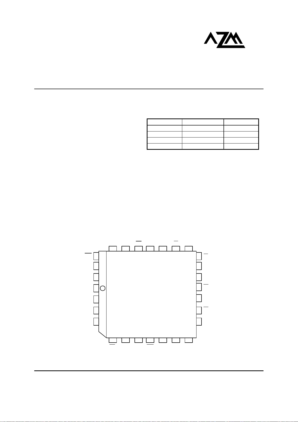
PACKAGE AVAILABILITY
PACKAGE PART NO. MARKING
PLCC 28 AZ10E131FN AZM10E131
PLCC 28 T&R AZ10E131FNR2 AZM10E131
PLCC 28 AZ100E131FN AZM100E131
PLCC 28 T&R AZ100E131FNR2 AZM100E131
26
27
28
1
2
3
4
V
CCO
V
CC
NC V
CCO
V
EE
25 24 23 22 21 20 19
18
17
16
15
14
13
12
111098765
R3 D2 CE2 R2 Q3 Q3
Q2
Q2
Q1
Q1
Q0
Q0
R1CE1D1R0CE0
D0
S03
C
C
S12
D3
CE3
* All VCC and V
CCO
pins are tied together on the die.
Pinout: 28-Lead
PLCC (top view)
Page 2
AZ10E131
AZ100E131
October 2001 * REV - 2 www.azmicrotek.com
2
Absolute Maximum Ratings are those values beyond which device life may be impaired.
Symbol Characteristic Rating Unit
VCC PECL Power Supply (VEE = 0V) 0 to +8.0 Vdc
VI PECL Input Voltage (V
EE
= 0V) 0 to +6.0 Vdc
VEE ECL Power Supply (VCC = 0V) -8.0 to 0 Vdc
VI ECL Input Voltage (VCC = 0V) -6.0 to 0 Vdc
I
OUT
Output Current --- Continuous
--- Surge
50
100
mA
TA Operating Temperature Range -40 to +85
°C
T
STG
Storage Temperature Range -65 to +150
°C
10K ECL DC Characteristics (VEE = -4.94V to -5.46V, VCC = V
CCO
= GND)
-40°C 0°C 25°C 85°C
Symbol Characteristic
Min Typ Max Min Typ Max Min Typ Max Min Typ Max
Unit
VOH Output HIGH Voltage1 -1080 -890 -1020 -840 -980 -810 -910 -720 mV
VOL Output LOW Voltage1 -1950 -1650 -1950 -1630 -1950 -1630 -1950 -1595 mV
VIH Input HIGH Voltage -1230 -890 -1170 -840 -1130 -810 -1060 -720 mV
VIL Input LOW Voltage -1950 -1500 -1950 -1480 -1950 -1480 -1950 -1445 mV
IIH
Input HIGH Current
C
C
S
R,
CE¯¯
D
350
450
300
150
350
450
300
150
350
450
300
150
350
450
300
150
µA
IIL
Input LOW Current 0.5 0.5 0.5 0.5
µA
IEE Power Supply Current 58 70 58 70 58 70 58 70 mA
1. Each output is terminated through a 50Ω resistor to V
CC
– 2V.
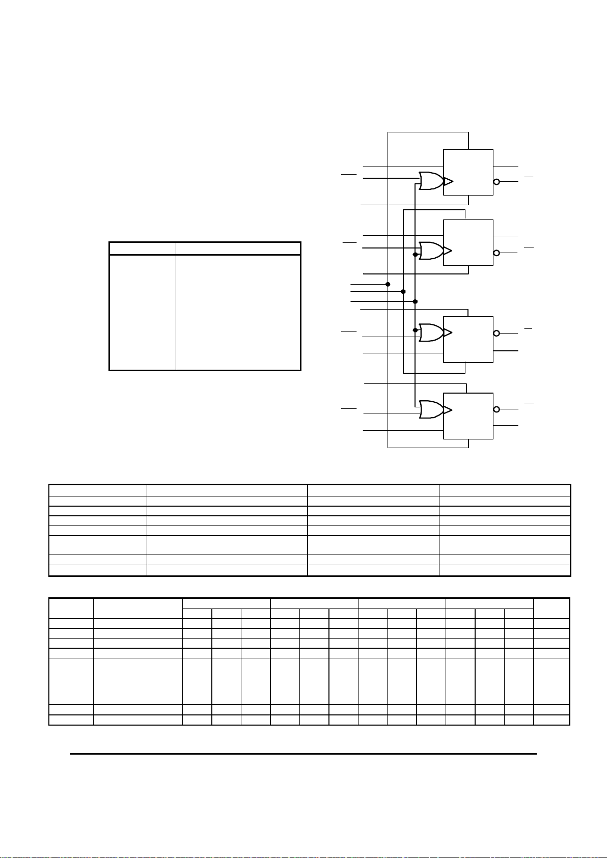
LOGIC SYMBOL
S
D
R
S
D
R
R
D
S
R
D
S
D3
D2
R2
R1
CE1
R0
CE0
D0
Q2
Q0
Q0
Q1
Q1
Q2
Q3
Q3
CE3
R3
CE2
S03
S12
C
C
D1
PIN DESCRIPTION
PIN FUNCTION
D0 – D3 Data inputs
CE0¯¯¯ – CE3¯¯¯ Clock Enables (Individual)
R0 – R3 Resets
CC Common Clock
S03,S12 Sets (paired)
Q0 – Q3 True Outputs
Q0¯¯ – Q3¯¯ Inverting Outputs
V
CC
, V
CCO
Positive Supply
V
EE
Negative Supply
NC No connect
Page 3

AZ10E131
AZ100E131
October 2001 * REV - 2 www.azmicrotek.com
3
10K PECL DC Characteristics (V
EE
= GND, VCC = V
CCO
= +5.0V)
-40°C 0°C 25°C 85°C
Symbol Characteristic
Min T
yp
Max Min T
yp
Max Min T
yp
Max Min T
yp
Max
Unit
VOH Output HIGH Voltage
1,2
3920 4110 3980 4160 4020 4190 4090 4280 mV
VOL Output LOW Voltage
1,2
3050 3350 3050 3370 3050 3370 3050 3405 mV
VIH Input HIGH Voltage1 3770 4110 3830 4160 3870 4190 3940 4280 mV
VIL Input LOW Voltage1 3050 3500 3050 3520 3050 3520 3050 3555 mV
IIH
Input HIGH Current
C
C
S
R,
CE¯¯
D
350
450
300
150
350
450
300
150
350
450
300
150
350
450
300
150
µA
IIL
Input LOW Current 0.5 0.5 0.5 0.5
µA
IEE Power Supply Current 58 70 58 70 58 70 58 70 mA
1. For supply voltages other that 5.0V, use the ECL table values and ADD supply voltage value.
2. Each output is terminated through a 50Ω resistor to V
CC
– 2V.
100K ECL DC Characteristics (V
EE
= -4.2V to -5.46V, VCC = V
CCO
= GND)
-40°C 0°C 25°C 85°C
Symbol Characteristic
Min Typ Max Min Typ Max Min Typ Max Min Typ Max
Unit
VOH Output HIGH Voltage1 -1085 -1005 -880 -1025 -955 -880 -1025 -955 -880 -1025 -955 -880 mV
VOL Output LOW Voltage1 -1830 -1695 -1555 -1810 -1705 -1620 -1810 -1705 -1620 -1810 -1705 -1620 mV
VIH Input HIGH Voltage -1165 -880 -1165 -880 -1165 -880 -1165 -880 mV
VIL Input LOW Voltage -1810 -1475 -1810 -1475 -1810 -1475 -1810 -1475 mV
IIH
Input HIGH Current
C
C
S
R,
CE¯¯
D
350
450
300
150
350
450
300
150
350
450
300
150
350
450
300
150
µA
IIL
Input LOW Current 0.5 0.5 0.5 0.5
µA
IEE Power Supply Current 58 70 58 70 58 70 67 81 mA
1. Each output is terminated through a 50Ω resistor to V
CC
– 2V.
100K PECL DC Characteristics (VEE = GND, VCC = V
CCO
= +5.0V)
-40°C 0°C 25°C 85°C
Symbol Characteristic
Min T
yp
Max Min T
yp
Max Min T
yp
Max Min T
yp
Max
Unit
VOH Output HIGH Voltage
1,2
3915 3995 4120 3975 4045 4120 3975 4045 4120 3975 4045 4120 mV
VOL Output LOW Voltage
1,2
3170 3305 3445 3190 3295 3380 3190 3295 3380 3190 3295 3380 mV
VIH Input HIGH Voltage1 3835 4120 3835 4120 3835 4120 3835 4120 mV
VIL Input LOW Voltage1 3190 3525 3190 3525 3190 3525 3190 3525 mV
IIH
Input HIGH Current
C
C
S
R,
CE¯¯
D
350
450
300
150
350
450
300
150
350
450
300
150
350
450
300
150
µA
IIL
Input LOW Current 0.5 0.5 0.5 0.5
µA
IEE Power Supply Current 58 70 58 70 58 70 67 81 mA
1. For supply voltages other that 5.0V, use the ECL table values and ADD supply voltage value.
2. Each output is terminated through a 50Ω resistor to V
CC
– 2V.
Page 4

AZ10E131
AZ100E131
October 2001 * REV - 2 www.azmicrotek.com
4
AC Characteristics (V
EE
= 10E(-4.94V to -5.46V), 100E(-4.2V to -5.46V); VCC = V
CCO
= GND or VEE = GND,
V
CC
=V
CCO
= 10E(+4.94V to +5.46V), 100E(+4.2V to +5.46V))
-40°C 0°C 25°C 85°C
Symbol Characteristic
Min Typ Max Min Typ Max Min Typ Max Min Typ Max
Unit
F
max
Max. Toggle Frequency 1100 1400 1100 1400 1100 1400 1100 1400 MHz
t
PLH
/ t
PHL
Propagation Delay to
Output
CE¯¯
C
C
R
S
310
275
300
300
600
600
620
550
750
725
775
775
360
325
350
350
500
500
550
550
700
675
725
725
360
325
350
350
500
500
550
550
700
675
725
725
360
325
350
350
500
500
550
550
700
675
725
725
ps
tS Setup Time2 D 200 20 150 20 150 20 150 20 ps
tH Hold Time2 D 225 -20 175 -20 175 -20 175 -20 ps
tRR Reset Recovery Time 450 150 400 150 400 150 400 150 ps
tPW
Minimum Pulse Width
CLK, S, R 400 400 400 400
ps
t
SKEW
Within-Device Skew1 60 60 60 60 ps
tr / tf
Rise/Fall Times
20% - 80%
275 725 300 675 300 675 300 675 ps
1. Within-device skew is defined as identical transitions on similar paths through a device.
2. Setup/hold times guaranteed for both C
C
& CE¯¯ .
Page 5

AZ10E131
AZ100E131
October 2001 * REV - 2 www.azmicrotek.com
5
PACKAGE DIAGRAM
PLCC 28
N
OTES:
1. DATUMS –L-, -M-, AND –N- DETERMINED
WHERE TOP OF LEAD SHOULDER EXITS
PLASTIC BODY AT MOLD PARTING LINE.
2. DIMENSION G1, TRUE POSITION TO BE
MEASURED AT DATUM –T-, SEATING PLANE.
3. DIMENSIONS R AND U DO NOT INCLUDE
MOLD FLASH. ALOWABLE MOLD FLASH IS
0.010mm (0.250in.) PER SIDE.
4. DIMENSIONING AND TOLERANCING PER ANSI
Y14.5M, 1982.
5. CONTROLLING DIMENSION: INCH.
6. THE PACKAGE TOP MAY BE SMALLER THAN
THE PACKGE BOTTOM BY UP TO 0.012mm
(0.300in.). DIMENSIONS R AND U ARE
DETERMINED AT THE OUTERMOST
EXTREMES OF THE PLASTIC BODY
EXCLUSIVE OF MOLD FLASH, THE BAR
BURRS, GATE BURRS AND INTERLEAD FLASH,
BUT INCLUDING ANY MISMATCH BETWEEN
THE TOP AND BOTTOM OF THE PLASTIC
BODY.
7. DIMENSION H DOES NOT INCLUDE DAMBAR
PROTRUSION OR INTRUSION. THE DAMBAR
PROTRUSION(S) SHALL NOT CAUSE THE H
DIMENSION TO BE SMALLER THAN 0.025mm
(0.635in.).
MILLIMETERS INCHES
DIM
MIN MAX MIN MAX
A
12.32 12.57 0.485 0.495
B
12.32 12.57 0.485 0.495
C
4.20 4.57 0.165 0.180
E
2.29 2.79 0.090 0.110
F
0.33 0.48 0.013 0.019
G
1.27 BSC 0.050 BSC
H
0.66 0.81 0.026 0.032
J
0.51 0.020
K
0.64 0.025
R
11.43 11.58 0.450 0.456
U
11.43 11.58 0.450 0.456
V
1.07 1.21 0.042 0.048
W
1.07 1.21 0.042 0.048
X
1.07 1.42 0.042 0.056
T
0.50 0.020
Z
2
O
10O 2
O
10O
G1
10.42 10.92 0.410 0.430
K1
1.02 0.040
Page 6

AZ10E131
AZ100E131
October 2001 * REV - 2 www.azmicrotek.com
6
Arizona Microtek, Inc. reserves the right to change circuitry and specifications at any time without prior notice. Arizona Microtek, Inc.
makes no warranty, representation or guarantee regarding the suitability of its products for any particular purpose, nor does Arizona
Microtek, Inc. assume any liability arising out of the application or use of any product or circuit and specifically disclaims any and all
liability, including without limitation special, consequential or incidental damages. Arizona Microtek, Inc. does not convey any license
rights nor the rights of others. Arizona Microtek, Inc. products are not designed, intended or authorized for use as components in systems
intended to support or sustain life, or for any other application in which the failure of the Arizona Microtek, Inc. product could create a
situation where personal injury or death may occur. Should Buyer purchase or use Arizona Microtek, Inc. products for any such
unintended or unauthorized application, Buyer shall indemnify and hold Arizona Microtek, Inc. and its officers, employees, subsidiaries,
affiliates, and distributors harmless against all claims, costs, damages, and expenses, and reasonable attorney fees arising out of, directly
or indirectly, any claim of personal injury or death associated with such unintended or unauthorized use, even if such claim alleges tha
t
Arizona Microtek, Inc. was negligent regarding the design or manufacture of the part.
 Loading...