

Page 1
AZ10E116
AZ100E116
ECL/PECL Quint Differential Line Receiver
1630 S. STAPLEY DR., SUITE 125 • MESA, ARIZONA 85204 • USA • (480) 962-5881 • FAX (480) 890-2541
www.azmicrotek.com
ARIZONA MICROTEK, INC.
FEATURES
• 500ps Maximum Propagation Delay
• Dedicated V
CCO
Pin for Each Receiver
• Operating Range of 4.2V to 5.46V
• 75kΩ Internal Input Pulldown Resistors
• Direct Replacement for ON Semiconductor
MC10E116 & MC100E116
DESCRIPTION
The AZ10/100E116 is a quint differential line receiver with emitter-follower outputs. The E116 provides a VBB
output for single-ended use or a DC bias reference for AC coupling to the device. For single-ended input
applications, the V
BB
reference should be connected to one side of the Dn/D¯n differential input pair. The input
signal is then fed to the other Dn/D¯ n input. The V
BB
pin should be used only as a bias for the E116 as its sink/source
capability is limited. When used, the V
BB
pin should be bypassed to ground via a 0.01µF capacitor.
The receiver design features clamp circuitry to cause a defined state if both the inverting and non-inverting
inputs are left open; in this case the Q output goes LOW, while the Q¯ output goes HIGH. This feature makes the
device ideal for twisted pair applications.
If both inverting and non-inverting inputs are at an equal potential of > V
CC
-2.5V, the receiver does not go
to a defined state. This condition may produce output voltage levels between HIGH and LOW.
NOTE: Specifications in ECL/PECL tables are valid when thermal equilibrium is established.
PACKAGE AVAILABILITY
PACKAGE PART NO. MARKING
PLCC 28 AZ10E116FN AZM10E116
PLCC 28 T&R AZ10E116FNR2 AZM10E116
PLCC 28 AZ100E116FN AZM100E116
PLCC 28 T&R AZ100E116FNR2 AZM100E116
Page 2
AZ10E116
AZ100E116
October 2001 * REV - 2 www.azmicrotek.com
2
Absolute Maximum Ratings are those values beyond which device life may be impaired.
Symbol Characteristic Rating Unit
VCC PECL Power Supply (VEE = 0V) 0 to +8.0 Vdc
VI PECL Input Voltage (V
EE
= 0V) 0 to +6.0 Vdc
VEE ECL Power Supply (VCC = 0V) -8.0 to 0 Vdc
VI ECL Input Voltage (VCC = 0V) -6.0 to 0 Vdc
I
OUT
Output Current --- Continuous
--- Surge
50
100
mA
TA Operating Temperature Range -40 to +85
°C
T
STG
Storage Temperature Range -65 to +150
°C
10K ECL DC Characteristics (VEE = -4.94V to -5.46V, VCC = V
CCO
= GND)
-40°C 0°C 25°C 85°C
Symbol Characteristic
Min Typ Max Min Typ Max Min Typ Max Min Typ Max
Unit
VOH Output HIGH Voltage1 -1080 -890 -1020 -840 -980 -810 -910 -720 mV
VOL Output LOW Voltage1 -1950 -1650 -1950 -1630 -1950 -1630 -1950 -1595 mV
VIH Input HIGH Voltage -1230 -890 -1170 -840 -1130 -810 -1060 -720 mV
VIL Input LOW Voltage -1950 -1500 -1950 -1480 -1950 -1480 -1950 -1445 mV
VBB Reference Voltage -1430 -1300 -1380 -1270 -1350 -1250 -1310 -1190 mV
IIH
Input HIGH Current 150 150 150 150
µA
IIL
Input LOW Current 0.5 0.5 0.5 0.5
µA
IEE Power Supply Current 29 35 29 35 29 35 29 35 mA
1. Each output is terminated through a 50Ω resistor to V
CC
– 2V.
LOGIC SYMBOL
D0
D0
D1
D1
D2
D2
D3
D3
D4
D4
Q0
Q0
Q1
Q1
Q2
Q2
Q3
Q3
Q4
Q4
V
BB
26
27
28
1
2
3
4
V
CCO
V
CCO
V
EE
V
BB
V
CC
V
CCO
V
CCO
V
CCO
25
24 23 22
21
20
19
18
17
16
15
14
13
12
111098765
D3 D4 D4 Q4 Q4
Q3
Q3
Q2
Q2
Q1
Q1Q0Q0D1D1
D0
D0
D2
D2
D3
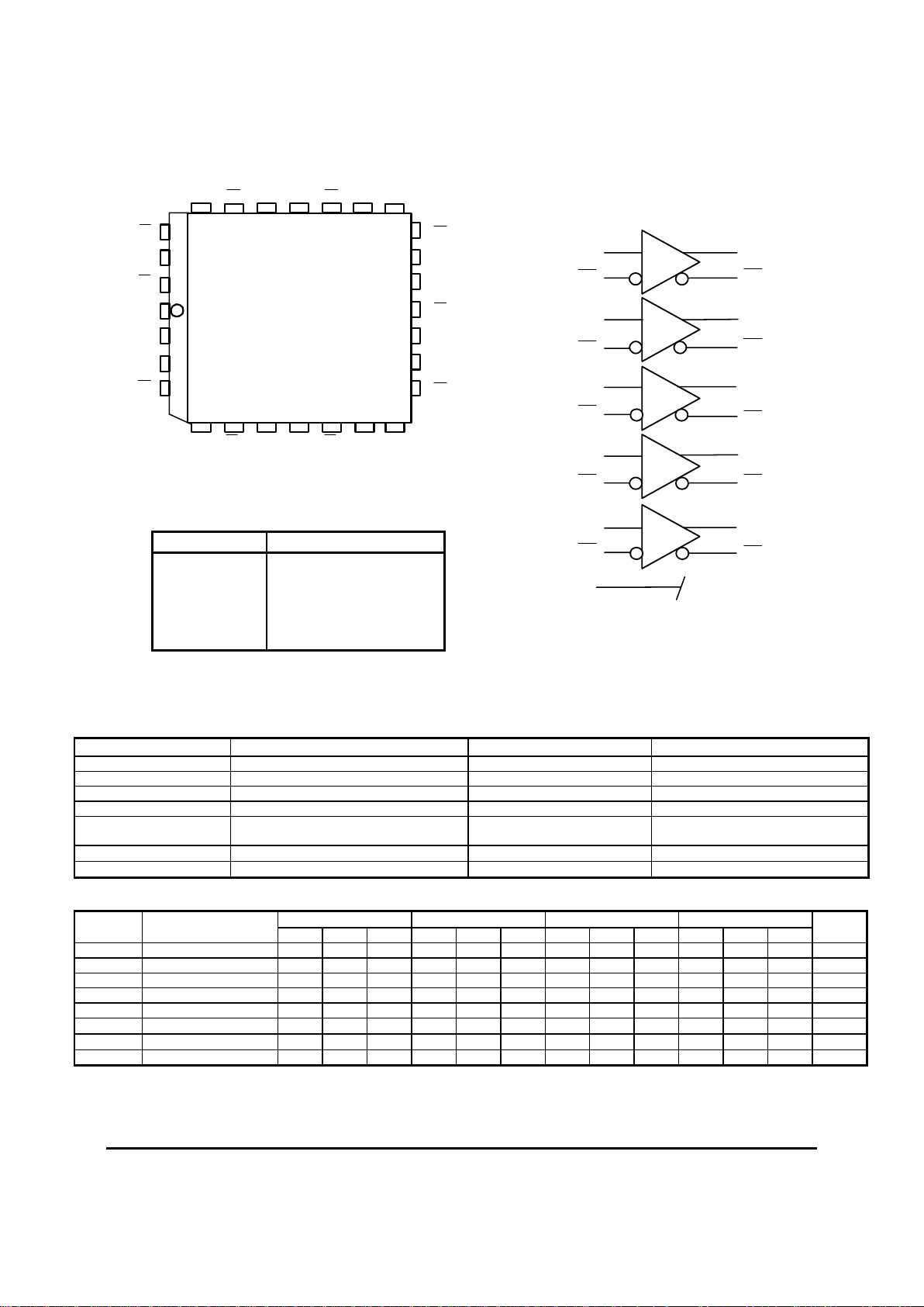
PIN DESCRIPTION
PIN FUNCTION
D0, D0¯¯ -D4, D4¯¯ Differential Input Pairs
Q0, Q0¯¯ -Q4, Q4¯¯ Differential Output Pairs
VBB Reference Voltage Output
V
CC
, V
CCO
Positive Supply
V
EE
Negative Supply
Pinout: 28-lead
PLCC (top view)
Page 3

AZ10E116
AZ100E116
October 2001 * REV - 2 www.azmicrotek.com
3
10K PECL DC Characteristics (V
EE
= GND, VCC = V
CCO
= +5.0V)
-40°C 0°C 25°C 85°C
Symbol Characteristic
Min T
yp
Max Min T
yp
Max Min T
yp
Max Min T
yp
Max
Unit
VOH Output HIGH Voltage
1,2
3920 4110 3980 4160 4020 4190 4090 4280 mV
VOL Output LOW Voltage
1,2
3050 3350 3050 3370 3050 3370 3050 3405 mV
VIH Input HIGH Voltage1 3770 4110 3830 4160 3870 4190 3940 4280 mV
VIL Input LOW Voltage1 3050 3500 3050 3520 3050 3520 3050 3555 mV
VBB Reference Voltage1 3570 3700 3620 3730 3650 3750 3690 3810 mV
IIH Input HIGH Current 150 150 150 150
µA
IIL
Input LOW Current 0.5 0.5 0.5 0.5
µA
IEE Power Supply Current 29 35 29 35 29 35 29 35 mA
1. For supply voltages other that 5.0V, use the ECL table values and ADD supply voltage value.
2. Each output is terminated through a 50Ω resistor to V
CC
– 2V.
100K ECL DC Characteristics (V
EE
= -4.2V to -5.46V, VCC = V
CCO
= GND)
-40°C 0°C 25°C 85°C
Symbol Characteristic
Min Typ Max Min Typ Max Min Typ Max Min Typ Max
Unit
VOH Output HIGH Voltage1 -1085 -1005 -880 -1025 -955 -880 -1025 -955 -880 -1025 -955 -880 mV
VOL Output LOW Voltage1 -1830 -1695 -1555 -1810 -1705 -1620 -1810 -1705 -1620 -1810 -1705 -1620 mV
VIH Input HIGH Voltage -1165 -880 -1165 -880 -1165 -880 -1165 -880 mV
VIL Input LOW Voltage -1810 -1475 -1810 -1475 -1810 -1475 -1810 -1475 mV
VBB Reference Voltage -1380 -1260 -1380 -1260 -1380 -1260 -1380 -1260 mV
IIH
Input HIGH Current 150 150 150 150
µA
IIL
Input LOW Current 0.5 0.5 0.5 0.5
µA
IEE Power Supply Current 29 35 29 35 29 35 29 40 mA
1. Each output is terminated through a 50Ω resistor to V
CC
– 2V.
100K PECL DC Characteristics (VEE = GND, VCC = V
CCO
= +5.0V)
-40°C 0°C 25°C 85°C
Symbol Characteristic
Min T
yp
Max Min T
yp
Max Min T
yp
Max Min T
yp
Max
Unit
VOH Output HIGH Voltage
1,2
3915 3995 4120 3975 4045 4120 3975 4045 4120 3975 4045 4120 mV
VOL Output LOW Voltage
1,2
3170 3305 3445 3190 3295 3380 3190 3295 3380 3190 3295 3380 mV
VIH Input HIGH Voltage1 3835 4120 3835 4120 3835 4120 3835 4120 mV
VIL Input LOW Voltage1 3190 3525 3190 3525 3190 3525 3190 3525 mV
VBB Reference Voltage1 3620 3740 3620 3740 3620 3740 3620 3740 mV
IIH Input HIGH Current 150 150 150 150
µA
IIL
Input LOW Current 0.5 0.5 0.5 0.5
µA
IEE Power Supply Current 29 35 29 35 29 35 29 40 mA
1. For supply voltages other that 5.0V, use the ECL table values and ADD supply voltage value.
2. Each output is terminated through a 50Ω resistor to V
CC
– 2V.
AC Characteristics (VEE =10E(-4.94V to -5.46V), 100E(-4.2V to -5.46V); VCC =V
CCO
=GND or VEE=GND,
V
CC=VCCO
=10E(+4.94V to +5.46V),100E(+4.2V to +5.46V) )
-40°C 0°C 25°C 85°C
Unit
Condition
Symbol Characteristic
Min Typ Max Min Typ Max Min Typ Max Min Typ Max
t
PLH
/t
PHL
Propagation Delay to
Output
D (Differential)
D (Single-Ended)
150
150
300
300
500
550
200
150
300
300
450
500
200
150
300
300
450
500
200
150
300
300
450
500
ps
T
SKEW
Within-Device Skew1 50 50 50 50 ps
T
SKEW
Duty Cycle Skew
2
t
PLH
- t
PHL
±10
±10
±10
±10
ps
Vpp(AC) Minimum Input
Swing
3
150 150 150 150 mV
V
CMR
Common Mode
Range
4
VCC
- 2.0
VCC
- 0.6
VCC
- 2.0
VCC
- 0.6
VCC
- 2.0
VCC
- 0.6
VCC
- 2.0
VCC
- 0.6
V
tr/tf Rise/Fall Time 250 625 275 575 275 575 275 575 ps 20-80%
1. Within-device skew is defined as identical transitions on similar paths through a device.
2. Duty cycle skew is defined only for differential operation. The skews are measured from the crossover point of the inputs to the crossover point
of the outputs.
3. V
PP
is the minimum peak-to-peak differential input swing for which AC parameters are guaranteed.
4. The V
CMR
range is referenced to the most positive side of the differential input signal. Normal operation is obtained if the HIGH level falls within
the specified range and the peak-to-peak voltage lies between V
PP
(min) and 1V.
Page 4

AZ10E116
AZ100E116
October 2001 * REV - 2 www.azmicrotek.com
4
PACKAGE DIAGRAM
PLCC 28
MILLIMETERS INCHES
DIM
MIN MAX MIN MAX
A
12.32 12.57 0.485 0.495
B
12.32 12.57 0.485 0.495
C
4.20 4.57 0.165 0.180
E
2.29 2.79 0.090 0.110
F
0.33 0.48 0.013 0.019
G
1.27 BSC 0.050 BSC
H
0.66 0.81 0.026 0.032
J
0.51 0.020
K
0.64 0.025
R
11.43 11.58 0.450 0.456
U
11.43 11.58 0.450 0.456
V
1.07 1.21 0.042 0.048
W
1.07 1.21 0.042 0.048
X
1.07 1.42 0.042 0.056
T
0.50 0.020
Z
2
O
10O 2
O
10O
G1
10.42 10.92 0.410 0.430
K1
1.02 0.040
N
OTES:
1. DATUMS –L-, -M-, AND –N- DETERMINED
WHERE TOP OF LEAD SHOULDER EXITS
PLASTIC BODY AT MOLD PARTING LINE.
2. DIMENSION G1, TRUE POSITION TO BE
MEASURED AT DATUM –T-, SEATING PLANE.
3. DIMENSIONS R AND U DO NOT INCLUDE
MOLD FLASH. ALOWABLE MOLD FLASH IS
0.010mm (0.250in.) PER SIDE.
4. DIMENSIONING AND TOLERANCING PER ANSI
Y14.5M, 1982.
5. CONTROLLING DIMENSION: INCH.
6. THE PACKAGE TOP MAY BE SMALLER THAN
THE PACKGE BOTTOM BY UP TO 0.012mm
(0.300in.). DIMENSIONS R AND U ARE
DETERMINED AT THE OUTERMOST
EXTREMES OF THE PLASTIC BODY
EXCLUSIVE OF MOLD FLASH, THE BAR
BURRS, GATE BURRS AND INTERLEAD FLASH,
BUT INCLUDING ANY MISMATCH BETWEEN
THE TOP AND BOTTOM OF THE PLASTIC
BODY.
7. DIMENSION H DOES NOT INCLUDE DAMBAR
PROTRUSION OR INTRUSION. THE DAMBAR
PROTRUSION(S) SHALL NOT CAUSE THE H
DIMENSION TO BE SMALLER THAN 0.025mm
(0.635in.).
Page 5

AZ10E116
AZ100E116
October 2001 * REV - 2 www.azmicrotek.com
5
Arizona Microtek, Inc. reserves the right to change circuitry and specifications at any time without prior notice. Arizona Microtek, Inc.
makes no warranty, representation or guarantee regarding the suitability of its products for any particular purpose, nor does Arizona
Microtek, Inc. assume any liability arising out of the application or use of any product or circuit and specifically disclaims any and all
liability, including without limitation special, consequential or incidental damages. Arizona Microtek, Inc. does not convey any license
rights nor the rights of others. Arizona Microtek, Inc. products are not designed, intended or authorized for use as components in systems
intended to support or sustain life, or for any other application in which the failure of the Arizona Microtek, Inc. product could create a
situation where personal injury or death may occur. Should Buyer purchase or use Arizona Microtek, Inc. products for any such
unintended or unauthorized application, Buyer shall indemnify and hold Arizona Microtek, Inc. and its officers, employees, subsidiaries,
affiliates, and distributors harmless against all claims, costs, damages, and expenses, and reasonable attorney fees arising out of, directly
or indirectly, any claim of personal injury or death associated with such unintended or unauthorized use, even if such claim alleges tha
t
Arizona Microtek, Inc. was negligent regarding the design or manufacture of the part.
 Loading...