

Datasheet AZ100LVEL58TR2, AZ100LVEL58TR1, AZ100LVEL58T, AZ100LVEL58DR2, AZ100LVEL58DR1 Datasheet (AZMIC)
...Page 1
AZ100LVEL58
ECL/PECL 2:1 Multiplexer
1630 S. STAPLEY DR., SUITE 125 • MESA, ARIZONA 85204 • USA • (480) 962-5881 • FAX (480) 890-2541
www.azmicrotek.com
ARIZONA MICROTEK, INC.
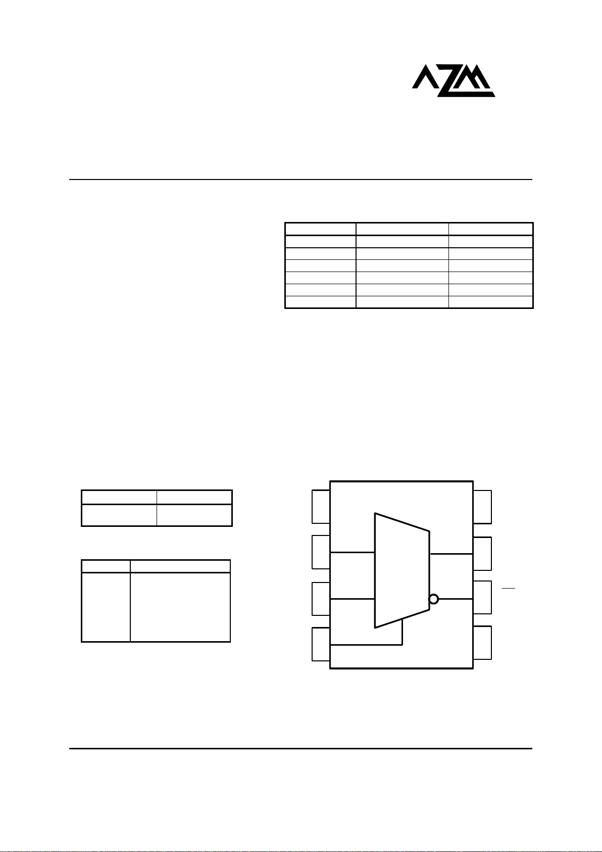
FUNCTION TABLE
SEL Q
H Da
L Db
FEATURES
• 440ps Propagation Delay
• Operating Range of 3.0V to 5.5V
• Internal Input Pulldown Resistors
• Q Output will Default LOW with Inputs Open
or at V
EE
• Transistor Count = 58 Devices
• Direct Replacement for ON Semiconductor
MC100LVEL58
DESCRIPTION
The AZ100LVEL58 is a 2:1 multiplexer. The device is pin and functionally equivalent to the EL58. With AC
performance similar to the EL58 device, the LVEL58 is ideal for the low voltage applications that require the
ultimate in AC performance. If desired, the select input can be directly driven from a CMOS output.
NOTE: Specifications in the ECL/PECL tables are valid when thermal equilibrium is established.
PACKAGE AVAILABILITY
PACKAGE PART NO. MARKING
SOIC 8 AZ100LVEL58D AZM100LVEL58
SOIC 8 T&R AZ100LVEL58DR1 AZM100LVEL58
SOIC 8 T&R AZ100LVEL58DR2 AZM100LVEL58
TSSOP 8 AZ100LVEL58T AZTLV58
TSSOP 8 T&R AZ100LVEL58TR1 AZTLV58
TSSOP 8 T&R AZ100LVEL58TR2 AZTLV58
LOGIC DIAGRAM AND PINOUT ASSIGNMENT
8
5
6
7
4
3
2
1
V
CC
Da
V
EE
NC
Q
Q
SEL
MUX
Db
PIN DESCRIPTION
PIN FUNCTION
Da, Db Data Inputs
Q, Q¯ Differential Outputs
SEL Select Input
VCC Positive Supply
VEE Negative Supply
NC No Connect
Page 2
AZ100LVEL58
October 2001 * REV-0 www.azmicrotek.com
2
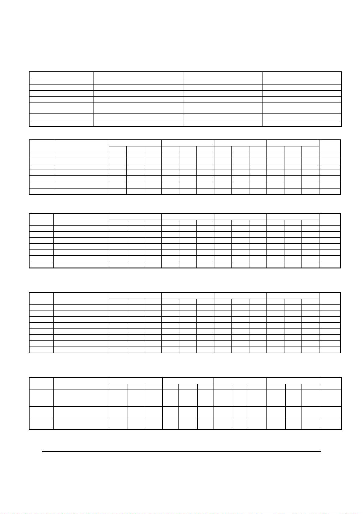
Absolute Maximum Ratings are those values beyond which device life may be impaired.
Symbol Characteristic Rating Unit
VCC PECL Power Supply (VEE = 0V) 0 to +8.0 Vdc
VI PECL Input Voltage (V
EE
= 0V) 0 to +6.0 Vdc
VEE ECL Power Supply (VCC = 0V) -8.0 to 0 Vdc
VI ECL Input Voltage (VCC = 0V) -6.0 to 0 Vdc
I
OUT
Output Current --- Continuous
--- Surge
50
100
mA
TA Operating Temperature Range -40 to +85
°C
T
STG
Storage Temperature Range -65 to +150
°C
100K ECL DC Characteristics (VEE = -3.3V, VCC = GND)
-40°C 0°C 25°C 85°C
Symbol Characteristic
Min Typ Max Min Typ Max Min Typ Max Min Typ Max
Unit
VOH Output HIGH Voltage1 -1085 -1005 -880 -1025 -955 -880 -1025 -955 -880 -1025 -955 -880 mV
VOL Output LOW Voltage1 -1830 -1695 -1555 -1810 -1705 -1620 -1810 -1705 -1620 -1810 -1705 -1620 mV
VIH Input HIGH Voltage -1165 -880 -1165 -880 -1165 -880 -1165 -880 mV
VIL Input LOW Voltage -1810 -1475 -1810 -1475 -1810 -1475 -1810 -1475 mV
IIH
Input HIGH Current 150 150 150 150
µA
I
IL
Input LOW Current -150 -150 -150 -150
µA
IEE Power Supply Current 21 28 21 28 21 28 23 30 mA
1. Each output is terminated through a 50Ω resistor to V
CC
– 2V.
100K LVPECL DC Characteristics (VEE = GND, VCC = +3.3V)
-40°C 0°C 25°C 85°C
Symbol Characteristic
Min T
yp
Max Min T
yp
Max Min T
yp
Max Min T
yp
Max
Unit
VOH Output HIGH Voltage
1,2
2215 2295 2420 2275 2345 2420 2275 2345 2420 2275 2345 2420 mV
VOL Output LOW Voltage
1,2
1470 1605 1745 1490 1595 1680 1490 1595 1680 1490 1595 1680 mV
VIH Input HIGH Voltage1 2135 2420 2135 2420 2135 2420 2135 2420 mV
VIL Input LOW Voltage1 1490 1825 1490 1825 1490 1825 1490 1825 mV
IIH Input HIGH Current 150 150 150 150
µA
I
IL
Input LOW Current -150 -150 -150 -150
µA
IEE Power Supply Current 21 28 21 28 21 28 23 30 mA
1. These values are for VCC = 3.3V. For supply voltages other that 3.3V, use the ECL table values and ADD supply voltage value.
2. Each output is terminated through a 50Ω resistor to V
CC
– 2V.
100K PECL DC Characteristics (VEE = GND, VCC = +5.0V)
-40°C 0°C 25°C 85°C
Symbol Characteristic
Min T
yp
Max Min T
yp
Max Min T
yp
Max Min T
yp
Max
Unit
VOH Output HIGH Voltage
1,2
3915 3995 4120 3975 4045 4120 3975 4045 4120 3975 4045 4120 mV
VOL Output LOW Voltage
1,2
3170 3305 3445 3190 3295 3380 3190 3295 3380 3190 3295 3380 mV
VIH Input HIGH Voltage1 3835 4120 3835 4120 3835 4120 3835 4120 mV
VIL Input LOW Voltage1 3190 3525 3190 3525 3190 3525 3190 3525 mV
VBB Reference Voltage1 3620 3740 3620 3740 3620 3740 3620 3740 mV
IIH
Input HIGH Current 150 150 150
µA
IIL Input LOW Current -150 -150 -150 -150 150
µA
IEE Power Supply Current 27 33 27 33 27 33 31 37 mA
1. For supply voltages other that 5.0V, use the ECL table values and ADD supply voltage value.
2. Each output is terminated through a 50Ω resistor to V
CC
– 2V.
AC Characteristics (VEE = -3.0V to -5.5V, VCC = GND or VEE GND, VCC = +3.0V to +5.5V)
-40°C 0°C 25°C 85°C
Symbol Characteristic
Min Typ Max Min Typ Max Min Typ Max Min Typ Max
Unit
t
PLH
/ t
PHL
Propagation Delay to
Output D to Q
SEL to Q
340
540
435
455
560
570
350
360
440
460
570
580
370
380
450
470
590
600
ps
f
max
Maximum Toggle
Frequency
1.5 GHz
tr / tf
Rise/Fall Time
20 – 80%
100 260 100 260 100 260 100 260 ps
Page 3

AZ100LVEL58
October 2001 * REV-0 www.azmicrotek.com
3
MILLIMETERS INCHES
DIM
MIN MAX MIN MAX
A
1.75 0.069
A1
0.10 0.25 0.004 0.010
A2
1.25 1.45 0.049 0.057
A3
0.25 0.01
bp
0.36 0.49 0.014 0.019
c
0.19 0.25 0.0075 0.0100
D
4.8 5.0 0.19 0.20
E
3.8 4.0 0.15 0.16
e
1.27 0.050
HE
5.80 6.20 0.228 0.244
L
1.05 0.041
Lp
0.40 1.00 0.016 0.039
Q
0.60 0.70 0.024 0.028
v
0.25 0.01
w
0.25 0.01
y
0.10 0.004
Z
0.30 0.70 0.012 0.028
θ
0
O
8
O
0
O
8
O
N
OTES:
1. DIMENSIONS D AND E DO NOT
INCLUDE MOLD PROTRUSION.
2. MAXIMUM MOLD PROTRUSION
FOR D IS 0.15mm.
3. MAXIMUM MOLD PROTRUSION
FOR E IS 0.25mm.
PACKAGE DIAGRAM
SOIC 8
Page 4

AZ100LVEL58
October 2001 * REV-0 www.azmicrotek.com
4
PACKAGE DIAGRAM
TSSOP 8
MILLIMETERS
DIM
MIN MAX
A
1.10
A1
0.05 0.15
A2
0.80 0.95
A3
0.25
bp
0.25 0.45
c
0.15 0.28
D
2.90 3.10
E
2.90 3.10
e
0.65
HE
4.70 5.10
L
0.94
Lp
0.40 0.70
v
0.10
w
0.10
y
0.10
Z
0.35 0.70
θ
0
O
6
O
N
OTES:
1. DIMENSIONS D AND E DO NOT
INCLUDE MOLD PROTRUSION.
2. MAXIMUM MOLD PROTRUSION
FOR D IS 0.15mm.
3. MAXIMUM MOLD PROTRUSION
FOR E IS 0.25mm.
Page 5

AZ100LVEL58
October 2001 * REV-0 www.azmicrotek.com
5
Arizona Microtek, Inc. reserves the right to change circuitry and specifications at any time without prior notice. Arizona Microtek, Inc.
makes no warranty, representation or guarantee regarding the suitability of its products for any particular purpose, nor does Arizona
Microtek, Inc. assume any liability arising out of the application or use of any product or circuit and specifically disclaims any and all
liability, including without limitation special, consequential or incidental damages. Arizona Microtek, Inc. does not convey any license
rights nor the rights of others. Arizona Microtek, Inc. products are not designed, intended or authorized for use as components in systems
intended to support or sustain life, or for any other application in which the failure of the Arizona Microtek, Inc. product could create a
situation where personal injury or death may occur. Should Buyer purchase or use Arizona Microtek, Inc. products for any such
unintended or unauthorized application, Buyer shall indemnify and hold Arizona Microtek, Inc. and its officers, employees, subsidiaries,
affiliates, and distributors harmless against all claims, costs, damages, and expenses, and reasonable attorney fees arising out of, directly
or indirectly, any claim of personal injury or death associated with such unintended or unauthorized use, even if such claim alleges tha
t
Arizona Microtek, Inc. was negligent regarding the design or manufacture of the part.
 Loading...