

Datasheet AZ10EL16VOX, AZ10EL16VOTR2, AZ10EL16VOTR1, AZ10EL16VOT, AZ10EL16VOLR2 Datasheet (AZMIC)
...Page 1
AZ10EL16VO
AZ100EL16VO
ECL/PECL Oscillator Gain Stage and Buffer with Enable
1630 S. STAPLEY DR., SUITE 125 • MESA, ARIZONA 85204 • USA • (480) 962-5881 • FAX (480) 890-2541
www.azmicrotek.com
ARIZONA MICROTEK, INC.
FEATURES
• 250ps Propagation Delay on Q¯ Output
• High Voltage Gain vs. Standard EL16
• For Oscillator Applications
• Operating Range of 3.0V to 5.5V
• Available in 2x2 or 3x3mm MLP Package
• 75kΩ Enable Pull-Down Resistor
DESCRIPTION
The AZ10/100EL16VO is a specialized oscillator gain stage with a high gain output buffer including an enable.
The Q
HG
/Q¯HG outputs have a voltage gain several times greater than the Q/Q¯ outputs.
The EL16VO provides an enable input (EN¯¯ ) that allows continuous oscillator operation. When EN¯¯ is LOW or
floating (NC), input data is passed to both sets of outputs. When EN¯¯ is HIGH, the Q
HG
/Q¯HG outputs will be forced
LOW/HIGH respectively, while input data will continue to be passed to the Q/Q¯ outputs. The EN¯¯ input can be
driven with an ECL/PECL signal or a full supply swing CMOS type logic signal.
The EL16VO also provides a V
BB
output for a crystal bias node. The VBB pin can support 1.5mA sink/source
current. When used, the V
BB
pin should be bypassed to ground via a 0.01µF capacitor.
Any used output must have an external pull down resistor. For 3.3V operation, a 180Ω resistor to V
EE
is
recommended if an AC coupled load is present. At 5.0V, a 330Ω resistor is recommended for the AC load case.
Alternately, a 50Ω load terminated to V
CC
– 2V may be driven directly. Unused outputs may be left floating (NC).
NOTE: Specifications in ECL/PECL tables are valid when thermal equilibrium is established.
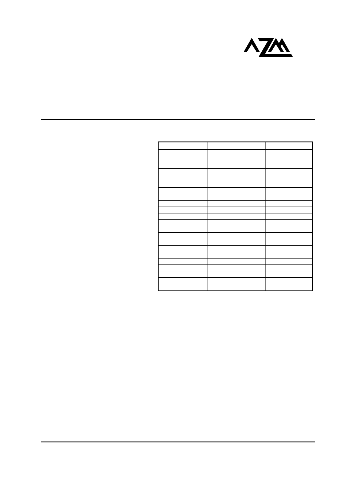
PACKAGE AVAILABILITY
PACKAGE PART NO. MARKING
MLP 8 (2x2x0.75) AZ100EL16VONB TNB
MLP 8 (2x2x0.75)
T&R
AZ100EL16VONBR1 TNB
MLP 8 (2x2x0.75)
T&R
AZ100EL16VONBR2 TNB
MLP 16 AZ10/100EL16VOL AZM16J
MLP 16 T&R AZ10/100EL16VOLR1 AZM16J
MLP 16 T&R AZ10/100EL16VOLR2 AZM16J
SOIC 8 AZ10EL16VOD AZM10EL16VO
SOIC 8 T&R AZ10EL16VODR1 AZM10EL16VO
SOIC 8 T&R AZ10EL16VODR2 AZM10EL16VO
SOIC 8 AZ100EL16VOD AZM100EL16VO
SOIC 8 T&R AZ100EL16VODR1 AZM100EL16VO
SOIC 8 T&R AZ100EL16VODR2 AZM100EL16VO
TSSOP 8 AZ10EL16VOT AZT16VO
TSSOP 8 T&R AZ10EL16VOTR1 AZT16VO
TSSOP 8 T&R AZ10EL16VOTR2 AZT16VO
TSSOP 8 AZ100EL16VOT AZH16VO
TSSOP 8 AZ100EL16VOT AZH16VO
TSSOP 8 T&R AZ100EL16VOTR1 AZH16VO
TSSOP 8 T&R AZ100EL16VOTR2 AZH16VO
DIE AZ10/100EL16VOX N/A
Page 2
AZ10EL16VO
AZ100EL16VO
August 2003 * REV - 6 www.azmicrotek.com
2
Q
HG
Q
Q
D
D
EN
V
BB
Q
HG
PIN DESCRIPTION
PIN FUNCTION
D/D¯ Data Inputs
Q/Q¯ Data Outputs
QHG/Q¯HG Data Outputs w/High Gain
VBB Reference Voltage Output
EN¯¯ Enable Input
V
CC
Positive Supply
V
EE
Negative Supply
Absolute Maximum Ratings are those values beyond which device life may be impaired.
Symbol Characteristic Rating Unit
VCC PECL Power Supply (VEE = 0V) 0 to +8.0 Vdc
VI PECL Input Voltage (V
EE
= 0V) 0 to +6.0 Vdc
VEE ECL Power Supply (VCC = 0V) -8.0 to 0 Vdc
VI ECL Input Voltage (VCC = 0V) -6.0 to 0 Vdc
I
OUT
Output Current — Continuous
— Surge
50
100
mA
TA Operating Temperature Range -40 to +85
°C
T
STG
Storage Temperature Range -65 to +150
°C
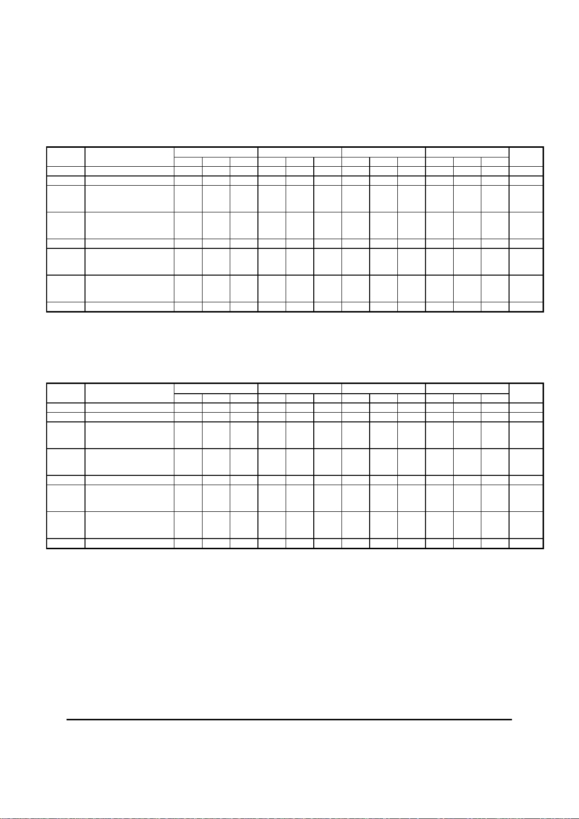
10K ECL DC Characteristics (VEE = -3.0V to -5.5V, VCC = GND)
-40°C 0°C 25°C 85°C
Symbol Characteristic
Min Typ Max Min Typ Max Min Typ Max Min Typ Max
Unit
VOH Output HIGH Voltage1 -1080 -890 -1020 -840 -980 -810 -910 -720 mV
VOL Output LOW Voltage1 -1950 -1650 -1950 -1630 -1950 -1630 -1950 -1595 mV
VIH
Input HIGH Voltage
D/D¯
EN¯¯
-1230
-1230
-890
V
CC
-1170
-1170
-840
VCC
-1130
-1130
-810
VCC
-1060
-1060
-720
VCC
mV
VIL
Input LOW Voltage
D/D¯
EN¯¯
-1950
V
EE
-1500
-1500
-1950
VEE
-1480
-1480
-1950
VEE
-1480
-1480
-1950
VEE
-1445
-1445
mV
VBB Reference Voltage -1430 -1300 -1380 -1270 -1370 -1250 -1310 -1190 mV
IIH
Input HIGH Current
D/D¯
EN¯¯
60
150
60
150
60
150
60
150
µA
IIL
Input LOW Current 0.5 0.5 0.5 0.5
µA
IEE Power Supply Current 40 40 40 40 mA
1. Each output is terminated through a 50Ω resistor to V
CC
– 2V.
TRUTH TABLE
EN¯¯ Q/Q¯ Q
HG
Q¯HG
LOW or NC Data Data Data
HIGH
Data LOW HIGH
NC = No Connect
Page 3
AZ10EL16VO
AZ100EL16VO
August 2003 * REV - 6 www.azmicrotek.com
3
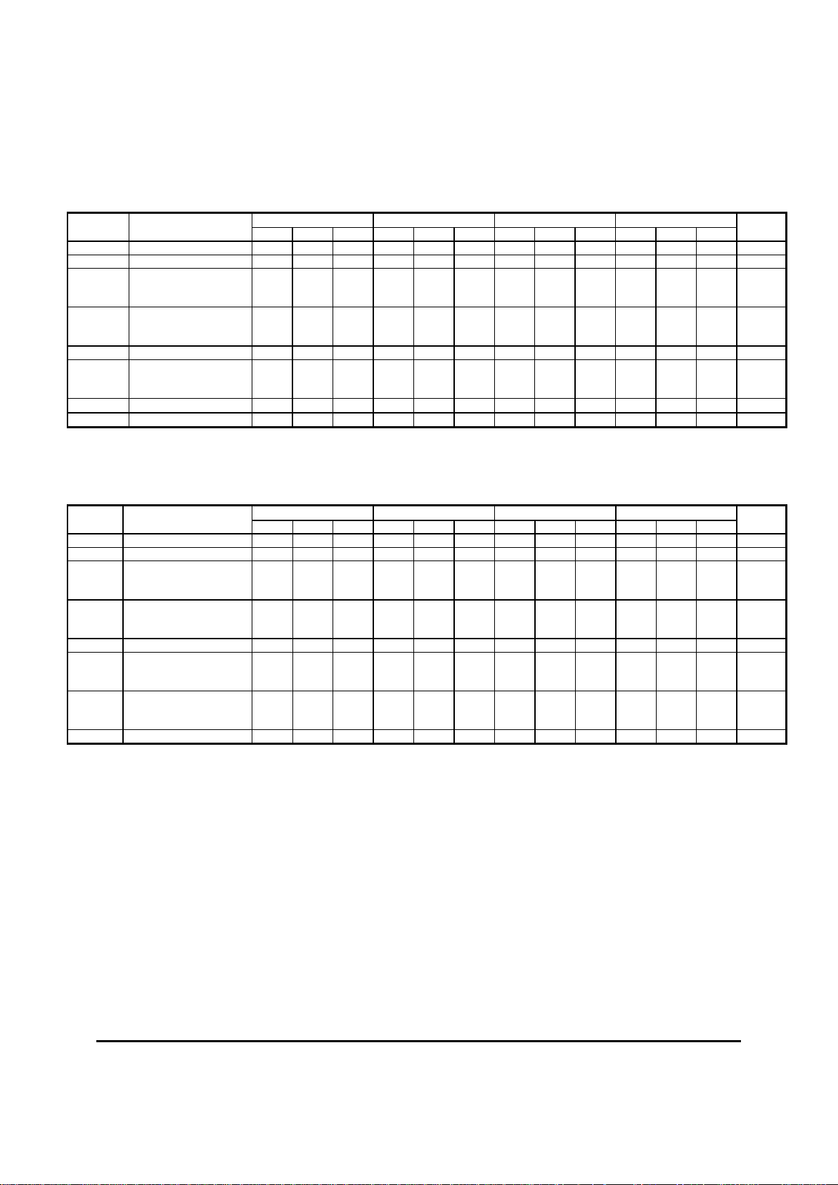
10K LVPECL DC Characteristics (V
EE
= GND, VCC = +3.3V)
-40°C 0°C 25°C 85°C
Symbol Characteristic
Min T
yp
Max Min T
yp
Max Min T
yp
Max Min T
yp
Max
Unit
VOH Output HIGH Voltage
1,2
2220 2410 2280 2460 2320 2490 2390 2580 mV
VOL Output LOW Voltage
1,2
1350 1650 1350 1670 1350 1670 1350 1705 mV
VIH
Input HIGH Voltage
D/D¯1
EN¯¯
2070
2070
1
2410
VCC
2130
21301
2460
VCC
2170
21701
2490
VCC
2240
22401
2580
VCC
mV
VIL
Input LOW Voltage
D/D¯
1
EN¯¯
1350
V
EE
1800
18001
1350
VEE
1820
18201
1350
VEE
1820
18201
1350
VEE
1855
18551
mV
VBB Reference Voltage1 1870 2000 1920 2030 1930 2050 1990 2110 mV
IIH
Input HIGH Current
D/D¯
EN¯¯
60
150
60
150
60
150
60
150
µA
IIL
Input LOW Current
D/D¯
EN¯¯
3
0.5
-300
0.5
-300
0.5
-300
0.5
-300
µA
IEE Power Supply Current 40 40 40 40 mA
1. For supply voltages other that 3.3V, use the ECL table values and ADD supply voltage value.
2. Each output is terminated through a 50Ω resistor to V
CC
– 2V.
3. Specified with EN¯¯ forced to V
EE
.
10K PECL DC Characteristics (V
EE
= GND, VCC = +5.0V)
-40°C 0°C 25°C 85°C
Symbol Characteristic
Min T
yp
Max Min T
yp
Max Min T
yp
Max Min T
yp
Max
Unit
VOH Output HIGH Voltage
1,2
3920 4110 3980 4160 4020 4190 4090 4280 mV
VOL Output LOW Voltage
1,2
3050 3350 3050 3370 3050 3370 3050 3405 mV
VIH
Input HIGH Voltage
D/D¯1
EN¯¯
3770
3770
1
4110
VCC
3830
38301
4160
VCC
3870
38701
4190
VCC
3940
39401
4280
VCC
mV
VIL
Input LOW Voltage
D/D¯1
EN¯¯
3050
V
EE
3500
35001
3050
VEE
3520
35201
3050
VEE
3520
35201
3050
VEE
3555
35551
mV
VBB Reference Voltage1 3570 3700 3620 3730 3630 3750 3690 3810 mV
IIH
Input HIGH Current
D/D¯
EN¯¯
60
150
60
150
60
150
60
150
µA
IIL
Input LOW Current
D/D¯
EN¯¯
3
0.5
-1400
0.5
-1400
0.5
-1400
0.5
-1400
µA
IEE Power Supply Current 40 40 40 40 mA
1. For supply voltages other that 5.0V, use the ECL table values and ADD supply voltage value.
2. Each output is terminated through a 50Ω resistor to V
CC
– 2V.
3. Specified with EN¯¯ forced to V
EE
.
Page 4
AZ10EL16VO
AZ100EL16VO
August 2003 * REV - 6 www.azmicrotek.com
4
100K ECL DC Characteristics (V
EE
= -3.0V to -5.5V, VCC = GND)
-40°C 0°C 25°C 85°C
Symbol Characteristic
Min Typ Max Min Typ Max Min Typ Max Min Typ Max
Unit
VOH Output HIGH Voltage1 -1085 -1005 -880 -1025 -955 -880 -1025 -955 -880 -1025 -955 -880 mV
VOL Output LOW Voltage1 -1900 -1695 -1555 -1900 -1705 -1620 -1900 -1705 -1620 -1900 -1705 -1620 mV
VIH
Input HIGH Voltage
D/D¯
EN¯¯
-1165
-1165
-880
V
CC
-1165
-1165
-880
VCC
-1165
-1165
-880
VCC
-1165
-1165
-880
VCC
mV
VIL
Input LOW Voltage
D/D¯
EN¯¯
-1810
V
EE
-1475
-1475
-1810
VEE
-1475
-1475
-1810
VEE
-1475
-1475
-1810
VEE
-1475
-1475
mV
VBB Reference Voltage -1400 -1260 -1400 -1260 -1400 -1260 -1400 -1260 mV
IIH
Input HIGH Current
D/D¯
EN¯¯
60
150
60
150
60
150
60
150
µA
IIL
Input LOW Current 0.5 0.5 0.5 0.5
µA
IEE Power Supply Current 40 40 40 46 mA
1. Each output is terminated through a 50Ω resistor to V
CC
– 2V.
100K LVPECL DC Characteristics (V
EE
= GND, VCC = +3.3V)
-40°C 0°C 25°C 85°C
Symbol Characteristic
Min T
yp
Max Min T
yp
Max Min T
yp
Max Min T
yp
Max
Unit
VOH Output HIGH Voltage
1,2
2215 2295 2420 2275 2345 2420 2275 2345 2420 2275 2345 2420 mV
VOL Output LOW Voltage
1,2
1400 1605 1745 1400 1595 1680 1400 1595 1680 1400 1595 1680 mV
VIH
Input HIGH Voltage
D/D¯1
EN¯¯
2135
2135
1
2420
VCC
2135
21351
2420
VCC
2135
21351
2420
VCC
2135
21351
2420
VCC
mV
VIL
Input LOW Voltage
D/D¯1
EN¯¯
1490
V
EE
1825
18251
1490
VEE
1825
18251
1490
VEE
1825
18251
1490
VEE
1825
18251
mV
VBB Reference Voltage1 1900 2040 1900 2040 1900 2040 1900 2040 mV
IIH
Input HIGH Current
D/D¯
EN¯¯
60
150
60
150
60
150
60
150
µA
IIL
Input LOW Current
D/D¯
EN¯¯
3
0.5
-300
0.5
-300
0.5
-300
0.5
-300
µA
IEE Power Supply Current 40 40 40 46 mA
1. For supply voltages other that 3.3V, use the ECL table values and ADD supply voltage value.
2. Each output is terminated through a 50Ω resistor to V
CC
– 2V.
3. Specified with EN¯¯ forced to V
EE
.
Page 5

AZ10EL16VO
AZ100EL16VO
August 2003 * REV - 6 www.azmicrotek.com
5
100K PECL DC Characteristics (V
EE
= GND, VCC = +5.0V)
-40°C 0°C 25°C 85°C
Symbol Characteristic
Min T
yp
Max Min T
yp
Max Min T
yp
Max Min T
yp
Max
Unit
VOH Output HIGH Voltage
1,2
3915 3995 4120 3975 4045 4120 3975 4045 4120 3975 4045 4120 mV
VOL Output LOW Voltage
1,2
3100 3305 3445 3100 3295 3380 3100 3295 3380 3100 3295 3380 mV
VIH
Input HIGH Voltage
D/D¯1
EN¯¯
3835
3835
1
4120
VCC
3835
38351
4120
VCC
3835
38351
4120
VCC
3835
38351
4120
VCC
mV
VIL
Input LOW Voltage
D/D¯1
EN¯¯
3190
V
EE
3525
35251
3190
VEE
3525
35251
3190
VEE
3525
35251
3190
VEE
3525
35251
mV
VBB Reference Voltage1 3600 3740 3600 3740 3600 3740 3600 3740 mV
IIH
Input HIGH Current
D/D¯
EN¯¯
60
150
60
150
60
150
60
150
µA
IIL
Input LOW Current
D/D¯
EN¯¯
3
0.5
-1400
0.5
-1400
0.5
-1400
0.5
-1400
µA
IEE Power Supply Current 40 40 40 46 mA
1. For supply voltages other that 5.0V, use the ECL table values and ADD supply voltage value.
2. Each output is terminated through a 50Ω resistor to V
CC
– 2V.
3. Specified with EN¯¯ forced to V
EE
.
AC Characteristics (V
EE
= -3.0V to -5.5V; VCC = GND or VEE = GND, VCC = +3.0V to +5.5V)
-40°C 0°C 25°C 85°C
Symbol Characteristic
Min Typ Max Min Typ Max Min Typ Max Min Typ Max
Unit
t
PLH/tPHL
Propagation Delay
D to Q/Q¯ Outputs (SE)
D to Q
HG
/Q¯
HG
Outputs (SE)
400
700
400
700
400
700
430
780
ps
t
SKEW
Duty Cycle Skew1 (SE) 5 5 20 5 20 5 20 ps
V
PP
(AC) Minimum Input Swing2 150 150 150 150 mV
tr/tf
Output Rise/Fall Times
(20% – 80%)
100 350 100 350 100 350 100 350 ps
1. Duty cycle skew is the difference between a t
PLH
and t
PHL
propagation delay through a device.
2. V
PP
is the minimum peak-to-peak differential input swing for which AC parameters are guaranteed. The device has a voltage gain of ≈20 to Q/Q¯
outputs and a voltage gain of ≈100 to Q
HG
/Q¯HG outputs.
Page 6

AZ10EL16VO
AZ100EL16VO
August 2003 * REV - 6 www.azmicrotek.com
6
TIMING DIAGRAM
D
Q
EN
Q
HG
4
3
2
1
D
8
5
6
7
Q
EN
D / V
BB
V
CC
Q
HG
Q
HG
V
EE
TSSOP 8
SOIC 8
MLP 16 Package and DIE:
10K/100K Selection
Connect pin/pad 10K to V
EE
to
select 10K operation. Float (NC)
pin/pad 10K to select 100K
operation. V
EE
connection must be
less than 1Ω.
Pin 6 of the MLP 16 package may
be connected to pin 7 (V
EE
) with no
effect on the circuit.
D
Q
EN
V
EE
Q
HG
Q
HG
V
CC
4
3
2
1
58
7
6
10
9
12
11
V
BB
Q
D
NC
13
14
15
16
NC
NC
NC
NC
10K
MLP 16,
3x3 mm
TOP VIEW
D
4
3
2
1
6
5
8
7
MLP 8, 2x2mm
Q
HG
Q
HG
EN
Q
V
BB
V
EE
V
CC
TOP VIEW
Page 7

AZ10EL16VO
AZ100EL16VO
August 2003 * REV - 6 www.azmicrotek.com
7
AZ10/100EL16VO DIE:
Note: Other die thicknesses available. Contact factory for further information.
PAD CENTER COORDINATES
NAME PAD DESIGNATION X(Microns) Y(Microns)
A D -342.5 312.5
B D¯ -342.5 144.5
C VBB -342.5 -87.0
D EN¯¯¯ -342.5 -255.0
E VEE -33.5 -312.5
F 10K 126.5 -312.5
G Q¯HG 312.5 -248.5
H QHG 312.5 -98.5
I NC 312.5 51.5
J VCC 312.5 201.5
K VCC 302.5 342.5
L Q 142.5 342.5
M Q¯ -140.5 342.5
NC = No connect, leave open.
A
M
LK
J
I
H
G
FE
D
C
B
DIE SIZE: 950u X 940u
BOND PAD: 85u X 85u
DIE THICKNESS: 14 mils
EL16VO
DIE PAD COORDINATES
Page 8

AZ10EL16VO
AZ100EL16VO
August 2003 * REV - 6 www.azmicrotek.com
8
PACKAGE DIAGRAM
MLP 8 DUAL 2x2mm
BOTTOM VIEW
SIDE VIEW
MLP 8
(2x2mm)
2.000±0.050
2.000±0.050
Pin 1 Dot
By Marking
0.350±0.050
Pin 1 Identification
R0.100 TYP
1.750
Ref.
1.200±0.050
exp. pad
1
2
3
4
5
6
7
8
0.250±0.050
0.500 bsc
0.600±0.050
exp. pad
1234
0.750±0.050
0.000-0.050
0.203±0.025
TOP VIEW
Note: All dimensions are in mm
Page 9

AZ10EL16VO
AZ100EL16VO
August 2003 * REV - 6 www.azmicrotek.com
9
MILLIMETERS
INCHES
DIM
MIN MAX MIN MAX
A
0.75 0.069
A1
0.10 0.25 0.004 0.010
A2
1.25 1.45 0.049 0.057
A3
0.25 0.01
bp
0.36 0.49 0.014 0.019
c
0.19 0.25 0.0075 0.0100
D
4.8 5.0 0.19 0.20
E
3.8 4.0 0.15 0.16
e
1.27 0.050
HE
5.80 6.20 0.228 0.244
L
1.05 0.041
Lp
0.40 1.00 0.016 0.039
Q
0.60 0.70 0.024 0.028
v
0.25 0.01
w
0.25 0.01
y
0.10 0.004
Z
0.30 0.70 0.012 0.028
θ
0
O
8
O
0
O
8
O
NOTES:
1. DIMENSIONS D AND E DO NOT
INCLUDE MOLD PROTRUSION.
2. MAXIMUM MOLD PROTRUSION
FOR D IS 0.15mm.
3. MAXIMUM MOLD PROTRUSION
FOR E IS 0.25mm.
PACKAGE DIAGRAM
SOIC 8
Page 10

AZ10EL16VO
AZ100EL16VO
August 2003 * REV - 6 www.azmicrotek.com
10
PACKAGE DIAGRAM
TSSOP 8
MILLIMETERS
DIM
MIN MAX
A
1.10
A1
0.05 0.15
A2
0.80 0.95
A3
0.25
bp
0.25 0.45
c
0.15 0.28
D
2.90 3.10
E
2.90 3.10
e
0.65
HE
4.70 5.10
L
0.94
Lp
0.40 0.70
v
0.10
w
0.10
y
0.10
Z
0.35 0.70
θ
0
O
6
O
NOTES:
1. DIMENSIONS D AND E DO NOT
INCLUDE MOLD PROTRUSION.
2. MAXIMUM MOLD PROTRUSION
FOR D IS 0.15mm.
3. MAXIMUM MOLD PROTRUSION
FOR E IS 0.25mm.
Page 11

AZ10EL16VO
AZ100EL16VO
August 2003 * REV - 6 www.azmicrotek.com
11
PACKAGE DIAGRAM
MLP 16
MILLIMETERS
DIM
MIN MAX
A
0.80 1.10
A1
0.00 0.05
A3
0.25 REF
b
0.225 0.275
D
2.90 3.10
D2
1.65 1.95
E
2.90 3.10
E2
1.65 1.95
e
0.50 BSC
L
0.35 0.45
aaa
0.25
bbb
0.10
ccc
0.10
NOTES
1. DIMENSIONING AND TOLERANCING
CONFORM TO ASME T14-1994.
2. THE TERMINAL #1 AND PAD
NUMBERING CONVENTION SHALL
CONFORM TO JESD 95-1 SPP-012.
3. DIMENSION b APPLIES TO METALLIZED
PAD AND IS MEASURED BETWEEN 0.25
AND 0.30mm FROM PAD TIP.
4. COPLANARITY APPLIES TO THE
EXPOSED PAD AS WELL AS THE
TERMINALS.
Page 12

AZ10EL16VO
AZ100EL16VO
August 2003 * REV - 6 www.azmicrotek.com
12
Arizona Microtek, Inc. reserves the right to change circuitry and specifications at any time without prior notice. Arizona Microtek, Inc.
makes no warranty, representation or guarantee regarding the suitability of its products for any particular purpose, nor does Arizona
Microtek, Inc. assume any liability arising out of the application or use of any product or circuit and specifically disclaims any and all
liability, including without limitation special, consequential or incidental damages. Arizona Microtek, Inc. does not convey any license
rights nor the rights of others. Arizona Microtek, Inc. products are not designed, intended or authorized for use as components in systems
intended to support or sustain life, or for any other application in which the failure of the Arizona Microtek, Inc. product could create a
situation where personal injury or death may occur. Should Buyer purchase or use Arizona Microtek, Inc. products for any such
unintended or unauthorized application, Buyer shall indemnify and hold Arizona Microtek, Inc. and its officers, employees, subsidiaries,
affiliates, and distributors harmless against all claims, costs, damages, and expenses, and reasonable attorney fees arising out of, directly
or indirectly, any claim of personal injury or death associated with such unintended or unauthorized use, even if such claim alleges that
Arizona Microtek, Inc. was negligent regarding the design or manufacture of the part.
 Loading...