

Page 1

Single Cell Li-Battery PWM Charger and Power System Management IC
DATASHEET
AXP202
X-Powers
© 2010 X-Powers Limited - All rights reserved
Page 2
AXP202
Single Cell Li-Battery PWM Charger and Power System Management IC
1.Introduction
AXP202 is designed to be a highly-integrated power system management IC that is optimized for
applications requiring single-cell Li-battery (Li-Ion/Polymer) and multiple output DC-DC converters. It is
offering an easy-to-use and flexible complete solution which can fully meet the increasingly complexity
of accurate power control required by modern application processor system.
AXP202 comprises an adaptive USB-Compatible PWM charger, 2 BUCK DC-DC converters, 5 LDOs,
multiple 12-bit ADCs of Voltage, current and temperature as well as 4 configurable GPIOs. To
guarantee the safty and stability of power system, AXP202 has integrated various protection circuits
such as Over voltage Protection(OVP)/Under voltage Protection(UVP) 、 Over temperature
protection(OTP)、Over current protection(OCP).
With Intelligent Power Select, IPS™ circuits, AXP202 can distribute power safely and transparently
among external AC-adapter, Li-battery and loaded application system, and it can still work normally
when there is no battery (deeply discharged/infective battery) but only external input power source.
The AXP202 provides a small, simple solution for obtaining power from three different power sources,
single-cell Li-Ion battery, USB port, and AC-adapter, and it can support rechargable backup battery too.
To ensure compatibility with a wide range of system processors, AXP202 uses a sTwo Wire Serial
Interface (TWSI),through which application processor is capable of enabling/disabling power rails,
programming voltage, visiting internal registers as well as measurement data (including Fuel Gauge).
With the power monitoring results of high precision (1%, determined by the 1% BIAS resistance), end
users will be always posted with the real-time power consumption, which can bring them an
unprecedented experiences of power management.
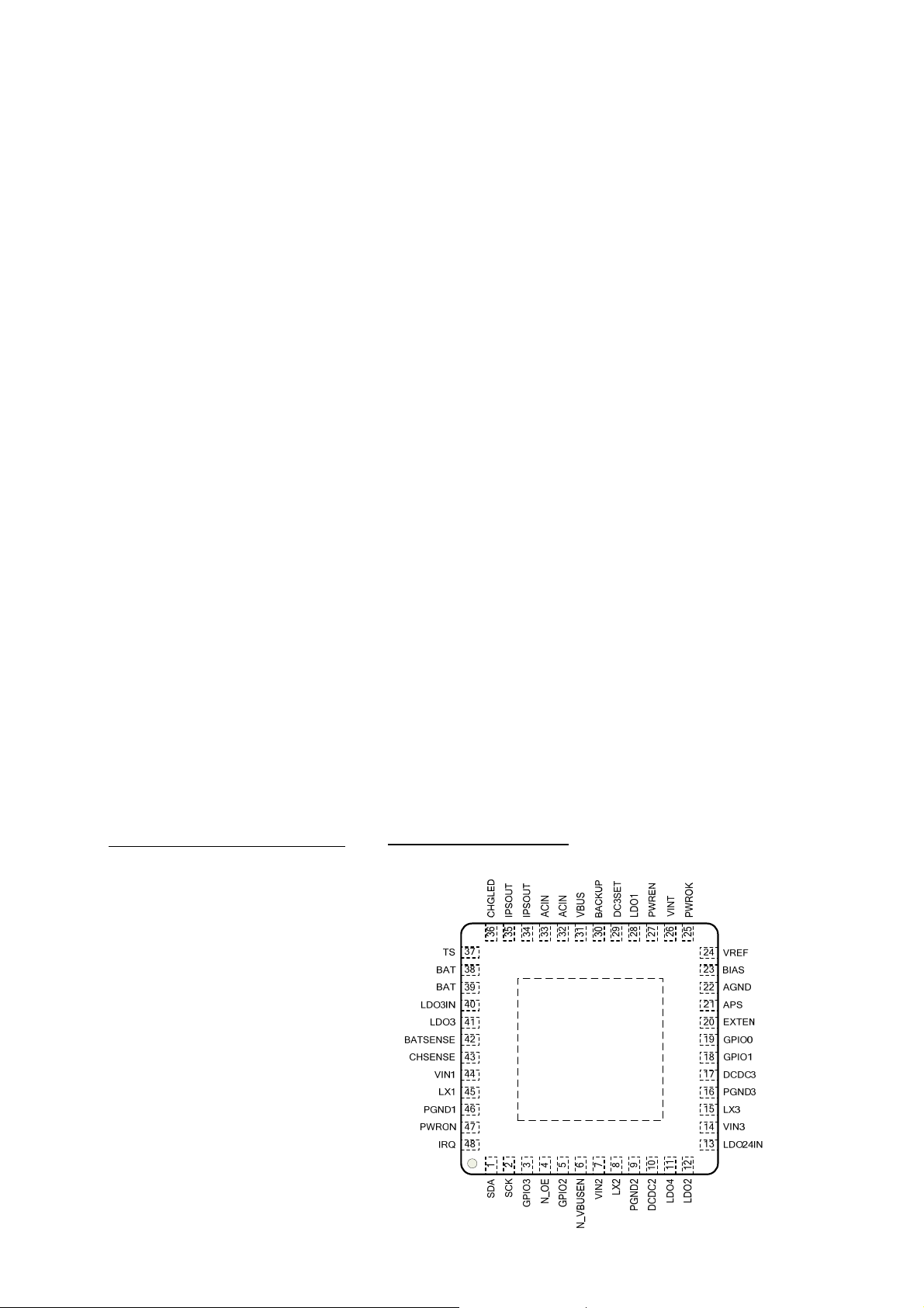
AXP202 is available in a 6mm x 6mm 48-pin QFN package.
Product Application
z Portable Handset:
Smartphone, PMP/MP4, Digital
Camera, Digital Camcorder,
PND, PDA, PTV
z Mobile Connected Devices
such as xPad,MID
z DPF, Portable DVD Player,
Ultra Mobile UMPC and
UMPC-like,Entertainment and
Education Machine
z Application Processor systems
z Other battery and multi-power
Pin Description
VQ.QW WPPIQPWE CC Confidential Page 2/48
www.x-powers.com
Page 3

AXP202
Single Cell Li-Battery PWM Charger and Power System Management IC
2. Feature
• Intelligent Power Select(IPS)
o W ide in pu t Voltage
2.9V~6.3V (AMR:-0.3V~11V)
o Configurable highefficient IPS system
o Adaptive USB(supporting USB3.0) or
AC-adaptor with voltage/current-limit
(4.4V/900mA/500mA/100mA)
o Equivelent Resistance of Batter Power Path
less than 75mΩ
• Fully Integrated PWM Cha rger
o Max Charge Current up to 1.8A
o Support Battery Temperature Monitoring
o Support USB compatible
charger( supporting USB3.0)
o Support Battery of Various Voltage such as
4.1V/4.15V/4.2V/4.36V
o Automatic Charge Procedure Management
o Directly drive LED to indicate charge
status
o Automatical scaling of charge current
according to the System Load
• Backup Battery
o Backup Battery to Supply Power for RTC
o Support Backup Battery Charge with
Adjustable Charge Current
• 2 Synchronous Duck DC-DC
o DC-DC1 : PWM Charger
o DC-DC2 : 1.6A ,with Voltage from 0.7V to
2.275V and 25mV/step, supporting Voltage
Ramp Control(VRC)
o DC-DC3 : 1.2A with Voltage from 0.7V to
3.5V and 25mV/step
• 5 Low-dropout Linear Regulator(LDO)
o LDO1:Always-on 30mA LDO1
o LDO2:200mA Low Noise with voltage
from 1.8V to 3.3V and 100mV/step
o LDO3:200mA with Voltage from 0.7V to
3.5V and 25mV/step
o LDO4:200mA Low Noise with voltage
from 1.8V to 3.3V and 100mV/step
o LDO5:50mA Low Noise with voltage from
1.8V to 3.3V and 100mV/step
VQ.QW WPPIQPWE CC Confidential Page 3/48
www.x-powers.com
• Signal Capture System
o 12 channel on-chip 12-bit ADC
o Support 2 external signal input
o Provide Battery and External Input Power Current
and Voltage
o On-chip Coulometer and Fuelgauge with High
Precision
o Provide Various Power Management data such as
Transient Power Consumption(mA or mW),
Remaining Battery Life(% or mAh),Charge State(%)
and Charge Time
o Two-level Low-Power Warning & Protection
o Provide AXP202 Die Temperature
• Host Interface
o Host can exchange data with PMIC via TWSI
o Flexible Interrupts and Sleep Management
o Flexible Pin Function Configuration. Multiple GPIO
can be set as IO, ADC and so on
o On-chip Configurable Timer
o 12 Registers for Data storage during System
Power-off
• System Management
o Support Soft Reset and Hard Reset
o Support Soft Power-off and Hard Power-off
o Support Exteranl Wakeup T r iggers
o Support Output Voltage Monitoring and
Self-Diagnosis
o Output PWROK indicating System Reset or
Power-off
o External Power
Detection(Plugin/Removal/Inqualified Drive
Capability)
o Support Soft Power-on for Input & Output
o Overvoltage/Undervoltage Protection(O V P/U V P)
o Overcurrent Protection(OCP)
o Overtemperature Protection(OTP)
o Support OTG VBUS Power State Setting/Monitoring
• Highly Integration
o Internal Reference Voltage with High Accuracy
(0.5%)
o On-chip MOSFET
o Customizable Timing and Output Voltage
Page 4
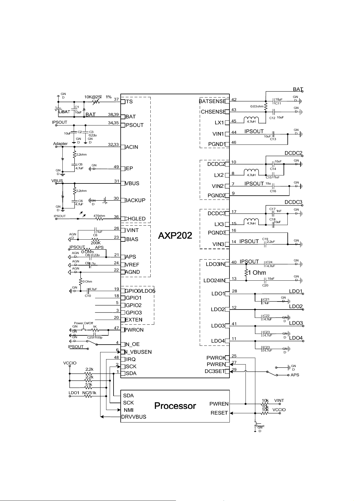
3. Typical Application
AXP202
Single Cell Li-Battery PWM Charger and Power System Management IC
VQ.QW WPPIQPWE CC Confidential Page 4/48
www.x-powers.com
Page 5
AXP202
Single Cell Li-Battery PWM Charger and Power System Management IC
4. Absolute Maximum Ratings
Symbol Description Value Units
ACIN Input Voltage -0.3 to 11 V
VBUS Input Voltage -0.3 to 11 V
TJ Operating Temperature Range -40 to 130
Ts Storage Temperature Range -40 to 150
T
V
LEAD
ESD
Maximum Soldering Temperature (at leads,10sec)
Maximum ESD stress voltage,Human Body Model
300
>4000 V
℃
℃
℃
PD Maximum Power Dissipation 2100 mW
5. Electrical Characteristics
VIN =5V, BAT=3.8V, TA= 25℃
SYMBOL DESCRIPTION CONDITIONS MIN TYP MAX UNITS
ACIN
VIN ACIN Input Voltage 3.8 6.3 V
I
V
OUT
Current Available Before
OUT
500mV Voltage Drop 2500 mA
Loading BAT
V
ACIN Under Voltage Lockout 3.8 V
UVLO
V
IPS Output Voltage 2.9 5.0 V
OUT
R
Internal Ideal Diode On
ACIN
Resistance
PIN to PIN, ACIN to
IPSOUT
170 mΩ
VBUS
VIN VBUS Input Voltage 3.8 6.3 V
I
V
OUT
Current Available Before
OUT
500 900 mA
Loading BAT
V
VBUS Under Voltage Lockout 3.8 V
UVLO
V
IPS Output Voltage 2.9 5.0 V
OUT
R
Internal Ideal Diode On
VBUS
Resistance
PIN to PIN, VBUS to
IPSOUT
300 mΩ
Battery Charger
V
BAT Charge Target Voltage -0.5% 4.2 +0.5% V
TRGT
I
Charge Current 1200 1800 mA
CHRG
I
Trickle Charge Current 10% I
TRKL
CHRG
mA
V
Trickle Charge Threshold
TRKL
3.0 V
Voltage
VQ.QW WPPIQPWE CC Confidential Page 5/48
www.x-powers.com
Page 6
AXP202
Single Cell Li-Battery PWM Charger and Power System Management IC
ΔV
T
TIMER1
Recharge Battery Threshold
RECHG
Voltage
Charger Safety Timer
Threshold Voltage
Relative to V
Trickle Mode 40 Min
Termination Time
T
Charger Safety Timer
TIMER2
CC Mode 480 Min
Termination Time
I
End of Charge Indication
END
CV Mode 10% 15% I
Current Ratio
Backup Battery
V
Backup Battery Charge Target
TRGT
2.5 3.0 3.1 V
Voltage
I
Backup Battery Charge
CHRG
50 200 400 uA
Current
I
Current when use Backup
Backup
10 15 uA
Battery
NTC
Charge 2.112 VTL Cold Temperature Fault
Threshold Voltage
Discharge
Charge 0.397 VTH Hot Temperature Fault
Threshold Voltage
VTE NTC Disable Threshold
Voltage
Discharge
Falling Threshold
Hysteresis
Ideal Diode
R
On Resistance(BAT to
ds(on)
75 mΩ
IPSOUT)
TAR GE T
-100 mV
CHRG
mA
0
3.264
V
3.226
0
3.264
V
0.282
0.2 V
SYMBOL DESCRIPTION CONDITIONS MIN TYP MAX UNITS
Off Mode Current
I
OFF Mode Current BAT=3.8V 27 μA
BATOFF
I
SUSPEND
USB VBUS suspend Mode
current
BAT=3.8V,
VBUS=5V,
86 μA
N_VBUSEN=1
Logic
VIL Logic Low Input Voltage 0.3 V
VIH Logic High Input Voltage 2 V
TWSI
VCC Input Supply Voltage 3.3 V
ADDRESS TWSI Address 0x68
f
Clock Operating Frequency 400 1200 kHZ
SCK
tf Clock Data Fall Time 2.2Kohm Pull High 60 ns
VQ.QW WPPIQPWE CC Confidential Page 6/48
www.x-powers.com
Page 7
AXP202
Single Cell Li-Battery PWM Charger and Power System Management IC
tr Clock Data Rise Time 2.2Kohm Pull High 100 ns
DCDC
f
Oscillator Frequency Default 1.5 MHz
OSC
DCDC2
I
PMOS Switch Current Limit PWM Mode 2300 mA
LIM2
I
V
DCDC3
I
I
V
SYMBOL DESCRIPTION CONDITIONS MIN TYP MAX UNITS
LDO1
V
Available Output Current PWM Mode 1800 mA
DC2OUT
Output Voltage Range
DC2OUT
PMOS Switch Current Limit PWM Mode 1400 mA
LIM3
Available Output Current PWM Mode 1000 mA
DC3OUT
Output Voltage Range
DC3OUT
Output Voltage I
LDO1
LDO1
=1mA
0.7 2.275
0.7 3.5
1.3
-1%
3.3
1%
V
V
V
I
Output Current 30 mA
LDO1
LDO2
V
Output Voltage I
LDO2
I
Output Current 200 mA
LDO2
PSRR Power Supply Rejection Ratio
=1mA 1.8 3.3 V
LDO2
=60mA,1KHz
I
LDO2
TBD dB
eN Output Noise,20-80KHz Vo=3V , Io=150mA 28 μV
LDO3
V
Output Voltage I
LDO3
I
Output Current 200 mA
LDO3
PSRR Power Supply Rejection Ratio
eN Output Noise,20-80KHz Vo=1.8V ,
=1mA 0.7 3.5 V
LDO3
=10mA, 1KHz
I
LDO3
TBD dB
TBD μV
Io=150mA
LDO4
V
Output Voltage I
LDO3
I
Output Current 200 mA
LDO3
PSRR Power Supply Rejection Ratio
eN Output Noise,20-80KHz Vo=1.8V ,
=1mA 1.8 3.3 V
LDO3
=10mA, 1KHz
I
LDO3
TBD dB
18 μV
Io=150mA
LDO5
V
Output Voltage I
LDO5
I
Output Current 50 mA
LDO5
PSRR Power Supply Rejection Ratio
=1mA 1.5 3.3 V
LDO5
=10mA,1KHz
I
LDO5
TBD dB
eN Output Noise,20-80KHz Vo=1.8V, Io=30mA 18 μV
RMS
RMS
RMS
RMS
VQ.QW WPPIQPWE CC Confidential Page 7/48
www.x-powers.com
Page 8
Single Cell Li-Battery PWM Charger and Power System Management IC
6. Typical Characteristics
DC-DC Efficiency vs. Load(3.8Vin)
AXP202
DC-DC Load Transient(Typical)
VQ.QW WPPIQPWE CC Confidential Page 8/48
www.x-powers.com
Page 9
AXP202
Single Cell Li-Battery PWM Charger and Power System Management IC
DC-DC Ripple
vs Temperature
V
REF
VQ.QW WPPIQPWE CC Confidential Page 9/48
www.x-powers.com
Page 10
AXP202
Single Cell Li-Battery PWM Charger and Power System Management IC
vs Temperature
V
TRGT
Off Mode Current vs V
BAT
VQ.QW WPPIQPWE CC Confidential Page 10/48
www.x-powers.com
Page 11

AXP202
Single Cell Li-Battery PWM Charger and Power System Management IC
7. Pin Description
Num Name Type Condition Function Description
1 SDA IO Data pin for serial interface,normally it connects a
2.2K resistor to 3.3V I/O power
2 SCK I the Clock pin for serial interface,normally it connects
a 2.2K resistor to 3.3V I/O power
3 GPIO3 IO
4 N_OE I Power output on/off switch
5 GPIO2 IO REG92H[2:0] GPIO 2
6 N_VBUSEN I VBUS to IPSOUT Selection
7 VIN2 PI DCDC2 input source
8 LX2 IO Inductor Pin for DCDC2
9 PGND2 G NMOS Ground for DCDC2
10 DCDC2 I DC-DC2 feedback pin
11 LDO4 O Output Pin of LDO4
REG9EH[7]
GPIO 3
GND:on; IPSOUT:off
GND:IPSOUT select VBUS
High:IPSOUT do not select VBUS
12 LDO2 O Output Pin of LDO2
13 LDO24IN PI Input to LDO2 and LDO4
14 VIN3 PI DCDC3 input source
15 LX3 IO Inductor Pin for DCDC3
16 PGND3 G NMOS GND for DCDC3
17 DCDC3 I Feed back to DCDC3
REG93H[2:0]
19 GPIO0 IO
REG90H[2:0]
20 EXTEN O
21 APS PI Internal Power Input
22 AGND G Analog Ground
23 BIAS IO External 200Kohm 1% resistor
24 VREF O Internal reference voltage
25 PWROK O Power Good Indication Output
26 VINT PO Internal logic power, 2.5V
27 PWREN IO It is the Power domain enable signal
28 LDO1 O
GPIO 1 18 GPIO1 IO
ADC Input
GPIO 0
Low noise LDO/Switch
ADC Input
External Power Enable
LDO1 output,for Host RTC block
VQ.QW WPPIQPWE CC Confidential Page 11/48
www.x-powers.com
Page 12

Single Cell Li-Battery PWM Charger and Power System Management IC
29 DC3SET IO It set the DCDC3 default voltage
30 BACKUP IO Backup battery pin
31 VBUS PI USB VBUS input
32,33
ACIN PI Adapter input
AXP202
34,35
36 CHGLED O Charger status indication
37 TS I Battery Temperature sensor input or external ADC
38,39
40 LDO3IN O LDO3 input source
41 LDO3 I
42 BATSENSE I PWM Charger Current sense port1
43 CHSENSE O PWM Charger Current sense port2
44 VIN1 PI PWM Charger input source
45 LX1 IO Inductor Pin for PWM Charger
46 PGND1 G NMOS Ground for PWM Charger
47 PWRON I Power On-Off key input
48 IRQ IO IRQ output
49 EP G Exposed Pad, need to connect to system ground
IPSOUT IO Main Battery
input
BAT PO System power source
Output Pin of LDO3
VQ.QW WPPIQPWE CC Confidential Page 12/48
www.x-powers.com
Page 13
Single Cell Li-Battery PWM Charger and Power System Management IC
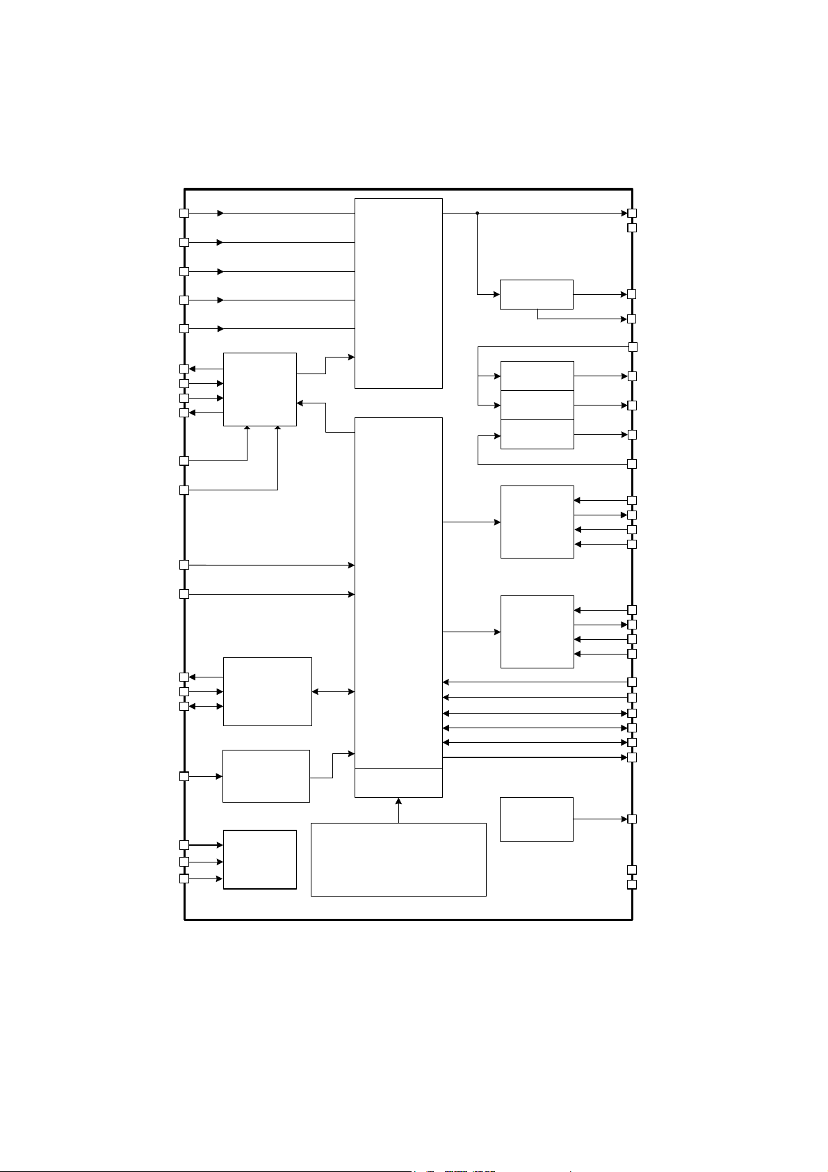
8. Functional Block Diagram
AXP202
VBUS
BAT
ACIN
N_VBUSEN
BACKUP
LX1
VIN1
PGND1
CHGLED
BATSENSE
CHSENSE
PWRON
N_OE
IRQ
SCK
SDA
TS
BIAS
VREF
VINT
PWM
Charger
Serial Interface
Bat
Temperature
Monitor
Reference
Voltage
IPS
Control Logic
Register
12 bit ADC
Current Monitor
Voltage Monitor
Temperature Monitor
LDO1
LDO2
LDO4
LDO3
DC-DC2
DC-DC3
Output
voltage
monitor/LBO
IPSOUT
APS
LDO1
N_RSTO
LDO24IN
LDO2
LDO4
LDO3
LDO3IN
DCDC2
LX2
VIN2
PGND2
DCDC3
LX3
VIN3
PGND3
DC3SET
PWREN
GPIO2
GPIO1
GPIO0/LDOio0
EXTEN
PWROK
AGND
EP
VQ.QW WPPIQPWE CC Confidential Page 13/48
www.x-powers.com
Page 14

AXP202
Single Cell Li-Battery PWM Charger and Power System Management IC
9. Control and Operation
Once AXP202 is powered on, SCK/SDA pin of TWSI will be pulled up to IO Power and then Host can
adjust and monitor AXP202.
Remarks: “Host” here refers to system processor.
Remarks: “External Power” below includes ACIN and VBUS input.
9.1 Power On/Off & Reset
Power Enable Key (PEK)
The Power Enable/ Sleep/Wakeup Key can be connected between PWRON pin and GND of AXP202.
AXP202 can automatically identify the “Long-press” and “Short-press” and then correspond
respectively.
Power on Source
1. ACIN、VBUS and battery
2. N_OE changes from high to low
3. PEK
Power On
System power-on is initiated whenever the following conditions occur:
1. N_OE is low and a valid power source has plugged in (ACIN or VBUS>3.8V, and battery voltage is
higher than power off voltage), AXP202 will be turned on. ( Developer can decide whether AXP202
shall be turned on when there is a valid power source plugging in)
2. N_OE is low and the system is powered off, press PEK can power on AXP202 (In application, Host
Alarm output signal can be connected to PWRON and parallel with PEK. Whenever there is a valid
Alarm signal ((Low Level)), AXP202 can be powered on).
3. When there is a external power source or battery, when N_OE changes from high to low, AXP202
will be turned on.
After power on, DC-DC and LDO will be soft booted in preset timing sequence, and then either Host or
PWREN pin can enable/disable corresponding power.
VQ.QW WPPIQPWE CC Confidential Page 14/48
www.x-powers.com
Page 15

AXP202
Single Cell Li-Battery PWM Charger and Power System Management IC
Power Off
When you push-and-hold PEK longer than IRQLEVEL, HOST can write “1” into“REG32H [7]” to inform
AXP202 to shutdown, which can disable all power output except LDO1.
System power-off is initiated whenever the following conditions occur:
1. input voltage is too low( Low-Power Protection)
2. Power output voltage is too low due to overload( Overload Protection)
3. Input voltage is too high( Overvoltage Protection)( See more details in chapter “ Intelligent Power
Select”
4. Have waited more than 2S(default) when N_OE changes from hight to low
5. Push PEK longer more than OFFLEVEL( Default 6S), and system will cut off all power output
except LDO1( there is no need for an extra RESET key)
Remarks: With the automatic protection mechanism, AXP202 can protect whole system by preventing
Components from irriversable damage due to system abnormality.
Sleep and wakeup
When the running system needs to enter Sleep mode, REG31H [3] will determine whether one or
several power rails should be disabled or change to other voltage. Wakeup can be triggled by either
PEK signal, or the rising/falling edge of GPIO0、GPIO1、GPIO2、GPIO3 (To be the rising or falling edge,
or both can be programmed by REG90H[7:6]、REG92H[7:6]、REG93H[7:6] and REG95H[7:6]), with all
power rails resume to default voltage in default power on timing sequence.
NOTE: PEK IRQ(REG42H[1])、GPIO0 INPUT Edge IRQ(REG44H[0])、GPIO1 INPUT Edge IRQ
(REG44H[1])、GPIO2 INPUT Edge IRQ(REG44H[2])、GPIO3 INPUT Edge IR(REG44H[3])should
be “Enable” to notify the processor to exit Sleep Mode via IRQ PIN.
See control process under sleep and wakeup modes as below:
VQ.QW WPPIQPWE CC Confidential Page 15/48
www.x-powers.com
Page 16

Single Cell Li-Battery PWM Charger and Power System Management IC
Write “1” to REG31H[3] to
start the sleep,and PMU will
save REG12H setting at that
time
Disable corresponding power
or modify the voltage
Sleep and wait to be Wakeup
N
AXP202
Wakeup?
Y
Restore the Power to the
default output voltage.
System Reset and Output Monitoring (PWROK)
The PWROK in AXP202 can be used as the reset signal of application system. During AXP202 startup,
PWROK outputs low level, which will then be pulled high to startup and reset the system after each
output voltage reaches the regulated value.
When application system works normally, AXP202 will be always monitoring the voltage and load
status. If overload or under-voltage occurs, the PWROK will instantly drive low to reset the system and
prevent data losses.
9.2 Power Path Management (IPS)
Power input of AXP202 may come from Li-battery, USB VBUS input, external power ACIN (such as
AC adapter). IPS can select proper power according to external power and Li-battery status.
o If only Li-battery is available, and no external power input, Li-battery is used for power input;
o If external power is available (VBUS or ACIN), it is preferred in power supply
VQ.QW WPPIQPWE CC Confidential Page 16/48
www.x-powers.com
Page 17

AXP202
Single Cell Li-Battery PWM Charger and Power System Management IC
o If Li-battery is available, it will “Seamlessly”switch to Li-battery once external power is removed
o When both VBUS and ACIN are available, ACIN will be applied to supply power in priority, and
Li-battery will be charged.
o If ACIN drive capability is not enough, VBUS will be enabled to achieve ACIN/VBUS common
power supply.
o If the drive capacity is still insufficient, charge current will be reduced to zero, and battery is
used for power supply.
Therefore, compatibility of the system with external powers of different drive ability can be
dramatically improved, and no special customized adapters are required to be provided on the part
of manufacturers.
Please refer to the following diagram.
As shown above, when ACIN provides insufficient load ability, IPSOUT voltage will fall, and BAT
will change from charge to discharge to supply load current together with ACIN.
Host can set IPS parameters and read the feedback by visiting internal registers in AXP202 via
TWSI.
Voltage-Limit/ Current-Limit Mode and Direct Mode
VQ.QW WPPIQPWE CC Confidential Page 17/48
www.x-powers.com
Page 18

AXP202
Single Cell Li-Battery PWM Charger and Power System Management IC
In order not to affect the USB communication, VBUS is always working under Voltage-Limit mode by
default. In this mode, AXP202 ensures that VBUS voltage remains above a configurable reference
voltage VHOLD which can meet the USB specification. The default VHOLD is 4.4V, adjustable in
Reg30H [5:3] register.
If the system has limit on current obtained from USB VBUS, a current-limit mode is provided (See
REG30H[1] register), with 900mA/500mA/100mA (Reg30H [0]) selectable.
If the system just utilizes the USB for power supply rather than communication, or the USB power
adapter is utilized, AXP202 can be set to “VBUS Direct Mode” by modifying register REG30H[6], and
then AXP202 will give priority to the application power demand. When the drive ability of USB Host is
insufficient or system power consumption is large then the VBUS voltage is lower than VHOLD,
AXP202 will release IRQ to indicate the weak power supply ability of Host VBUS, which may affect
USB communication, and then Host software will follow up.
AXP202’s Reaction to External Power Supply Plugin
AXP202 can automatically detect the plugin of external powersand judge whether the power is usable
or not. The result will be set in corresponding registers, and IRQ will be released to inform the Host at
the same time.
The following table has listed the status bits and meanings of external power registers.
Register Status
Bits
Description
REG00H[7] Indicating the presence of external ACIN
REG00H[6] Indicating whether the external ACIN is usable or not
REG00H[5] Indicating the presence of external VBUS
REG00H[4] Indicating whether the external VBUS is usable or not
REG00H[3] Indicating whether the VBUS voltage is above V
when used
HOLD
REG00H[1] Indicating whether ACIN/VBUS short circuits on PCB or not
REG00H[0] Indicating whether the system is triggered to startup by ACIN/VBUS
or not
The status bit of “indicating whether the VBUS voltage is above V
or not when used” enables the
HOLD
Host to judge when it receives IRQ7(indicating weak supply ability)whether VBUS is pulled low by
system load input or the external power itself is below V
, which may facilitate Host software to
HOLD
decide either to keep on working in Voltage-Limit mode or switch to Direct mode.
When to Select VBUS as Input Power
N_VBUSEN and register REG30H[7]: is used to determined when shall VBUS be used as power
VQ.QW WPPIQPWE CC Confidential Page 18/48
www.x-powers.com
Page 19

AXP202
Single Cell Li-Battery PWM Charger and Power System Management IC
supply.
N_VBUSEN REG30H[7] Input Power Description
Low 0 VBUS Select if VBUS is valid and no ACIN is
available
Low 1 VBUS
High 1 VBUS
High 0 ACIN/BAT Not select VBUS
Low-Power Warning and Low-Power Protection (Automatic Poweroff)
With AXP202, the value of V
WARNING
(low-power warning voltage) and V
can be set. If the system power is found to be lower than V
APS is lower than V
AXP202 will automatically enter Shutdown Mode, and disable all other outputs
OFF,
except LDO1.
There are two-levels in V
WARNING
, namely, LEVEL 1 and LEVEL 2, which can be defined differently in
applications. For example, use LEVEL1 to indicate insufficient power while LEVEL 2 can be used to
indicate the oncoming shutdown.
The default values of V
WARNING
and V
can be respectively set in registers REG3AH、REG3BH and
OFF
REG31H[2:0].
Over-Voltage Protection
If the external power voltage exceeds 6.3V, AXP202 will release IRQ1/4 for indication. If the external
power voltage exceeds 7V, AXP202 will automatically shutdown the system.
select if VBUS is valid
(automatic shutdown voltage)
OFF
WARNING,
IRQ19/IRQ20 will be released. If
9.3 Adaptive PWM Charger
AXP202 integrates a constant current/voltage PWM charger to automatically control the charge cycle,
with a built-in safety clock capable of automatic charge termination without processor intervention. This
charger features automatic charge current scaling in accordance with the system power consumption,
as well as battery detection, trickle charge and activation. In addition, the built-in temperature detection
circuit can automatically decrease the charge current when the temperature is too high or too low.
Compared with traditional linear charge, this PWM charger features dramatic efficiency increase and
power consumption decrease in systems that require large power consumption and fast battery
charging, and thus greatly improve the system temperature performance.
Adaptive Charge Startup
VQ.QW WPPIQPWE CC Confidential Page 19/48
www.x-powers.com
Page 20

AXP202
Single Cell Li-Battery PWM Charger and Power System Management IC
The default state of the charger is “Enable”. (It can be programmed via registers. Refer to register
REG33H.) When external power is plugged in, AXP202 will firstly judge whether it is chargeable. If the
charger is suitable for the power, and the charge function is usable, AXP202 will automatically start the
charge, and send IRQ to Host for indication. At the same time, GHGLED pin will output low level to
drive external LED to indicate the charging state.
Charge Voltage/Current:
V
TRGT
I
CHRG
V
TRKL
I
TRKL
Two Symbolic Voltages
=charge target voltage. The V
V
TRGT
is 4.2V by default, which can be set by register (Refer
TRGT
to“REG33H[6:5]”) . At the same time, AXP202 will automatically adjust the charge target voltage when
external power voltage is low.
V
=automatic recharge voltage. V
RCH
RCH=VTRGT
-0.1V。
Charge Current
The charge current is 500mAor 1200mA by default, which can be set by REG33H [3:0].
Charge Process
If the battery voltage is lower than 3.0V, the charger will automatically enter the pre-charge mode, with
charge current be 1/10 of the preset value. If the battery voltage is still below 3.0V 40 minutes later
(adjustable, see “REG34H”), charger will automatically enter the battery activate mode. Refer to
“Battery Activate Mode” section for details.
VQ.QW WPPIQPWE CC Confidential Page 20/48
www.x-powers.com
Page 21

AXP202
Single Cell Li-Battery PWM Charger and Power System Management IC
Once the battery voltage exceeds 3.0V, the charger enters constant current mode. If the charge current
is below 65% of the preset value, the system will release IRQ17 to indicate that “drive ability of external
power is insufficient, as a result, the charge current is lower than the preset value, which may lead to
longer charge time, so stronger power is preferred, or the power-consuming functions should be
disabled to shorten the charge time.”
When the battery voltage reaches the V
constant voltage mode, and the charge current will fall.
When the charge current is lower than 10% or 15% (adjustable, see register “REG33H”) of the preset
value, a charge cycle ends, and AXP202 will release IRQ18 while the CHGLED pin will stop indicating
the charging state. When the battery voltage is below V
IRQ17 will be released.
In non-precharge mode, if the charge cycle is not ending after 480 minutes (adjustable, refer to register
“REG34H”), the charger will automatically enter the battery activate mode.
Battery Activate Mode
At the enterring the battery activate mode from either pre-charge mode or constant current mod(the
timer expires), AXP202 will release IRQ10 in both cases to indicate that the battery may be damaged.
In battery activate mode, the charger always inputs relatively low current to batteries. AXP202 will exit
activate mode and release IRQ11 only if the battery voltage has reached V
AXP202 will indicate whether the charger is in battery activate mode or not in register REG01H.
CHGLED
CHGLED pin is used to indicate charge state and warning. There are four states, namely, charging, not
charging, battery abnormal warning, and external power over-voltage warning. CHGLED is NMOS
Open Drain output, so a LED can be directly driven by a current-limit resistor to show the four states.
The following table has displayed its two operation modes.
the charger will switch from the constant current mode to
TRGT,
again, the automatic charge will restart, and
RCH
RCH.
REG34H[4] Status Performance Remark
0
Charging Low Level
Not charging High
Resistance
Battery
Abnormal
1Hz flicker The charger enters the battery activate mode, or
the battery temperature is too high/low.
Over-Voltage 4Hz flicker External voltage input is too high.
Charging 1Hz flicker 1
Non-chargeable High No external power is available.
VQ.QW WPPIQPWE CC Confidential Page 21/48
www.x-powers.com
Page 22

AXP202
Single Cell Li-Battery PWM Charger and Power System Management IC
Resistance
Not charging Low Level
Over-Voltage 4Hz Flicker External voltage input is too high, or the battery
temperature is too high/low.
Battery Temperature Detection
AXP202 can connect a temperature-sensitive resistor via the TS pin to monitor the battery
temperature when the battery is charging or discharging. The diagram is shown below.
BAT
10uF
C2
NTC
TS
GND
In the diagram above, VTH/VTL refer to the high temperature threshold and low temperature threshold,
which is programmable via registers REG38H/39H/3CH/3DH respectively. VTE=0.2V. The
temperature-sensitive resistor is suggested to choose the NTC temperature-sensitive resistor, which is
10Kohm and 1% accuracy at 25℃. AXP202 will send constant current via TS pin, and the current can
be set as 20uA、40uA、60uA、and 80uA (See registerREG84H) to adapt to different NTC resistors.
When the current goes through the temperature-sensitive resistor, a test voltage is generated, which
will be measured by ADC, and compared with regulated value to release corresponding IRQ or
suspend the charge.
If the resistance value of temperature-sensitive resistor is too high or too low, extra resistors can be
serial or parallel connected to expand the detect extent.
If the battery is free from temperature-sensitive resistor, TS pin can be linked to the ground, and in that
case, AXP202 will automatically disable the battery temperature monitoring function.
Battery Detection
VQ.QW WPPIQPWE CC Confidential Page 22/48
www.x-powers.com
Page 23

AXP202
Single Cell Li-Battery PWM Charger and Power System Management IC
AXP202 will automatically detect the battery presence, record the result in registers (refer to REG01H)
and release IRQ13, IRQ14.
The battery detection can be enabled and disabled by Host. (Refer to register REG32H.)
9.4 Backup Batttery
AXP202 supports backup battery charge and discharge. When no main power (BAT/ACIN/VBUS) is
available, LDO1 will choose the backup battery to support the operation of some circuits, such as the
system real-time clock, etc.
When there is a main power, REG35H[7] can be set to charge the backup battery, whose target voltage
is 3.0V by default (adjustable via REG35H[6:5]) and charge current is 200uA by default ( adjustable via
REG35H[1:0]).
9.5 Multi-Power Outputs
The following table has listed the multi-power outputs and their functions of AXP202.
Output Path Type
DCDC2 BUCK Configurable 1.25Vcore 1800 mA
DCDC3 BUCK Configurable 2.5Vddr 1000 mA
LDO1 LDO Configurable RTC 30 mA
LDO2 LDO Configurable Analog/FM 200 mA
LDO3 LDO Configurable 1.3V PLL 200 mA
LDO4 LDO Configurable 1.8V HDMI 200 mA
LDO5 LDO Configurable Vmic 50 mA
AXP202 comes with two synchronous step-down DC-DCs, five LDOs, as well as multiple timing and
controlling methods. The work frequency of DC-DC is 1.5MHz by default, which is adjustable via
registers. External small inductors and capacitors can be connected as well. In addition, both DC-DCs
can be set in PWM mode or auto mode (automatically switchable according to the AXP202 load). See
register REG80H.
DC-DC2/3
DCDC3 output voltage ranges from 0.7 V to 3.5V,and output voltage of DCDC2 is ranged from
0.7-2.275V,which can be programmed via registers.(refer to “ register REG23H 27H”).
DCDC2/3 output capacitor is recommended to use small ESR ceramic capacitors above 10uF X7R;
Default
Voltage
Application
Examples
Drive Ability
VQ.QW WPPIQPWE CC Confidential Page 23/48
www.x-powers.com
Page 24

AXP202
Single Cell Li-Battery PWM Charger and Power System Management IC
when the output voltage is set above 2.5V,2.2uH inductors is recommended; when the output voltage
is set under 2.5V,4.7uH inductors is recommended. Besides, the inductor saturation current should be
larger than 50% of the largest demanded current in power circuitry.
Inductor Recommendation List:
Inductors
Module NO. Current Spec DC Internal Resistance
Murata LQH55PN2R2NR0 2100mA@2.2uH 30mOhm
Murata LQH55PN4R7NR0 1400mA@4.7uH 60mOhm
Murata LQH44PN2R2MP0 2000mA@2.2uH 49mOhm
Murata LQH44PN4R7MP0 1700mA@2.2uH 80mOhm
TDK VLF5010ST-2R2M2R3 2700mA@2.2uH 41mOhm
TDK VLF5014ST-4R7M1R7 1700mA@4.7uH 98mOhm
TDK
SLF6045T-4R7N2R4-3PF
2400mA@4.7uH 27mOhm
Capacitors
Module NO. Temperature spec Allowance
TDK C2012X5R0J475K X5R/X7R 10%@4.7uF
TDK C2012X5R0J106K X5R/X7R 10%@10uF
Murata GRM31E71A475K X7R 10%@4.7uF
Murata GRM21E71A106K X7R 10%@10uF
Murata GRM31E71A106K X7R 10%@10uF
LDO 1
LDO1 is always on and can be used to supply continuous power for application RTC with 30mA drive
ability 30mA.
LDO2/3/4
LDO2/4 output noise is as low as 18uVrms,and can be used to supply power for analog circuits of
application system. LDO3 can supply power for systems like SRAM or PLL with 200mA drive ability.
LDO5
LDO5 also features the low noise design, and its drive ability is 50mA。
Soft Start
All DC-DCs and LDOs support soft start which can avoid the impact of dramatic current change on
the input path in system boot stage.
Self-Diagnosis: Load Monitoring and Current-Limit Protection
VQ.QW WPPIQPWE CC Confidential Page 24/48
www.x-powers.com
Page 25

AXP202
Single Cell Li-Battery PWM Charger and Power System Management IC
All DC-DCs and LDOs support load monitoring and current-limit functions. When the load current
exceeds its drive ability, all output voltage will decrease to protect the internal circuits. When the two
DC-DCs output voltage is lower than 85% of the set voltage, AXP202 will automatically shutdown. At
the same time, the system will record the detailed output voltage that has lead to automatic shutdown
(refer to register REG46H[5:2]) and release corresponding IRQ.
All DC-DCs do not require external Schottky diodes and resister divider feedback circuits. If a certain
DC-DC is unnecessary in application, just float the corresponding LX pins.
9.6 Default Voltage/Timing Setting
The default voltage and boot timing of each power can be set by AXP202.
Boot Timing includes eight levels, and the interval between each level can be set as 1、4、16 and
32mS.
Default voltage setting: each DC-DC/LDO setting ranges from the lowest voltage to the highest
voltage.
DC3SET PIN is used to set the prelimirary voltage of DC-DC3:
DC3SET DC3SETGND DC3SETto OAPS DC3SET floating
DC-DC3 voltage 1.8V 3.3V/2.5V 1.2V/1.5V
9.7 Signal Capture
Ordinary battery monitor estimate the battery energy by measuring the battery voltage. However, the
multiple 12-bit ADCs in AXP202 can measure battery voltage, as well as battery current and external
power voltage and current. It also integrates battery charge and discharge coulomb counter. According
to these data, Host is capable of calculating accurately the battery energy and other battery data, such
as the system real-time consumption, remaining battery energy, battery charge progress, remaining
battery using time and charge time, etc.
The Enable state controlling and sampling rate of each ADC can be set via registers REG82H、83H、
84H. The sampling results will be saved in corresponding registers,and reference can be made to the
ADC data in Register Instruction section. The input range of GPIO[1:0] can be set via register REG85H
while register REG00H[2] is used to indicate the battery charge/discharge current directions.
Channel 000H STEP FFFH
Battery Voltage 0mV 1.1mV 4.5045V
Bat discharge current 0mA 0.5mA 4.095A
VQ.QW WPPIQPWE CC Confidential Page 25/48
www.x-powers.com
Page 26

AXP202
Single Cell Li-Battery PWM Charger and Power System Management IC
Bat charge current 0mA 0.5mA 4.095A
ACIN volatge 0mV 1.7mV 6.9615V
ACIN current 0mA 0.625mA 2.5594A
VBUS voltage 0mV 1.7mV 6.9615V
VBUS current 0mA 0.375mA 1.5356A
Internal temperature -144.7℃ 0.1℃ 264.8℃
APS voltage 0mV 1.4mV 5.733V
TS pin input 0mV 0.8mV 3.276V
GPIO0 0/0.7V 0.5mV 2.0475/2.7475V
GPIO1 0/0.7V 0.5mV 2.0475/2.7475V
9.8 Multi-Function Pin Description
GPIO[3:0]
Can be defined as GPIO[3:0], ADC Input(monitoring external signals), or LDO, etc. Please refer to
REG90H-96H Instruction for details
CHGLED
Features charge state indication, over-temperature/over-voltage warning, and GPO. Please refer to
REG32H Instruction section for details.
9.9 Timer
AXP202 features a 7-bit internal timer, whose values can be programmed via register
REG8AH[6:0]. The minimum time step of timer is one minute, and the timing range is 1~127 minutes.
VQ.QW WPPIQPWE CC Confidential Page 26/48
www.x-powers.com
Page 27

9.10 TWSI and IRQ
AXP202
Single Cell Li-Battery PWM Charger and Power System Management IC
…
… …
…
…
Fig.1: Single Read and Write
… …
…
…
…
… …
…
…
Fig.2:Multi Read and Write
Host can visit AXP202 registers via the TWSI interface, and the operation timing is listed above.
VQ.QW WPPIQPWE CC Confidential Page 27/48
www.x-powers.com
Page 28

AXP202
Single Cell Li-Battery PWM Charger and Power System Management IC
Standard 100KHz or 400KHz frequency is supported, and the highest rate can reach 1.2KHz. In
addition, multi read and write operation is supported, and the device addresses are 69H (READ) and
68H (WRITE).
When certain events occur, AXP202 will inform Host by pulling down the IRQ interrupt mechanism, and
the interrupt state will be reserved in interrupt state registers (See registers REG48H, REG49H,
REG4AH, REG4BH and REG4CH). The interrupt can be cleared by writing 1 to corresponding state
register bit. When there is no interrupt, IRQ output will be pulled high (51K resistance higher through
the external). Each interrupt can be masked via interrupt control registers (Refer to registers REG40H,
REG41H, REG42H, REG43H, and REG44H).
REG IRQ Description REG IRQ Description
REG48H[7] IRQ1 ACIN Over voltage REG 4AH[3] IRQ20 DCDC3 voltage too
long
REG 48H[6] IRQ2 ACIN plug in REG 4AH[2] Reserved
REG 48H[5] IRQ3 ACIN removal REG 4AH[1] IRQ22 PEKshort-press
REG 48H[4] IRQ4 VBUS Over voltage REG 4AH[0] IRQ23 PEK long-press
REG 48H[3] IRQ5 VBUS plug in REG 4BH[7] IRQ24 N_OE Power on
REG 48H[2] IRQ6 VBUS removal REG 4BH[6] IRQ25 N_OEPower off
REG 48H[1] IRQ7 VBUS voltage lower
than V
HOLD
REG 48H[0] Reseverd REG 4BH[4] IRQ27 VBUS Invalid
REG 49H[7] IRQ8 Battery plugin REG 4BH[3] IRQ28 VBUS Session Valid
REG 49H[6] IRQ9 Battery Removal REG 4BH[2] IRQ29 VBUS Session End
REG 49H[5] IRQ10 Enter battery
activate mode
REG 49H[4] IRQ11 Exit battery activate
mode
REG 49H[3] IRQ12 charging REG 4CH[7] IRQ32 Timer interrupt
REG 49H[2] IRQ13 Charge Done REG 4CH[6] IRQ33 PEK rising edge
REG 49H[1] IRQ14 Battery temp toor
high
REG 49H[0] IRQ15 Battery temp too low REG 4CH[4] Reserved
REG 4AH[7] IRQ16 Die Temp too high REG 4CH[3] IRQ35 GPIO3 input edge
REG 4AH[6] IRQ17 Charge current
insufficient
REG 4AH[5] IRQ18 DCDC1voltage too
long
REG 4AH[4] IRQ19 DCDC2 voltage too
long
REG 4BH[5] IRQ26 VBUS Valid
REG 4BH[1] IRQ30 Low power LEVEL1
REG 4BH[0] IRQ31 Low power LEVEL2
REG 4CH[5] IRQ34 PEK falling edge
trigger
REG 4CH[2] IRQ36 GPIO2 input edge
trigger
REG 4CH[1] IRQ37 GPIO1 input edge
trigger
REG 4CH[0] IRQ38 GPIO0 input edge
trigger
VQ.QW WPPIQPWE CC Confidential Page 28/48
www.x-powers.com
Page 29

Single Cell Li-Battery PWM Charger and Power System Management IC
10. Registers
Group 1: Power Control
Address Register Description R/W Default
00 Power status register R
01 Power mode/ charge state register R
02 OTG VBUS state register R
04-0F Data buffer register R/W 00H
12 DC-DC2/3 & LDO2/3/4&EXTEN control register R/W XXH
23 DC-DC2 voltage setting register R/W XXH
25 DC-DC2/LDO3 voltage ramp parameter setting
register
27 DC-DC3 voltage setting register R/W XXH
28 LDO2/3 voltage setting register R/W XXH
30 VBUS-IPSOUT channel setting register R/W 60H
31 V
32 Shutdown, battery detection, CHGLED control
33 Charge control register1 R/W CXH
34 Charge control register2 R/W 41H
35 Backup battery charge control register R/W 22H
36 PEK parameter control register R/W 5DH
37 DCDC converter work frequency setting register R/W 08H
38 Battery charge under-temperature warning setting
39 Battery charge over-temperature warning setting
3A APS low-power Level1 setting register R/W 68H
3B APS low-power Level2 setting register R/W 5FH
3C Battery discharge under-temperature warning setting
3D Battery discharge over-temperature warning setting
register
80 DCDC work mode setting register R/W E0H
82 ADC enable setting register1 R/W 83H
83 ADC enable setting register2 R/W 80H
shutdown voltage setting register R/W X3H
OFF
register
register
register
register
R/W 00H
R/W 46H
R/W A5H
R/W 1FH
R/W FCH
R/W 16H
AXP202
Value
VQ.QW WPPIQPWE CC Confidential Page 29/48
www.x-powers.com
Page 30

AXP202
Single Cell Li-Battery PWM Charger and Power System Management IC
84
85 GPIO [1:0] input range setting register R/W X0H
86 GPIO1 ADC IRQ rising edge threshold setting R/W FFH
87 GPIO1 ADC IRQ falling edge threshold setting R/W 00H
8A Timer control register R/W 00H
8B VBUS monitoring setting register R/W 00H
8F Over-temperature shutdown control register R/W 01H
Group 2 GPIO control
Address Register Description R/W Default
90 GPIO0 control register R/W 07H
91 LDO5 output voltage setting register R/W A0H
92 GPIO1 control register R/W 07H
93 GPIO2 control register R/W 07H
94 GPIO[2:0] signal status register R/W 00H
95 GPIO3 control register R/W 00H
ADC sample rate setting,TS pin control register
R/W 32H
Value
Group3 Interrupt control
Address Register Description R/W Default
40 IRQ enable control register1 R/W D8H
41 IRQ enable control register2 R/W FFH
42 IRQ enable control register3 R/W 3BH
43 IRQ enable control register4 R/W C1H
44 IRQ enable control register5 R/W 00H
48 IRQ status register1 R/W 00H
49 IRQ status register2 R/W 00H
4A IRQ status register3 R/W 00H
4B IRQ status register4 R/W 00H
4C IRQ status register5 R/W 00H
Group4 ADC data
Address Register Description R/W
56[7:0] ACIN voltage ADC data high 8 bits R
57[3:0] ACIN voltage ADC data low 4 bits R
58[7:0] ACIN current ADC data high 8 bits R
59[3:0] ACIN current ADC data low 4 bits R
5A[7:0] VBUS voltage ADC data high 8 bits R
Value
VQ.QW WPPIQPWE CC Confidential Page 30/48
www.x-powers.com
Page 31

AXP202
Single Cell Li-Battery PWM Charger and Power System Management IC
5B[3:0] VBUS voltage ADC data low 4 bits R
5C[7:0] VBUS current ADC data high 8 bits R
5D[3:0] VBUS current ADC data low 4 bits R
5E[7:0] AXP202 internal temperature monitoring ADC data high 8 bits R
5F[3:0] AXP202 internal temperature monitoring ADC data low 4 bits R
62[7:0]
63[3:0]
64[7:0] GPIO0 voltage ADC data high 8 bits R
65[3:0] GPIO0 voltage ADC data low 4 bits R
66[7:0] GPIO1 voltage ADC data high 8 bits R
67[3:0] GPIO1 voltage ADC data low 4 bits R
70[7:0] Battery instantaneous power high 8 bits R
71[7:0] Battery instantaneous power middle 8 bits R
72[7:0] Battery instantaneous power low 8 bits R
78[7:0] Battery voltage high 8 bits R
79[3:0] Battery voltage low 4 bits R
7A[7:0] Battery charge current high 8 bits R
7B[3:0] Battery charge current low 4 bits R
7C[7:0] Battery discharge current high 8 bits R
7D[4:0] Battery discharge current low 5 bits R
7E[7:0] System IPSOUT voltage high 8 bits R
7F[3:0] System IPSOUT voltage low 4 bits R
TS input ADC data high 8 bits,default monitoring battery
temperature
TS input ADC data low 4 bits,default monitoring battery
temperature
R
R
Note: the battery power formula:
Pbat =2* register value * Voltage LSB * Current LSB / 1000.
(Voltage LSB is 1.1mV; Current LSB is 0.5mA, and unit of calculation result is mW.)
Address Register Description R/W Default
Value
B0 Battery charge coulomb counter data register[31:24] R/W 00H
B1 Battery charge coulomb counter data register[23:16] R/W 00H
B2 Battery charge coulomb counter data register[15:8] R/W 00H
B3 Battery charge coulomb counter data register[7:0] R/W 00H
B4 Battery discharge coulomb counter data
register[31:24]
B5 Battery discharge coulomb counter data
register[23:16]
B6 Battery discharge coulomb counter data
register[15:8]
B7 Battery discharge coulomb counter data register[7:0] R/W 00H
VQ.QW WPPIQPWE CC Confidential Page 31/48
R/W 00H
R/W 00H
R/W 00H
www.x-powers.com
Page 32

AXP202
Single Cell Li-Battery PWM Charger and Power System Management IC
B8 Coulomb counter control register R/W 00H
B9 FuelGuage result register R/W 00H
Coulomb calculation formula:
C= 65536 * current LSB *(charge coulomb counter value - discharge coulomb counter value) /
3600 / ADC sample rate. Refer to REG84H setting for ADC sample rate;the current LSB is
0.5mA;unit of the calculation result is mAh. )
REG 00H: Power Input Status
Bit Descripiton R/W
7 ACIN presence indication
0:ACIN not exist;1:ACIN exists
6 Indicating whether ACIN is usable R
5 VBUS presence indication
0:VBUS not exist;1:VBUS exists
4 Indicating whether VBUS is usable R
3 Indicating whether the VBUS voltage is above V
2 Indicating the battery current direction
0: the battery is discharging;1: the battery is charging
1 Indicating whether ACIN and VBUS input short circuit on PCB R
0 Indicating whether the boot source is ACIN or VBUS
0: Boot source isn’t ACIN/VBUS; 1: Boot source is ACIN/VBUS.
before used. R
HOLD
R
R
R
R
REG 01H: Power Working Mode and Charge Status Indication
Bit Descripiton R/W
7 Indicating whether AXP202 is over-temperature
0: not over-temperature; 1: over-temperature
6 Charge indication
0:not charge or charge finished; 1: in charging
5 Battery existence indication
0:no battery connected to AXP202; 1:battery already connected to AXP202
4 Reserved and unchangeable R
3 Indicating whether the battery enters the activate mode
0: not enter the activate mode; 1: already entered the activate mode
2 Indicating whether the charging current is lower than the expected current
0:actual charging current is the same as expected current; 1: actual charging current
is lower than expected current
1-0 Reserved and unchangeable R
R
R
R
R
R
VQ.QW WPPIQPWE CC Confidential Page 32/48
www.x-powers.com
Page 33

AXP202
Single Cell Li-Battery PWM Charger and Power System Management IC
REG 02H:USB OTG VBUS Status Indication
Bit Descripiton R/W
7-3 Reserved and unchangeable
Indicating whether VBUS is valid or not,1 means “valid”
2
Indicating whether VBUS Session A/B is valid,1 means “valid”
1
Indicating Session End status,1 means “valid”
0
REG 04-0FH: Data Cache
Note: As long as one of the external powers, batteries or backup batteries exists, this data will be
reserved and free from the startup and shutdown influence.
R
R
R
REG 12H: Power Output Control
Default Value:XXH
Bit Descripiton R/W Default
Value
7 Reserved and unchangeable RW X
6 LDO3 enable and disable control
5 Reserved and unchangeable RW X
4 DC-DC2 enable and disable
control
3 LDO4 enable and disable control RW X
2 LDO2 enable and disable control RW X
1 DC-DC3 enable and disable
control
0 EXTEN enable and disable control
0: disable; 1: enable
0: disable; 1: enable
RW X
RW X
RW X
RW X
REG 23H:DC-DC2 Output Voltage Setting
Default Value: XXH
Bit Descripiton R/W Default
Value
7-6 Reserved and unchangeable
5-0 DC-DC2 output voltage setting
[5:0]
VQ.QW WPPIQPWE CC Confidential Page 33/48
0.7-2.275V,25mV/step
Vout=[0.7+(Bit5-0)*0.025]V
RW X
www.x-powers.com
Page 34

AXP202
Single Cell Li-Battery PWM Charger and Power System Management IC
REG 25H:DC-DC2/LDO3 Dynamic Voltage Scaling Parameter Setting
Default Value:00H
Bit Description R/W Default
Value
7-4 Reserved and unchangeable
3 LDO3 VRC ENABLING CONTROL
0: enable; 1: disable
2 DC-DC2 VRC enabling control
0: enable; 1: disable
1 LDO3 VRC voltage rising slope
control
0 DC-DC2 VRC voltage rising slope
control
0: 25mV/15.625us=1.6mV/us
1: 25mV/31.250us=0.8mV/us
0: 25mV/15.625us=1.6mV/us
1: 25mV/31.250us=0.8mV/us
RW 0
RW 0
RW 1
RW 0
REG 27H:DC-DC3 Output Voltage Setting
Default Value: XXH
Bit Description R/W Default
Value
7 Reserved and unchangeable
6-0 DC-DC3 output voltage setting
0.7-3.5V, 25mV/step
Vout=[0.7+(Bit6-0)*0.025]V
RW X
REG 28H:LDO2/4 Output Voltage Setting
Default Value: XXH
Bit Description R/W Default
Value
7-4 LDO2 output voltage setting
3-0 LDO4 output voltage setting 1.25 1.3 1.4 1.5 1.6 1.7 1.8 1.9 2.0 2.5
1.8-3.3V, 100mV/step
Vout=[1.8+(Bit7-4)*0.1]V
2.7 2.8 3.0 3.1 3.2 3.3
RW X
RW X
REG 29H:LDO3 Output Voltage Setting
Default Value: XXH
VQ.QW WPPIQPWE CC Confidential Page 34/48
www.x-powers.com
Page 35

AXP202
Single Cell Li-Battery PWM Charger and Power System Management IC
Bit Description R/W Default
Value
LDO3 Mode select:
7
0:LDO mode,voltage can be set by [6:0]
1:enable/disable control mode,and voltage is determined by LDO3IN.
6-0 LDO3 output voltage setting
Bit6-Bit0
0.7-2.275V,25mV/step
Vout=[0.7+(Bit6-0)*0.025]V
REG 30H:VBUS-IPSOUT Power Path Management
Default Value: 6XH
Bit Description R/W Default
7 the VBUS-IPSOUT path select control signal when VBUS is usable
0: whether to enable the path is decided by N_VBUSEN pin
1:VBUS-IPSOUT can be enabled,regardless of the N_VBUSEN status
6 VBUS V
0: not limit the voltage; 1: limit the voltage
5-3 V
setting V
HOLD
2 Reserved and unchangeable
voltage-limit control
HOLD
= [4.0+(Bit5-3)*0.1]V RW 100
HOLD
RW 0
RW X
Value
RW 0
RW 1
1-0 VBUS current-limit selection when current-limit is enabled
RW 0
00:900mA ; 01:500mA; 10:100mA; 11:not limit
REG 31H:V
Power off Voltage Setting
OFF
Default Value: X3H
Bit Description R/W Default
Value
7-4 Reserved and unchangeable
3 PEK or GPIO edge wakeup function enable setting in Sleep mode
0:disable
1:enable
This bit will be automatically cleared to 0 after writing,so “1 ”should be
rewritten whenever enters the Sleep mode.
2-0 V
setting V
OFF
=[2.6+(Bit2-0)*0.1]V
OFF
RW 011
Default: 2.9V
VQ.QW WPPIQPWE CC Confidential Page 35/48
www.x-powers.com
Page 36

AXP202
Single Cell Li-Battery PWM Charger and Power System Management IC
REG 32H: Shutdown Setting, Battery Detection and CHGLED Pin Control
Default Value: 46H
Bit Description R/W Default
Value
7 Shutdown Control
Writing “1” to this bit will disable the AXP202 output.
Battery monitoring function setting bit: 0: disable; 1: enable
6
5-4 CHGLED pin function setting 00: high resistance
01: 25% 1Hz flicker
10: 25% 4Hz flicker
11: low level output
3 CHGLED pin control setting 0: controlled by charging
1: controlled by register REG 32H[5:4]
2 Output disable timing control 0: disable at the same time
1: contrary to the startup timing
1-0 the delayed shutdown time of
AXP202 after N_OE changes from
low to high
00: 128mS; 01: 1S;
10: 2S; 11: 3S
RW 0
RW 1
RW 00
RW 0
RW 0
RW 10
REG 33H: Charging control 1
Default Value: CXH
Bit Description R/W Default
Value
7 Charging enable control bit
0: disable, 1:enable
6-5 Charging target-voltage setting
00:4.1V; 01:4.15V; 10:4.2V; 11:4.36V
4 Charging end-current setting
0: end when the charge current is lower than 10% of the set value
1: end when the charge current is lower than 15% of the set value
3-0 Charge current setting
I
= [300+(Bit3-0)*100] mA
charge
RW 1
RW 10
RW 0
RW X
REG 34H: Charge Control 2
Default Value: 45H
Bit Description R/W Default
VQ.QW WPPIQPWE CC Confidential Page 36/48
www.x-powers.com
Page 37

AXP202
Single Cell Li-Battery PWM Charger and Power System Management IC
Value
7 Pre-charge timeout setting Bit1 RW 0
6 Pre-charge timeout setting Bit0
5 Reserved
4 CHGLED mode selection
0: always bright when charging
1: flicker when charging
3-2 Reserved and unchangeable
1-0 Constant-current mode timeout
setting Bit1-0
REG 35H: Backup Battery Charge Control
Default Value: 22H
Bit Description R/W Default
7 Backup battery charge enable control
0: disable;1: enable
6-5 Backup battery charge target-voltage setting
00:3.1V;01:3.0V;10:3.6V;11:2.5V
4-2 Reserved and unchangeable
1-0 Backup battery charge current
setting
00: 40 min; 01: 50min;
10: 60min; 11: 70min
00: 6Hours; 01: 8Hours;
10: 10Hours; 11: 12Hours
00: 50uA;01: 100uA;10: 200uA; 11:
400uA
RW 1
RW 0
RW 01
Value
RW 0
RW 01
RW 10
REG 36H: PEK Key Parameters Setting
Default Value: 9DH
Bit Description R/W Default
Value
7-6 Startup time setting
5-4 Long-press time setting
3 Automatic shutdown setting when the key press-time exceeds the
shutdown time
0: disable; 1: enable
2 PWROK signal delay after the power startup
0:8mS; 1:64mS
1-0 Shutdown time setting
00: 128mS; 01: 3S; 10: 1S; 11:
2S.
00: 1S; 01: 1.5S;10: 2S; 11: 2.5S.
00: 4S; 01: 6S; 10: 8S; 11: 10S.
RW 01
RW 01
RW 1
RW 1
RW 01
VQ.QW WPPIQPWE CC Confidential Page 37/48
www.x-powers.com
Page 38

AXP202
Single Cell Li-Battery PWM Charger and Power System Management IC
REG 37H:DC-DC Working Frequency Setting
Default Value: 08H
Bit Description R/W Default
Value
7-4 Reserved and unchangeable
3-0 DC-DC enable/disable frequency
setting
REG 38H: VLTF-charge Battery Charge Under-temperature Threshold Setting
Default Value: A5H
Bit Description R/W Default
7-0 Battery Under-temperature
threshold setting when the
battery is charging, M
Each level changes by 5%,Default
Value1.5MHz
F=[1+/- (Bit3-0)*5%)]*1.5MHz
M*10H,when M=A5H, corresponding
voltage is 2.112V ; corresponding
voltage ranges from 0V~3.264V
RW 1000
Value
RW A5H
V
LTF-charge =
M *10H * 0.0008V
REG 39H: VHTF-charge Battery Charge Over-Temperature Threshold Setting
Default Value: 1FH
Bit Description R/W Default
Value
7-0 The battery Over-temperature
threshold setting when the battery
is charging,N
V
HTF-charge =
N *10H * 0.0008V
N*10H , when N=1FH , the
corresponding voltage is 0.397V;
corresponding voltage ranges from
0V~3.264V
RW 1FH
REG 3AH: System IPSOUT Vwarning Level1
Default Value: 68H
Bit Description R/W Default
Value
7-0 System IPSOUT Vwarning Level1 RW 68H
VQ.QW WPPIQPWE CC Confidential Page 38/48
www.x-powers.com
Page 39

AXP202
Single Cell Li-Battery PWM Charger and Power System Management IC
REG 3BH: System IPSOUT Vwarning Level2
Default Value: 5FH
Bit Description R/W Default
Value
7-0 System IPSOUT Vwarning Level2 RW 5FH
Corresponding voltage setting of REG3AH and REG3BH equals to (supposing the register value is n):
Vwarning = 2.8672 + 1.4mV * n * 4
REG 3CH: VLTF-discharge Battery Discharging Under-Temperature Threshold Setting
Default Value: FCH
Bit Description R/W Default
Value
7-0 battery Under-temperature
threshold setting when the battery
is discharging,M
M*10H, when M=FC, corresponding
voltage is 3.226V ; corresponding
voltage ranges from 0V~3.264V
RW FCH
V
LTF-discharge =
M *10H * 0.0008V
REG 3DH: VHTF-discharge Battery Discharging Over-Temperature Threshold Setting
Default Value: 16H
Bit Description R/W Default
Value
7-0 The battery Over-temperature
threshold setting when the battery
is discharging,N
V
LTF-discharge =
N *10H * 0.0008V
N*10H,when N=16H,corresponding
voltage is 0.282V ; corresponding
voltage ranges from 0V~3.264V
RW 16H
REG 80H:DC-DC Working Mode Selection
Default Value: E0H
Bit Description R/W Default
Value
7-3 Reserved and unchangeable
2 DC-DC2 work mode control RW 0
1 DC-DC3 work mode control
0 Reserved and unchangeable
0:PFM/PWM automatic switching
1: fixed PWM
RW 0
VQ.QW WPPIQPWE CC Confidential Page 39/48
www.x-powers.com
Page 40

AXP202
Single Cell Li-Battery PWM Charger and Power System Management IC
REG 82H: ADC Enable 1
Default Value: 83H
Bit Description R/W Default
Value
7 Battery voltage ADC enable RW 1
6 Battery current ADC enable RW 0
5 ACIN voltage ADC enable RW 0
4 ACIN current ADC enable RW 0
3 VBUS voltage ADC enable RW 0
2 VBUS current ADC enable RW 0
1 APS voltage ADC enable RW 1
0 TS pin ADC function enable
0: disable, 1: enable
RW 1
REG 83H: ADC Enable 2
Default Value: 80H
Bit Description R/W Default
Value
7 AXP202 internal temperature
monitoring ADC enable
6-4 Reserved and unchangeable
3 GPIO0 ADC function enable RW 0
2 GPIO1 ADC function enable RW 0
1-0 Reserved and unchangeable
0: disable, 1: enable
0: disable, 1: enable
RW 1
REG 84H: ADC Sample Rate Setting and TS Pin Control
Default Value: 32H
Bit Description R/W Default
Value
7-6 ADC sample rate setting 25×2n
The sample rate is 25, 50, 100,
200Hz respectively.
5-4 TS pin output current setting:
00:20uA; 01:40uA; 10:60uA; 11:80uA
3 Reserved and unchangeable
2 TS pin function selection
0: battery temperature monitoring function,1: external independent ADC
RW 0
RW 11
RW 0
VQ.QW WPPIQPWE CC Confidential Page 40/48
www.x-powers.com
Page 41

AXP202
Single Cell Li-Battery PWM Charger and Power System Management IC
input
1-0 TS pin current output method
setting
00: disable
01: current output when charging
10: input when the ADC is sampling,
reducing the power consumption
11: always enable
REG 85H: ADC Input Range
Default Value: X0H
Bit Description R/W Default
7-2 Reserved and unchangeable
1 GPIO1 ADC Input Range RW 0
0 GPIO0 ADC Input Range
0:0-2.0475V
1:0.7-2.7475V
RW 1
Value
RW 0
REG 86H: GPIO1 ADC IRQ Rising Edge Threshold Setting
Default Value: FFH
Bit Description R/W Default
Value
7-0 One LSB is 8mV RW FF
REG 87H: GPIO1 ADC IRQ Falling Edge Threshold Setting
Default Value: 00H
Bit Description R/W Default
Value
7-0 One LSB is 8mV RW 00
REG 8AH: Timer Control
Default Value: 00H
Bit Description R/W Default
Value
7 The timer is timeout
Write “1” to clear the status.
6-0
Set the time,unit: minute
Write full 0 to shutdown the timer.
VQ.QW WPPIQPWE CC Confidential Page 41/48
RW 0
RW 0000000
www.x-powers.com
Page 42

AXP202
Single Cell Li-Battery PWM Charger and Power System Management IC
REG 8BH: VBUS Pin Detection and SRP Function Control
Default Value: 00H
Bit Description R/W Default
Value
7-6 Reserved and unchangeable
5-4 VBUS valid voltage setting
00:4.0V; 01:4.15V; 10:4.45V; 11:4.55V
VBUS Valid detect function setting: 0: disable,1: enable
3
VBUS Session detect function setting: 0: disable,1: enable
2
1 Discharge VBUS discharge function setting
0: to disable the VBUS discharge resistance;1: to enable the VBUS
discharge resistance
0 Charge VBUS charge function setting
0: disable the VBUS charge resistance; 1: enable the VBUS charge
resistance and charge the VBUS
RW 00
RW 0
RW 0
RW 0
RW 0
REG 8FH: Function Setting, Over-temperature Shutdown, etc.
Default Value: 21H
Bit Description R/W Default
Value
7-3 Reserved and unchangeable RW 0
2 AXP202 internal over-temperature shutdown setting
0: not shutdown; 1: shutdown
1-0 Reserved and unchangeable
RW 0
REG 90H: GPIO0 function Setting
Default Value: 07H
Bit Description R/W Default
Value
7 GPIO0 rising edge IRQ or Wakeup
function
6 GPIO0 falling edge IRQ or Wakeup
function
5-3 Reserved and unchangeable RW 0
0:disable
1:enable
RW 0
RW 0
VQ.QW WPPIQPWE CC Confidential Page 42/48
www.x-powers.com
Page 43

AXP202
Single Cell Li-Battery PWM Charger and Power System Management IC
GPIO0 pin function setting Bit 2-0 000: output low
2 RW 1
001: output high(3.3V)
1 RW 1
0
REG 91H: LDO5 Output Voltage and EXTEN/GPIO Output High Level Setting
Default Value: A5H
Bit Description R/W Default
7-4 LDO5 output voltage setting
Vout=[1.8 +( Bit7-4)*0.1]V; defalt=1.8+10*0.1=2.8V
3 Reserved and unchangeable
2-0 EXTEN and GPIO[1:0] output high level setting
000:1.8V;001:2.5V;010:2.8V;011:3.0V;100:3.1V;101:3.3V;110:3.4V;111:3.5
V
010: general input function
011: low noise LDO5
100:ADC input
1XX: floating
RW 1
Value
RW 1010
RW 101
REG 92H: GPIO1 Function Setting
Default Value: 07H
Bit Description R/W Default
Value
7 GPIO1 rising edge IRQ or Wakeup
function
6 GPIO1 rising edge IRQ or Wakeup
function
5-3 Reserved and unchangeable RW 0
2-0 GPIO1 pin function setting 000: output low
0:disable
1:enable
001: output high(3.3V)
010: general input function
011: low noise LDO
100:ADC input
1XX: floating
RW 0
RW 0
RW 111
REG 93H:GPIO2 Function Setting
Default Value: 07H
VQ.QW WPPIQPWE CC Confidential Page 43/48
www.x-powers.com
Page 44

AXP202
Single Cell Li-Battery PWM Charger and Power System Management IC
Bit Description R/W Default
Value
7 GPIO2 rising edge IRQ or Wakeup
function
6 GPIO2 falling edge IRQ or Wakeup
function
5-3 Reserved and unchangeable RW 0
2-0 GPIO2 pin function setting 000: output low
REG 94H:GPIO[2:0] Signal Status Setting and Monitoring
0:disable
1:enable
001: floating
010: general input function
XXX: floating
RW 0
RW 0
RW 111
Default Value: 00H
Bit Description R/W Default
Value
7 Reserved and unchangeable R
6 GPIO2 input status R
5 GPIO1 input status R
4 GPIO0 input status
3-0 Reserved and unchangeable
0: input low level
1: input high level
R
REG 95H:GPIO3 Setting
Default Value: 00H
Bit Description R/W Default
Value
7 GPIO3 rising edge IRQ or Wakeup
function
6 GPIO3 falling edge IRQ or Wakeup
function
5-3 Reserved and unchangeable
2 GPIO3 function setting
1 GPIO3 output status
0 GPIO3 input status 0: input high level
0:disable
1:enable
0:NMOS Open Drain output
1:number input function
0: output low level,NMOS enable
1: floating,NMOS disable
1: input low level
RW 0
RW 0
RW 0
RW 1
R
VQ.QW WPPIQPWE CC Confidential Page 44/48
www.x-powers.com
Page 45

AXP202
Single Cell Li-Battery PWM Charger and Power System Management IC
REG 40H and 48H: IRQ enable1 and IRQ Status 1
IRQ enable1 and REG40H:Default Value: D8H
Bit Description R/W Default
Value
7 ACIN over-voltage, IRQ enable RW 1
6 ACIN connected, IRQ enable RW 1
5 ACIN removed, IRQ enable RW 0
4 VBUS over-voltage, IRQ enable RW 1
3 VBUS connected, IRQ enable RW 1
2 VBUS removed, IRQ enable RW 0
1 VBUS is available, but lower than V
0 Reserved and unchangeable RW 0
IRQ status 1,REG48H:Default Value: 00H
IRQ enable RW 0
HOLD,
Bit Description R/W Default
Value
7-0
The meaning of status bit respectively corresponds to each bit of 40H;
For example:Bit7 is ACIN over-voltage IRQ status bit
RW 0
REG 41H and 49H: IRQ enable2 and IRQ Status2
IRQ enable2,REG41H:Default Value: FFH
Bit Description R/W Default
Value
7 Battery connected, IRQ enable RW 1
6 Battery removed, IRQ enable RW 1
5 Battery activate mode, IRQ enable RW 1
4 Exit battery activate mode, IRQ enable RW 1
3 Be charging, IRQ enable RW 1
2 Charge finished, IRQ enable RW 1
1 Battery over-temperature, IRQ enable RW 1
0 Battery low-temperature, IRQ enable RW 1
IRQ status 2,REG49H:Default Value: 00H
Bit Description R/W Default
Value
7-0 Meaning of the Status bit respectively corresponds to each bit of 41H. RW 0
VQ.QW WPPIQPWE CC Confidential Page 45/48
www.x-powers.com
Page 46

AXP202
Single Cell Li-Battery PWM Charger and Power System Management IC
REG 42H and 4AH: IRQ enable3 and IRQ Status 3
IRQ enable3,REG42H:Default Value: 03H
Bit Description R/W Default
Value
7 AXP202 internal over-temperature, IRQ enable RW 0
6 Charge current is lower than the set current, IRQ enable RW 0
5 Reserved and unchangeable
4 DC-DC2 output voltage is lower than the set value, IRQ enable RW 0
3 DC-DC3output voltage is lower than the set value, IRQ enable RW 0
2 LDO3output voltage is lower than the set value, IRQ enable
1 PEK short press, IRQ enable RW 1
0 PEK long press, IRQ enable RW 1
IRQ enable 3,REG4AH:Default Value: 00H
Bit Description R/W Default
Value
7-0 Meaning of the Status bit respectively corresponds to each bit of 42H. RW 0
REG 43H and 4BH: IRQ enable4 and IRQ Status 4
IRQenable4,REG43H:Default Value: 01H
Bit Description R/W Default
Value
7 N_OE startup, IRQ enable RW 0
6 N_OE shutdown, IRQ enable RW 0
5 VBUS valid, IRQ enable RW 0
4 VBUS invalid, IRQ enable RW 0
3 VBUS Session A/B IRQ enable RW 0
2 VBUS Session End IRQ enable RW 0
1
0
IRQ status 4,REG4BH:Default Value: 00H
APS low-voltage, IRQ enable(LEVEL1)
APS low-voltage, IRQ enable(LEVEL2)
RW 0
RW 1
Bit Description R/W Default
Value
7-0 Meaning of the Status bit respectively corresponds to each bit of 43H. RW 0
REG 44H and 4C:IRQ Enable 5 and IRQ Status 5
IRQenable5,REG44H,Default Value: 00H;
VQ.QW WPPIQPWE CC Confidential Page 46/48
www.x-powers.com
Page 47

AXP202
Single Cell Li-Battery PWM Charger and Power System Management IC
Bit Description R/W Default
Value
7 Timer timeout, IRQ enable RW 0
6 PEK press rising edge, IRQ enable RW 0
5 PEK press falling edge, IRQ enable RW 0
4 Reserved and unchangeable RW 0
3 GPIO3 input edge trigger, IRQ enable RW 0
2 GPIO2input edge trigger, IRQ enable RW 0
1 GPIO1input edge trigger or ADC input, IRQ enable RW 0
0 GPIO0 input edge trigger, IRQ enable RW 0
IRQ status 5,REG4CH:Default Value: 00H
Bit Description R/W Default
Value
7-0 Meaning of the Status bit respectively corresponds to each bit of 44H RW 0
Note: Writing 1 to all IRQ status register bits will clear corresponding status.
REG B8H: Coulomb Counter Control
Default Value: 00H
Bit Description R/W Default
Value
7 coulomb counter enable/disable control RW 0
6 Coulomb counter suspend control. Writing “1” to this bit will suspend the
Coulomb counter, and this bit will be automatically cleared to 0 as well.
5 Coulomb counter clear control. Writing “1” to this bit will clear the coulomb
counter, and this bit will automatically be cleared to 0.
4-2 Reserved and unchangeable RW 0
1-0 Decrypt the start bit. Automatically clear to 0 after the decryption. RW 0
0 Whether the decryption has finished or not
0:not finished
1:finished
RW 0
RW 0
RW 0
REG B9H: FuelGuage Result
Default Value: 7FH
Bit Description R/W Default
Value
7 FuelGuage system control
0:normal work mode
1:work suspension
6-0 FuelGuage result, percentage R 7F
RW 0
VQ.QW WPPIQPWE CC Confidential Page 47/48
www.x-powers.com
Page 48

11. Package
AXP202
Single Cell Li-Battery PWM Charger and Power System Management IC
© 2011 X-Powers Limited - All rights reserved
X-Powers cannot assume responsibility for use of any circuitry other than circuitry entirely embodied in
a X-Powers product. No circuit patent licenses, copyrights, or other intellectual property rights are implied.
X-Powers reserves the right to make changes to the specifications and products at any time without notice.
VQ.QW WPPIQPWE CC Confidential Page 48/48
www.x-powers.com
Page 49

 Loading...