

Page 1

AX88875AP
ASIX
10/100BASE Dual Speed Bripeater Controller
ASIX AX88875AP
10/100BASE 5-Port
Dual Speed “Bripeater” Controller
Data Sheets (10/16/’00)
Always contact ASIX for possible updates
before starting a design.
DOCUMENT NO. : AX875A-06.DOC
This data sheets contain new products information. ASIX ELECTRONICS reserves the rights to modify the products
specification without notice. No liability is assumed as a result of the use of this product. No rights under any patent
accompany the sale of the product.
ASIX ELECTRONICS CORPORATION
2F, NO.13, Industry East Rd. II, Science-based Industrial Park, Hsin-Chu City, Taiwan, R.O.C.
TEL: 886-3-579-9500 FAX: 886-3-579-9558 http://www.asix.com.tw
Page 2

AX88875AP Bripeater
CONTENTS
1.0 AX88875A OVERVIEW..................................................................................................................................... 3
1.1 GENERAL DESCRIPTION...................................................................................................................................... 3
1.2 FEATURES.......................................................................................................................................................... 4
1.3 BLOCK DIAGRAM............................................................................................................................................... 5
1.4 PIN CONNECTION DIAGRAM (MODE 0)................................................................................................................ 6
1.5 PIN CONNECTION DIAGRAM (MODE 1)................................................................................................................ 7
2.0 PIN DESCRIPTION........................................................................................................................................... 8
2.1 MII INTERFACES................................................................................................................................................ 8
2.2 LED DISPLAY.................................................................................................................................................... 9
2.3 BUFFER MEMORY PINS GROUP ........................................................................................................................... 10
2.4 MISCELLANEOUS.............................................................................................................................................. 11
2.5 POWER ON CONFIGURATION SETUP SIGNALS CROSS REFERENCE TABLE ................................................................ 12
3.0 FUNCTIONAL DESCRIPTION..................................................................................................................... 13
3.1 REPEATER STATE MACHINE.............................................................................................................................. 13
3.2 RXE /TXE CONTROL................................................................................................................................... 13
3.3 JABBER STATE MACHINE.................................................................................................................................. 14
3.4 PARTITION STATE MACHINE............................................................................................................................. 14
3.5 LED DISPLAY INTERFACE................................................................................................................................ 14
4.0 INTERNAL REGISTERS................................................................................................................................ 16
4.1 CONFIGURATION REGISTER (CONFIG)............................................................................................................. 16
5.0 ELECTRICAL SPECIFICATION AND TIMING.......................................................................................... 17
5.1 ABSOLUTE MAXIMUM RATINGS........................................................................................................................ 17
5.2 GENERAL OPERATION CONDITIONS................................................................................................................... 17
5.3 DC CHARACTERISTICS..................................................................................................................................... 17
5.4 AC SPECIFICATIONS......................................................................................................................................... 18
5.4.1 MII Interface Timing Tx & Rx.................................................................................................................. 18
5.4.2 SRAM read cycle and write cycle............................................................................................................. 19
5.4.3 LED DISPLAY ......................................................................................................................................... 20
5.4.4 LED Display After Reset.......................................................................................................................... 20
6.0 PACKAGE INFORMATION........................................................................................................................... 21
APPENDIX A: APPLICATIONS.......................................................................................................................... 22
A.1 STAND-ALONG 5-PORTS 10/100MBPS HUB APPLICATION................................................................................. 22
A.2 STAND-ALONG 4-PORTS 10/100MBPS HUB WITH ONE MAC APPLICATION........................................................ 22
APPENDIX B: USING MII I/F CONNECTS TO MAC...................................................................................... 23
FIGURES
FIG - 1 CHIP BLOCK DIAGRAM ..................................................................................................................................... 5
FIG - 2 PIN CONNECTION DIAGRAM (MODE 0) .............................................................................................................. 6
FIG - 3 PIN CONNECTION DIAGRAM (MODE 1) .............................................................................................................. 7
FIG - 4 APPLICATION FOR LED DISPLAY..................................................................................................................... 15
FIG - 5 STAND-ALONG 5-PORTS 10/100MBPS HUB APPLICATION ................................................................................ 22
FIG - 6 STAND-ALONG 4-PORTS 10/100MBPS HUB WITH ONE MAC APPLICATION ....................................................... 22
2
ASIX ELECTRONICS CORPORATION
Page 3

AX88875AP Bripeater
1.0 AX88875A Overview
The AX88875A 10/100Mbps Dual Speed “Bripeater” Controller is “a dual speed
repeater with build in bridge function” It is design for low cost dumb HUB application. The
AX88875A directly supports up-to five 10/100Mbps automatic links MII interfaces specially for
SOHO market. The AX88875A is designed base on IEEE 802.3u clause 27 “ Repeater for
100Mb/s base-band networks” It is fully compatible with IEEE 802.3u standard.
1.1 General Description
The AX88875A Repeater Controller is a subset of a repeater set containing all the
repeater-specific components and functions, exclusive of PHY components and functions. The
AX88875A has five Media Independent Interfaces (MII) to connect to PHY or MAC devices.
The AX88875A supports 5 MII interfaces ports, a bridge packet buffer SRAM interface
and LED display interface. AX88875A without support expansion port to cascade to other
AX88850 and AX88860 pure 100Mbps repeater chips..
The AX88875A supports stand along 10/100Mbps dual speed repeater applications with
two LED display mode.
The AX88871A has two LED display mode.
Mode 0 Direct LED display mode.
Mode 1 Rich LED display mode.
3
ASIX ELECTRONICS CORPORATION
Page 4

AX88875AP Bripeater
1.2 Features
• IEEE 802.3u repeater compatible
• Supports per port 10/100Mbps alternative with auto detected
• Build in 10/100Mbps bridge engine with following features
1. Minimum 32K bytes, maximum 128K bytes SRAM to buffer packets
2. Seamless buffer management without waste any space of buffer memory
3. Simple asynchronous 8-bit SRAM interface to reduce system cost
4. 256 or 1024 entries is supported
5. Auto learning and filtering
6. Two forwarding modes are supported : Store-n-Forward and fragment-free
7. Flow-control is supported optionally.
8. Buffer RAM auto testing
9. Routing and Learning at wire speed (148810 packets/sec at 100Mbps)
• Supports 5 10/100Mbps network connections
• 5 dedicated MII interfaces can support 100BASE-TX/T4/FX PHY interfaces
• 5th Port can connect to bridge, switch or MAC type device optionally.
• Low latency design supports Class II repeater implementation
• All ports can be separately isolated or partitioned in response to fault condition
• Separate jabber and partition state machines for each port
• Per-port LED display for Jabber, Partition, Activity. Global partition, RAM test fail and
collision, utilization (%) for 10/100Mbps presentation
• Power on LED diagnosis. All the LED display will follow the “ON-OFF-ON-OFF-Normal”
operation procedure during/after power on reset
• 160-pin PQFP
4
ASIX ELECTRONICS CORPORATION
Page 5
AX88875AP Bripeater
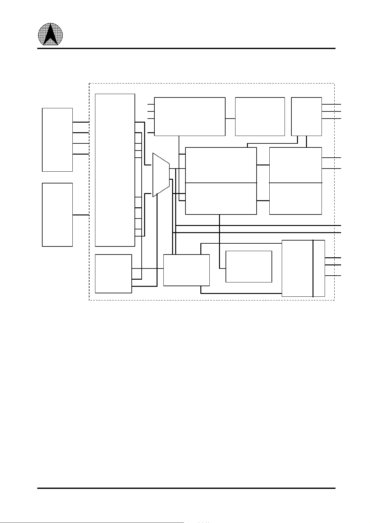
MEM I/F
1.3 Block Diagram
MII
10/100
Q-PHY
I/F
MII
interface
Re-conciliation
Sub-layer
Per port Jabber ctl,
auto-partition SM &
Per port Collision ,
Partition counters.
........
MUX
Registers
Repeater State
Machine of 100Mbps
MIB I/F
(Reserved)
Cascade
Arbitration Logic
of 100Mbps
(Reserved)
10/100
PHY
or
MAC
MII
I/F
(Port 0 Port 4 )
Speed
Detection
circuit
Repeater State
Machine of 10Mbps
Elasticity Buffer
for 100Mbps
and 10Mbps
Fig - 1 Chip Block Diagram
Collision
Handling Logic
for 100Mbps
and10Mbps
(Reserved)
100Mbps
to
10Mbps
Bridge
5
ASIX ELECTRONICS CORPORATION
Page 6

AX88875AP Bripeater
COL[2]
COL[1]
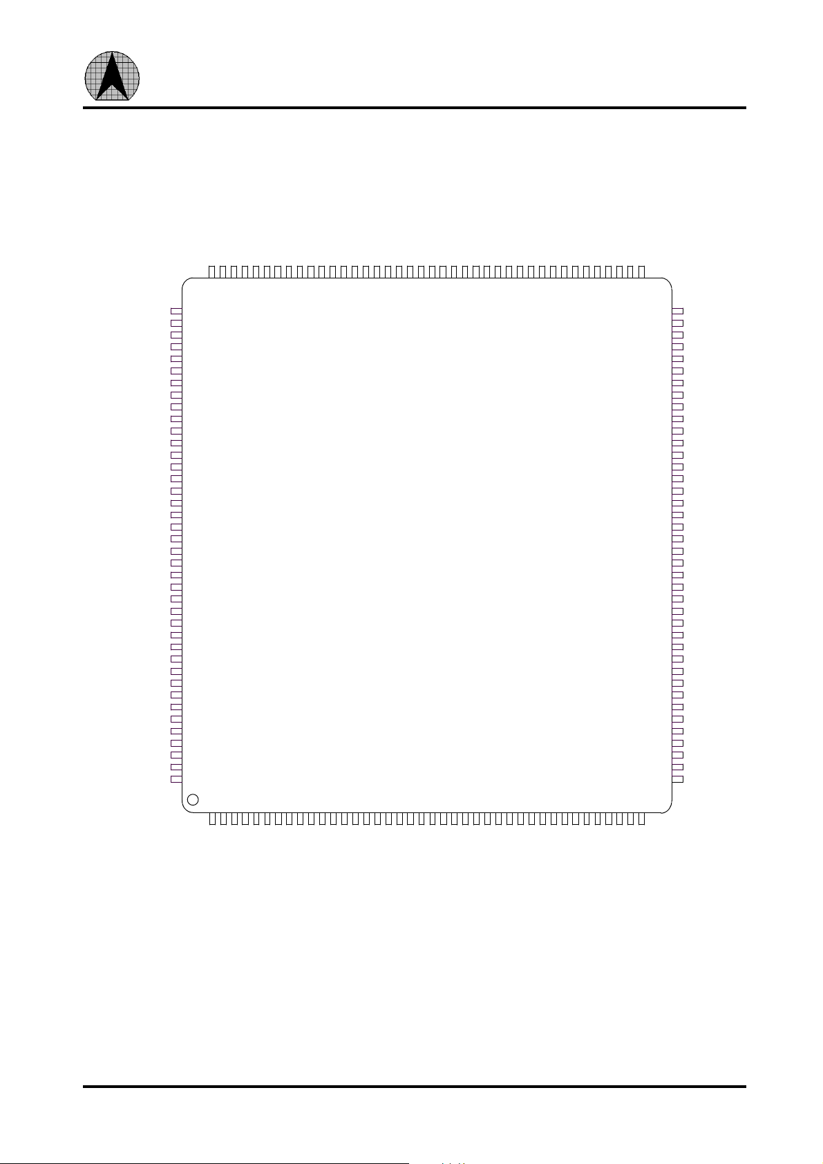
1.4 Pin Connection Diagram (Mode 0)
BMA[6]
BMA[7]
BMA[4]
VSS1
VDD1
109
108
13
12
107
14
106
BMA[5]
105
104
17
16
15
COL[0]
/LACT[4]
NC
/LACT[2]
/LACT[3]
VDD
NC
/LACT[0]
/LACT[1]
NC
TEST1
/RST
VSS
LCLK
/HALF10
VDD
PULL_DN
PULL_DN
VDD1
VSS1
RXER[0]
RXDV[0]
CRS[0]
RXCLK[0]
RXD[0][0]
RXD[0][1]
RXD[0][2]
RXD[0][3]
VSS
TXEN[0]
TXD[0][0]
TXD[0][1]
TXD[0][2]
TXD[0][3]
TXER[0]
RXER[1]
RXDV[1]
CRS[1]
RXCLK[1]
RXD[1][0]
RXD[1][1]
121
122
123
124
125
126
127
128
129
130
131
132
133
134
135
136
137
138
139
140
141
142
143
144
145
146
147
148
149
150
151
152
153
154
155
156
157
158
159
160
/LPART[4]
VSS
/LPART[3]
120
118
117
119
2
3
1
/LUTI[4]
/LPART[2]
/LPART[0]
/TEST2
/LPART[1]
115
116
113
114
4
5
8
6
7
/LCOL10
/LSEL10
/LUTI[5]
110
112
111
AX88875AP
( Mode 0 )
9
11
10
BMA[3]
VDD
102
103
19
18
BMA[2]
BMA[0]
BMA[1]
99
101
100
22
20
21
BMD[7]
VSS
96
97
98
24
23
BMD[4]
BMD[5]
BMD[6]
95
94
25
26
27
BMD[2]
BMD[1]
BMD[3]
93
91
92
29
28
30
BMD[0]
BMA[16]
VSS
88
90
89
31
32
33
BMA[12]
BMA[15]
BMA[14]
BMA[13]
84
86
85
87
35
37
34
36
BMA[10]
BMA[11]
VDD
81
83
82
80
79
78
77
76
75
74
73
72
71
70
69
68
67
66
65
64
63
62
61
60
59
58
57
56
55
54
53
52
51
50
49
48
47
46
45
44
43
42
41
38
39
40
BMA[9]
BMA[8]
/BMWR
/LUTI[3]
/LUTI[2]
/LUTI[1]
/LUTI[0]
/BMA[15]
MCLK
MDO
MDC
/LCOL100
VSS
COL_O[4]
TXER[4]
TXD[4][3]
TXD[4][2]
TXD[4][1]
TXD[4][0]
TXEN[4]
RXD[4][3]
RXD[4][2]
RXD[4][1]
RXD[4][0]
RXCLK[4]
VDD1
VSS1
CRS[4]
RXDV[4]
RXER[4]
VDD
SET2
SET1
SET0
PULL_DN
VSS
TXER[3]
TXD[3][3]
TXD[3][2]
TXD[3][1]
COL[4]
COL[3]
VDD
RXD[1][2]
RXD[1][3]
TXEN[1]
TXD[1][2]
TXD[1][1]
TXD[1][0]
VSS
TXER[1]
PULL_DN
TXD[1][3]
VSS1
VDD1
RXER[2]
PULL_DN
CRS[2]
RXDV[2]
RXD[2][0]
RXCLK[2]
TXEN[2]
RXD[2][1]
RXD[2][2]
RXD[2][3]
TXD[2][1]
TXD[2][0]
VSS
TXER[2]
TXD[2][3]
TXD[2][2]
CRS[3]
RXER[3]
RXDV[3]
RXCLK[3]
Fig - 2 Pin Connection Diagram (Mode 0)
Note : Power on configuration setup signals refer section 2.5 cross referance table
6
ASIX ELECTRONICS CORPORATION
RXD[3][0]
RXD[3][1]
RXD[3][3]
RXD[3][2]
VDD
TXEN[3]
TXD[3][0]
Page 7
AX88875AP Bripeater
COL[2]
COL[1]
1.5 Pin Connection Diagram (Mode 1)
COL[0]
NC
NC
NC
NC
VDD
NC
NC
NC
NC
TEST1
/RST
VSS
LCLK
/HALF10
VDD
PULL_DN
PULL_DN
VDD1
VSS1
RXER[0]
RXDV[0]
CRS[0]
RXCLK[0]
RXD[0][0]
RXD[0][1]
RXD[0][2]
RXD[0][3]
VSS
TXEN[0]
TXD[0][0]
TXD[0][1]
TXD[0][2]
TXD[0][3]
TXER[0]
RXER[1]
RXDV[1]
CRS[1]
RXCLK[1]
RXD[1][0]
RXD[1][1]
121
122
123
124
125
126
127
128
129
130
131
132
133
134
135
136
137
138
139
140
141
142
143
144
145
146
147
148
149
150
151
152
153
154
155
156
157
158
159
160
VSS
120
1
NC
119
2
NC
118
3
NCNCNC
NC
/TEST2
117
115
116
114
4
5
7
6
BMA[1]
BMA[2]
BMA[3]
102
101
BMA[0]
99
100
NC
NC
/LCOL10
111
112
110
113
VSS1
VDD1
109
108
BMA[7]
BMA[5]
BMA[6]
105
107
106
BMA[4]
VDD
103
104
AX88875AP
( Mode 1 )
8
9
12
10
13
11
14
15
16
17
18
19
20
21
VSS
98
22
BMD[6]
BMD[7]
96
97
24
23
BMD[5]
BMD[4]
94
95
26
25
BMD[3]
93
27
28
BMD[2]
BMD[0]
BMD[1]
90
91
92
30
29
31
BMA[15]
BMA[16]
VSS
87
88
89
33
34
32
BMA[12]
BMA[14]
BMA[13]
BMA[11]
83
84
86
85
37
35
36
38
BMA[10]
VDD
81
82
80
79
78
77
76
75
74
73
72
71
70
69
68
67
66
65
64
63
62
61
60
59
58
57
56
55
54
53
52
51
50
49
48
47
46
45
44
43
42
41
40
39
BMA[9]
BMA[8]
/BMWR
LED_CK
LED[2]
LED[1]
LED[0]
/BMA[15]
MCLK
MDO
MDC
/LCOL100
VSS
COL_O[4]
TXER[4]
TXD[4][3]
TXD[4][2]
TXD[4][1]
TXD[4][0]
TXEN[4]
RXD[4][3]
RXD[4][2]
RXD[4][1]
RXD[4][0]
RXCLK[4]
VDD1
VSS1
CRS[4]
RXDV[4]
RXER[4]
VDD
SET2
SET1
SET0
PULL_DN
VSS
TXER[3]
TXD[3][3]
TXD[3][2]
TXD[3][1]
COL[4]
COL[3]
VDD
RXD[1][3]
RXD[1][2]
TXEN[1]
TXD[1][2]
TXD[1][0]
TXD[1][1]
VSS
TXER[1]
TXD[1][3]
PULL_DN
VSS1
VDD1
RXER[2]
PULL_DN
CRS[2]
RXDV[2]
RXCLK[2]
RXD[2][0]
TXEN[2]
RXD[2][3]
RXD[2][2]
RXD[2][1]
TXD[2][1]
TXD[2][0]
VSS
TXER[2]
TXD[2][2]
TXD[2][3]
RXER[3]
RXDV[3]
Fig - 3 Pin Connection Diagram (Mode 1)
Note : Power on configuration setup signals refer section 2.5 cross referance table
7
ASIX ELECTRONICS CORPORATION
CRS[3]
RXCLK[3]
RXD[3][0]
RXD[3][1]
VDD
TXEN[3]
RXD[3][2]
RXD[3][3]
TXD[3][0]
Page 8

AX88875AP Bripeater
2.0 Pin Description
The following terms describe the AX88875A pinout:
All pin names with the “/” suffix are asserted low.
I = Input
O = Output
I/O = Input /Output
2.1 MII interfaces
Signal Name Type Pin No. Description
TXER[4:0]
Or
COL[4:0]
TXD[4:0][3:0] O 65 – 62, 43 – 40
TXEN[4:0] O 61, 39, 23
RXD[4:0][3:0] I 60 – 57, 37 – 34
RXER[4:0] I 51, 30, 15,
RXCLK[4:0] I 56, 33,
RXDV[4:0] I 52, 31,
CRS[4:0] I 53, 32,
COL_O[4] O 67 Collision : Collision detection signal for port 4
O
or
I
66, 44, 28
9, 154
27 – 24, 8 – 5
153 - 150
4, 149
22 – 19, 3, 2
160, 159,
147 - 144
155, 140
18, 158, 143
16, 156, 141
17, 157, 142
Transmit Error : When /HALF10 pin set to “high”. TXER is transition
synchronously with respect to the rising edge of TXCLK . Asserted
high when a code violation is request to be send
Collision : When /HALF10 pin set to “low”. COL is input from PHY,
when 10Mbps PHY is in half-duplex mode.
Transmit Data : TXD[3:0] is transition synchronously with respect to
the rising edge of TXCLK. For each TXCLK period in which TXEN is
asserted, TXD[3:0] are accepted for transmission by the PHY.
Transmit Enable : TXEN is transition synchronously with respect to the
rising edge of TXCLK. TXEN indicates that the port is presenting
nibbles on TXD [3:0] for transmission.
Receive Data : RXD [3:0] is driven by the PHY synchronously with
respect to RXCLK.
Receive Error : RXER ,is driven by PHY and synchronous to RXCLK,
is asserted for one or more RXCLK periods to indicate to the port that
an error has detected.
Receive Clock : RX_CLK is a continuous clock that provides the
timing reference for the transfer of the RXDV,RXD [3:0] and RXER
signals from the PHY to the MII port of the repeater.
Receive Data Valid : RX_DV is driven by the PHY synchronously with
respect to RXCLK. Asserted high when valid data is present on RXD
[3:0].
Carrier Sense : Asynchronous signal CRS is asserted by the PHY when
receive medium is non-idle at full duplex mode.
8
ASIX ELECTRONICS CORPORATION
Page 9

AX88875AP Bripeater
2.2 LED Display
Signal Name Type Pin No. Description
LED[2:0]
or
/LUTI[2:0]
O 76 - 74 LED Display Information : When MODE=”1” , Those signals indicate each
port‘s Partition, Jabber, Activity, Collision (global), Repeater ID, Utilization
% (global), Collision % (global) in sequence. For detail , see the LED timing
specification
/LUTI[2:0] : When MODE=”0” , Those pins drive utilization[2:0] LEDs
directly.
The Utilization % display define as following : (See Note 1 also)
Utilization % LED0 LED1 LED2 LED3 LED4 LED5 LED6 LED7
0 1 1 1 1 1 1 1 1
1 0 1 1 1 1 1 1 1
5 0 0 1 1 1 1 1 1
10 0 0 0 1 1 1 1 1
15 0 0 0 0 1 1 1 1
30 0 0 0 0 0 1 1 1
40 0 0 0 0 0 0 1 1
60 0 0 0 0 0 0 0 1
80+ 0 0 0 0 0 0 0 0
The Collision % display define as following :
Collision % LED0 LED1 LED2 LED3 LED4 LED5 LED6 LED7
0 1 1 1 1 1 1 1 1
1 0 1 1 1 1 1 1 1
2 0 0 1 1 1 1 1 1
5 0 0 0 1 1 1 1 1
10 0 0 0 0 1 1 1 1
15 0 0 0 0 0 1 1 1
20 0 0 0 0 0 0 1 1
30 0 0 0 0 0 0 0 1
60+ 0 0 0 0 0 0 0 0
LED_CK
or
/LUTI[3]
/LCOL10
or
/LUTI[4]
NC
or
/LUTI[5]
/LCOL100 O/Z 69 Collision LED for 100Mbps : This pin indicates 100Mbps repeater collision
NC
or
/LACT[4:0]
NC or
/LPART[4:0]
O 77 LED clock signal : When MODE=”1” , The signal is a discontinue clock for
LED signals serial shift out. The clock period width is 40nS and last 16 cycle
with every 125ms repeated.
/LUTI[3] : When MODE=”0” , This pin drive utilization[3] LED directly.
O/Z 113 Collision LED for 10Mbps : When MODE=”1” , This pin indicates 10Mbps
repeater collision occurred.
/LUTI[4] : When MODE=”0” , This pin drive utilization[4] LED directly.
O 112 NC : When MODE=”1” , The pin function is reserved.
/LUTI[5] : When MODE=”0” , This pin drive utilization[5] LED directly.
occurred.
O 121, 124
123, 128
127
O/OC 119-115 NC : When MODE=”1” , The pin function is reserved. or
NC : When MODE=”1” , The pin function is reserved.
/LACT[4:0] : When MODE=”0” ,Those pins drive activity[4:0] LEDs
directly.
/LPART[4:0] : When MODE=”0” , Those pins drive partition[4:0] LEDs
directly.
9
ASIX ELECTRONICS CORPORATION
Page 10

AX88875AP Bripeater
Note : The Utilization % display define as following for Mode 0 LED direct driving.
Utilization % /LUTI0 /LUTI1 /LUTI2 /LUTI3 /LUTI4 /LUTI5
0 1 1 1 1 1 1
1 0 1 1 1 1 1
5 0 0 1 1 1 1
10 0 0 0 1 1 1
15 0 0 0 0 1 1
30 0 0 0 0 0 1
60 0 0 0 0 0 0
Note 1 :
The calculation formulas of Traffic Utilization between ASIX and NetCom is difference, so you will
get different results when using SmartBit (SB) testing this item.
We found the SmartBit calculate the Utilization without include 96 Bit time inter frame gap. So the
utilization value can be 100%. As well as we found SB used min packet size (64 byte) and min IFG (96
bit-time) as 100% utilization. In theory, when max packet size(1518 byte) and min IFG the utilization
will be more than 100%, but SB also treat it as 100%.
In our AX88875 design, we use real cable bandwidth as calculation base. We calculate the bit counts of
carrier within a unit time. Because of the existence of inter frame gap, In our calculation 100%
utilization is impossible. So the above two cases (64 byte packet size and 1518 byte packet size with
min. IFG ), we will count as 85.7% and 99.2%.
If using SB test result to indicate utilization LED the value must be modified. See the following
reference table.
ASIX’s Utilization% 1 5 10 15 30 60
SmartBit’s Utilization% 2 7 12 17 34 68
2.3 Buffer memory pins group
Signal Name Type Pin No. Description
BMA[16:0] O 88-82,
80, 79,
107-104,
102-99
BMD[7:0] I/O 97-90 Buffer data bus.
/BMWR I/O 78 Memory control pin for write.
/BMA[15] I/O 73 Invert Buffer address 15.
Buffer address bus.
10
ASIX ELECTRONICS CORPORATION
Page 11

AX88875AP Bripeater
2.4 Miscellaneous
Signal Name Type Pin No. Description
LCLK I 133 Local Clock : Must be run at 25Mhz . Used for transmit data to PHY devices,
/RST I 131 Reset : The chip is reset when this signal is asserted Low.
NC
or
/LSEL10
NC
or
/LCOL10
MCLK O 72 MII Clock Out : 2.5MHz 10Mbps MII reference clock
MDO O 71 Station Management Data Out : For setup PHY auto-negotiation registers.
MDC O 70 Station Management Data Clock Out : For MDO reference clock.
TEST1 I/PD 130 Test Pin : The pin is just for test mode setting purpose only. Must be pull low
/TEST2 I/PU 114 Test Pin : The pin is just for test mode setting purpose only. Must be pull high
/HALF10 I/PU 134 Half-duplex mode in 10Mbps : Pull low with 10K ohm resister for 10Mbps
PULL_DN I 11, 12, 46
SET2, SET1,
SET0
VDD I 1, 13, 38
VSS I 10, 14, 29
I/PU 110 NC : No Connection When MODE=”1” .
/LSEL10 : When MODE=”0” , This pin select 10Mbps global LED status
(utilization (%) and collision (%) ) when ‘ low’ ; Otherwise , 100Mbps
LED status is selected.
O/ML 111 NC : No Connection When MODE=” 1”.
/LCOL : When MODE=”0” , This pin drives 10Mbps collision LED directly.
A burst write commands are issue to setup PHY register after reset. The PHY
address 4h, 5h, 6h, 7h, 8h, 9h,Ah and Bh will be written as register 4h to
value 00A1h ( Advertise register set to 10/100 half-duplex mode)and register
0h to value 1000h(Enable auto-negotiation).
when normal operation.
when normal operation.
PHY in half-duplex mode.
Pull Down : Those pins are not use for application. Designer must pull them
136, 137
O 49, 48,47Setup Pins : Those pins are power on configuration use. Default internal pull
50, 55, 81
103, 109
125, 135
138
45, 54, 68
89, 98,
108, 120,
132, 139
148,
down or tie to ground.
high. If necessary, pull low with 10K ohm resister. Tie to ground is
prohibited.
POWER : +5V +/-5%
POWER: 0V
11
ASIX ELECTRONICS CORPORATION
Page 12

AX88875AP Bripeater
2.5 Power on configuration setup signals cross reference table
Signal Name Share with Description
OPT[4] COL_O[4] OPT[4] : Option for external device type to connect to port 4. Default ‘high’ is
for PHY type device. Otherwise, ‘low’ for bridge, switch or MAC type device.
TXM_MODE SET2 TXM_MODE : Option for internal used. Default ‘high’ user may pull the pin
‘low’ with 10K ohm resister for reserve transmition mode alternaty.
MODE SET1
EN_FLOW_CTL SET0 EN_FLOW_CTL = 0 : Disable flow control function.
ST_FW TXD[4][3] ST_FW = 0 : Fragment free forwording mode.
ENTRIES TXD[4][2] ENTRIES = 0 : 1024 entries supported
MEM_SIZE[1]
MEM_SIZE[0]
/IR_ACT_EN /BMWR Inter Repeater Active Input Pin Enable : Designer must keep the pin pull high
TXD[4][1]
TXD[4][0]
All of the above signals are pull-up for default values.
MODE = 0 : Direct LED display mode.
MODE = 1 : Rich LED display mode.
EN_FLOW_CTL = 1 : Enable flow control function.
ST_FW = 1 : Store & forword forwording mode.
ENTRIES = 1 : 256 entries supported
MEM_SIZE[1] MEM_SIZE[0] SIZE (K)
1 1 32K
1 0 64K
0 1 128K
0 0 N/A
to disable the function.
12
ASIX ELECTRONICS CORPORATION
Page 13

AX88875AP Bripeater
3.0 Functional Description
3.1 Repeater State Machine
The repeater state machine is used to control repeater behavior, generates right signal in corresponding
states. The repeater state machine is in Idle state when there is no carrier presented on any ports . When there
is only one port has receive activity, the repeater state machine will enter Data - forwarding State to ensure
correct data forwarding to other connected ports. If collision happens anytime, The repeater state machine
detects collision then send jam pattern to all ports until collision ceases.
idle State
The idle state happens when these conditions exists:
a. /RST is low.
b. All CRS[4:0] are not asserted high in single chip application.
Data Forwarding State
The state happens when the condition exists:
a. Only one signal asserted among CRS[4:0] in single chip application.
The repeater state machine stores receiving packet and transmits to all other ports except for
1. The port is jabbered.
2. The port is isolated.
Collision State
The Collision State happens when these conditions exists:
a. There are two or more signals asserted high among CRS[4:0] in single chip system.
b. Only one carrier exists but RXDV still low exceeds 4 clock cycles in 100BASE-T. The
repeater sends collision pattern to all ports.
One Port Left State
The state happens only when there is no collision but still one port which experienced collision
has receive activity. The repeater remains send collision pattern to all ports except the port.
3.2 RXE /TXE CONTROL
Idle state
The repeater sends no data to any port.
RXE(ALL) = 0.
TXE(ALL) = 0.
Data Forwarding state
If ACTIVE(X) = 1, X is the local connected port,
RXE(X) = 1, RXE(ALL-X) = 0.
TXE(X) = 0, TXE(ALL-X) = 1.
Collision state
The repeater sends jam pattern to all ports.
RXE(ALL) = 0.
TXE(ALL) = 1.
One Port Left state
The repeater sends jam pattern to all other port except for the still activity port.
RXE(ALL) = 0.
TXE(ALL-X) = 1. Suppose X is the one left port.
13
ASIX ELECTRONICS CORPORATION
Page 14

AX88875AP Bripeater
3.3 Jabber State Machine
To prevent an illegally long reception of data from reaching the repeater unit, each port has its own jabber
timer. If a reception exceeds this duration (64K bit times for AX88875A), the jabber condition will be detected.
In this condition, repeater unit will disable receive and transmit packets for the jabbered port and the other ports
remain the normal operation.
When the carrier is no longer detected for the jabbered port or reset the repeater, the jabber function will be
clear and re-enable reception and transmission.
3.4 Partition State Machine
The partition state machine is used to protect network from being upset when a port suffer continuous
collision, each port uses a partition state machine to detect and prevent this condition. When a port suffer from
continuous 64 times of collision events, then it goes to partition state. The partitioned port will be not released
until a packet without collision be transmitted( more than 512 bit times for AX88875A) or reset the repeater.
3.5 LED Display Interface
AX88875A provides per-port LED status indication for partition, jabber, activity and support rate based LED for global partition and collision, utilization (%) for 10/100Mbps. .Detail function is described on
the previous pin description(LED interface). LED[2:0] are all active low. There are two display ways :
complicated and simple way. It depends on the setting of MODE.
Rich LED display application (MODE = 1)
LED[2:0] Status Driver Wave-form as follows :
LED_CK
D0 D1 D2 D3 D4 D5 D6 D7 D8 D9 D11 D12 D13 D14D10 D15
LED[0]
LED[1]
LED[2]
JAB4 JAB3 JAB2 JAB1 JAB0
G
PART
10M
UTI6
RAM
FAIL
10M
UTI5
10M
UTI4
10M
UTI3
10M
UTI2
10M
UTI7
'0'
100M
GCOL
10M
UTI1
10M
GCOL
10M
UTI0
PART
100M
UTI7
PART
100M
UTI3
PART
100M
UTI2
0
1
ACT 0ACT 1ACT 2ACT 3ACT 4
100M
100M
UTI0
UTI1
PART
100M
UTI6
PART
100M
UTI5
2
3
100M
UTI4
4
14
ASIX ELECTRONICS CORPORATION
Page 15

AX88875AP Bripeater
Notes: a. PART4~0indicates partition status for each port b. JAB4~0 indicates jabber status for each port
c. ACT4~0 indicates activity status for each port d. RID2~0 is the ID of repeater chip
e. 10M UTI4~0 indicate global utilization rate of f. 100M UTI4~0 indicate global utilization rate of
10Mbps for each 104.8ms sampling period. 100Mbps for each 104.8ms sampling period.
g. 10M GCOL indicate global collision h. 100M GCOL indicate global collision
i. GPART : indicate global partition. J. RAM FAIL : Bridge RAM test fail.
It must use external shift register to decode data on LED[2:0]. The application shows as follows:
JAB0
PART0
PART1
PART2
PART3
PART4
JAB1
JAB2
JAB3
JAB4
Q
4
3
74LS164(#1)
Q
Q
5
Q
6
7
Q0Q1Q2Q3Q4Q5Q6Q
74LS164(#2)
LED[0]
LED_CK
Q0Q1Q2Q
D D
Fig - 4 Application for LED display
If the user don‘t want to show jabber status, take away the latter 74LS164(#2). The application is the
same for LED[2:1].
Simple LED display application (MODE=0)
LED display for mode 1 vs. mode 0 referance table.
Mode 1 Mode 0 Mode 1 Mode 0 Mode 1 Mode 0
NC /PART[0] NC /ACT[0] LED[0] /UTI[0]
NC /PART[1] NC /ACT[1] LED[1] /UTI[1]
NC /PART[2] NC /ACT[2] LED[2] /UTI[2]
NC /PART[3] NC /ACT[3] LED_CK /UTI[3]
NC /PART[4] NC /ACT[4] NC /UTI[4]
NC /UTI[5]
NC /LCOL10
/LCOL100 /LCOL100
7
15
ASIX ELECTRONICS CORPORATION
Page 16

AX88875AP Bripeater
4.0 INTERNAL REGISTERS
4.1 Configuration Register (CONFIG)
Bit Bit Name Access Bit Description
D9 /HALF10 R/W Half-duplex mode in 10Mbps : “low” resister to 10Mbps PHY in half-
duplex mode. “high” resister to 10Mbps PHY in full-duplex mode.
D8 OPT[4] R/W OPT[4] : Option for external device type to connect to port 4. Default
‘high’ is for PHY type device. Otherwise, ‘low’ for bridge, switch or
MAC type device.
D7 TXM_MODE R/W TXM_MODE : Option for internal used. Default ‘high’ user may pull the
pin ‘low’ with 10K ohm resister for reserve transmition mode alternaty.
D6 MODE R/W
D5 EN_FLOW_
CTL
D4 ST_FW R/W
D3 ENTRIES R/W
D2-1 MEM_SIZE[1]
MEM_SIZE[0]
D0 /IR_ACT_EN R/W Inter Repeater Active Input Pin Enable : Designer must keep the pin pull
MODE = 0 : Single chip repeater application.
MODE = 1 : Multiple chips cascaded repeater application.
R/W EN_FLOW_CTL = 0 : Disable flow control function.
EN_FLOW_CTL = 1 : Enable flow control function.
ST_FW = 0 : fragment-free mode
ST_FW =1 : Store-n-Forward mode
ENTRIES = 0 : 1024 entries supported
ENTRIES = 1 : 256 entries supported
R/W MEM_SIZE[1] MEM_SIZE[1] SIZE (K)
1 1 32K
1 0 64K
0 1 128K
0 0 N/A
high to disable the function.
16
ASIX ELECTRONICS CORPORATION
Page 17

AX88875AP Bripeater
5.0 ELECTRICAL SPECIFICATION AND TIMING
5.1 Absolute Maximum Ratings
Description SYM Min Max Units
Operating Temperature Ta 0 +70
Storage Temperature Ts -55 +150
Supply Voltage Vcc -0.5 +7 V
Input Voltage Vin Vss-0.5 Vdd+0.5 V
Output Voltage Vout Vss-0.5 Vdd+0.5 V
Lead Temperature (soldering 10 seconds maximum) Tl -55 +235
Note : Stress above those listed under Absolute Maximum Ratings may cause permanent damage to the device. Exposure
to Absolute Maximum Ratings conditions for extended period, adversely affect device life and reliability
5.2 General Operation Conditions
Description SYM Min Max Units
Operating Temperature Ta 0 +70
Supply Voltage Vdd +4.75 +5.25 V
°C
°C
°C
°C
5.3 DC Characteristics
(Vdd=4.75V to 5.25V, Vss=0V, Ta=0°C to 70°C)
Description SYM Min Max Units
Low Input Voltage Vil Vss-0.5 0.8 V
High Input Voltage Vih 2 Vdd+0.5 V
Low Output Voltage Vol 0.4 V
High Output Voltage Voh 2.4 V
Input Leakage Current 1 (Note 1) Iil1 10 uA
Input Leakage Current 2 (Note 2) Iil1 500 uA
Output Leakage Current Iol 10 uA
Description SYM Min Tpy Max Units
Power Consumption Pc 120 160 mA
Note :
1. All the input pins without pull low or pull high.
2. Those pins had been pull low or pull high.
17
ASIX ELECTRONICS CORPORATION
Page 18

AX88875AP Bripeater
5.4 AC specifications
5.4.1 MII Interface Timing Tx & Rx
T0 T1
LCLK
T2 T2
TX_EN
T3 T3
TX_ER
TXD
Symbol Description Min Typ. Max Units
T0 Local Clock Cycle Time 39.996 40 40.004 ns
T1 Local Clock High Time 14 20 26 ns
T2 TX_EN Delay from LCLK High 7.440 21.760 ns
T3 TX_ER or TXD Delay from LCLK High 3.410 13.320 ns
T4 T5
RX_CLK
CRS
T6 T7
RXE
T8
RXDV
T9
RXD
RXER
18
ASIX ELECTRONICS CORPORATION
Page 19

AX88875AP Bripeater
T1
T3
T2T4T7T5T6
Symbol Description Min Typ. Max Units
T4 RX_CLK Clock Cycle Time 39.996 40 40.004 ns
T5 RX_CLK Clock High Time 14 20 26 ns
T6 CRS to RXE Assertion Delay 20 ns
T7 CRS to RXE De-assertion Delay 160 200 ns
T8 CRS to RXDV Delay Requirement 40 160 ns
T9 RXD or RXDV or RX_ER setup to RX_CLK rise
time
5.4.2 SRAM read cycle and write cycle
BMA[16:0]
/BMWR
BMD[7:0]
10 - ns
Symbol Description Min Max Units
T1 Read Cycle Time 40 - ns
T2 BMD[7:0] Setup Time 3 - ns
T3 BMD[7:0] Hold Time 3 - ns
BMA[16:0]
/BMWR
BMD[7:0]
Symbol Description Min Max Units
T4 Write Cycle Time 38 - ns
T5 Write Pulse Wtdth 20 - ns
T6 BMD[7:0] Data Valid to End of Write 14 - ns
T7 BMD[7:0] Data Hold from End of Write 1 ns
19
ASIX ELECTRONICS CORPORATION
Page 20

AX88875AP Bripeater
5.4.3 LED DISPLAY
T3
LED_CK
--------
~
~
-------
-
D0 D1 D2 .............. D14 D15
D0 D1 D2
T4
T3
LED_CK
T1
T2
LED[2:0] D0 D1 D2 D3 ------- D15 D0
Symbol Description Min Typ. Max Units
T1 LED setup to LED_CK High 190 200 ns
T2 LED hold from LED_CK High 200 210 ns
T3 LED_CK Period Width 400 ns
T4 continuous 16 LED_CK Cycle Time 52.4 ms
5.4.4 LED Display After Reset
/Reset
T1 T2 T2 T2 T3
LED[2:0]
Symbol Description Min Typ. Max Units
T1 Repeater reset time 1000 ns
T2 LED Blink Time After Reset 838.4 ms
T3 LED Dark Time Before Normal Display 419.2 ms
20
ASIX ELECTRONICS CORPORATION
Page 21

AX88875AP Bripeater
6.0 PACKAGE INFORMATION
Hd
D
pin 1
He
E
b
e
A2 A1
L1
L
θ
MILIMETERSYMBOL
MIN. NOM MAX
A1 0.25
A2 3.15 3.40 3.65
b 0.22 0.30 0.38
D 27.90 28.00 28.10
E 27.90 28.00 28.10
e 0.65
Hd 30.95 31.20 31.45
He 30.95 31.20 31.45
L 0.73 1.03
L1 1.60
θ
0 7°
21
ASIX ELECTRONICS CORPORATION
Page 22

AX88875AP Bripeater
Appendix A: Applications
Two type of applications for AX88875A are illustrated bellow.
A.1 Stand-along 5-ports 10/100Mbps HUB Application
LED Array
AX88875A
Bripeater Controller
MII interface MII interface
Quad
MII
Transceiver
Fig - 5 Stand-along 5-ports 10/100Mbps HUB Application
8 bits
SRAM
Single
MII
Transceiver
A.2 Stand-along 4-ports 10/100Mbps HUB with one MAC Application
LED Array
8 bits
SRAM
AX88875A
Bripeater Controller
MII interface MII interface
Quad
MII
Transceiver
Fig - 6 Stand-along 4-ports 10/100Mbps HUB with one MAC Application
22
AX88195
MAC
ASIX ELECTRONICS CORPORATION
CPU
Page 23

AX88875AP Bripeater
Clock
Appendix B: Using MII I/F connects to MAC
Using MII interface to connect to MAC type device application for AX88875A is illustrated bellow.
25MHz
COL_O4
TXEN4
(LCLK)
TXD4[3:0]
TXER4
CRS4
RXDV4
RXCLK4
RXD4[3:0]
RXER4
10K
Gnd
COL
CRS
RX_DV
RX_CLK
RXD[3:0]
RX_ER
TX_EN
TX_CLK
TXD[3:0]
TX_ER
AX88875 / Repeater AX88195 / MAC
Note : 1. The MAC needs to run at halfduplex mode.
2. Care must be taken that the receive side has enough setup and/or hold time
3. Some kind of CPU with embbeded MAC can also refer to this example
Using MII interface to connect to 10Mbps MAC device application for AX88875A is illustrated bellow.
COL_O4
TXEN4
MCLK
TXD4[3:0]
TXER4
CRS4
RXDV4
RXCLK4
RXD4[3:0]
RXER4
10K
Gnd
COL
CRS
RX_DV
RX_CLK
RXD[3:0]
RX_ER
TX_EN
TX_CLK
TXD[3:0]
TX_ER
AX88875 / Repeater 10Mbps MAC
23
ASIX ELECTRONICS CORPORATION
 Loading...