

Page 1
10/100BASE Dual Speed Repeater Controller
Features
100Mbps horizontal cascade
10Mbps and 100Mbps Vertical cascade upto 4 stacks
10Mbps horizontal cascade
2 Quad RMII PHY
2 Quad RMII PHY
2 Quad RMII PHY
PHY for Up-link
PHY for Down-link or Server
AX88873P
10/100BASE Dual Speed 8-Port Repeater
Ver. 1.1
• IEEE 802.3u repeater compatible
• Supports 8 10/100Mbps RMII I/F repeater ports
• Accompany with AX88872 to build a low cost dual
speed repeater solution
• Up-to 4 repeaters can be cascaded for vertical
expansion
• Up-to 3 chips can be cascaded locally for horizontal
expansion
• All ports can be separately isolated or partitioned in
response to fault condition
• Separate jabber and partition state machines for
each port
• Per-port LED display for Jabber, Partition, Activity
and global collision, utilization (%) for
10/100Mbps presentation
• Power on LED diagnosis. All the LED display will
follow the “ON-OFF-ON-OFF-Normal” operation
procedure during/after power on reset
• 50MHz Operation, 3.3volt and 128-pin PQFP
Product description
The AX88873 10/100Mbps Dual Speed repeater Controller is a counterpart of AX88872 without built in 4-ports
switch. It is design for low cost dual speed dumb HUB application.
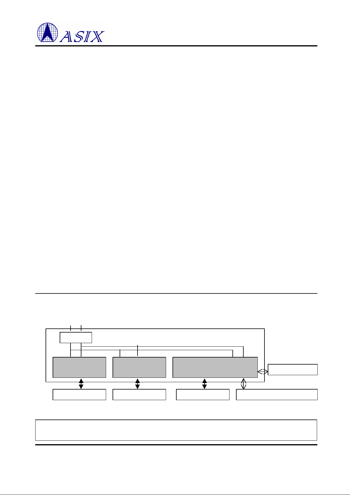
The AX88873 directly supports up-to eight 10/100Mbps automatic links RMII interfaces. Maximum up-to 96
repeater ports can be constructed by stacking 1 AX88872 and 2 AX88873 chips horizontally and then cascading 4
horizontal boards vertically.
With using 128-pin low cost package, accompany with AX88872 to build up low cost dual speed repeater application.
Not only perform the repeater function but gain additional 2 switch ports. The 2 dual speed switch ports are connected
to external MII or RMII interfaces PHY for various applications. For example, one port is use for down link and the
other is used for up link to extend the network topology. The other case is one port for up link and the other port for
server.
The AX88873 is designed base on IEEE 802.3u clause 27 “ Repeater for 100Mb/s base-band networks” It is fully
compatible with IEEE 802.3u standard. Please refer Ax872-11.doc to get more information about AX88872.
System Block Diagram
Buffer
AX88873 #1
Repeater Controller
Always contact ASIX for possible updates before starting a design.
This data sheet contains new products information. ASIX ELECTRONICS reserves the rights to modify product specification without notice. No liability
is assumed as a result of the use of this product. No rights under any patent accompany the sale of the product.
AX88873 #0
Repeater Controller
AX88872 #0
Swipeater Controller
ASIX ELECTRONICS CORPORATION Doc. No. AX873-11.DOC Date : APR/26/1999
2F, NO.13, Industry East Rd. II, Science-based Industrial Park, Hsin-Chu City, Taiwan, R.O.C.
TEL: 886-3-579-9500 FAX: 886-3-579-9558 http://www.asix.com.tw
Page 2

CONFIDENTIAL
AX88873P 10/100Mb Repeater Controller PRELIMINARY
CONTENTS
1.0 AX88873 OVERVIEW....................................................................................................................................... 4
1.1 GENERAL DESCRIPTION...................................................................................................................................... 4
1.2 AX88873 BLOCK DIAGRAM:.............................................................................................................................. 4
1.3 PIN CONNECTION DIAGRAM ............................................................................................................................... 5
2.0 PIN DESCRIPTION........................................................................................................................................... 6
2.1 RMII INTERFACE FOR REPEATER PORTS............................................................................................................... 6
2.1.1 Repeater Port 0 .......................................................................................................................................... 6
2.1.2 Repeater Port 1 .......................................................................................................................................... 6
2.1.3 Repeater Port 2 .......................................................................................................................................... 7
2.1.4 Repeater Port 3 .......................................................................................................................................... 7
2.1.5 Repeater Port 4 .......................................................................................................................................... 7
2.1.6 Repeater Port 5 .......................................................................................................................................... 7
2.1.7 Repeater Port 6 .......................................................................................................................................... 8
2.1.8 Repeater Port 7 .......................................................................................................................................... 8
2.2 EXPANSION BUS INTERFACE FOR 100 MBPS......................................................................................................... 8
2.3 EXPANSION BUS INTERFACE FOR 10 MBPS........................................................................................................... 9
2.4 LED DISPLAY.................................................................................................................................................. 10
2.5 MISCELLANEOUS.............................................................................................................................................. 10
2.6 POWER ON CONFIGURATION SETUP SIGNALS CROSS REFERENCE TABLE ................................................................ 11
3.0 FUNCTIONAL DESCRIPTION..................................................................................................................... 12
3.1 REPEATER STATE MACHINE.............................................................................................................................. 12
3.2 RXE /TXE CONTROL...................................................................................................................................... 12
3.3 JABBER STATE MACHINE.................................................................................................................................. 12
3.4 PARTITION STATE MACHINE............................................................................................................................. 12
3.5 LED DISPLAY INTERFACE................................................................................................................................ 13
4.0 INTERNAL REGISTERS................................................................................................................................ 14
5.0 ELECTRICAL SPECIFICATION AND TIMING.......................................................................................... 15
5.1 ABSOLUTE MAXIMUM RATINGS........................................................................................................................ 15
5.2 GENERAL OPERATION CONDITIONS................................................................................................................... 15
5.3 DC CHARACTERISTICS..................................................................................................................................... 15
5.4 AC SPECIFICATIONS......................................................................................................................................... 16
5.4.1 RMII Interface Timing TX & RX............................................................................................................... 16
5.4.2 MII Interface Timing TX & RX................................................................................................................. 17
5.4.3 LED DISPLAY ......................................................................................................................................... 18
5.4.4 LED Display after Reset........................................................................................................................... 18
6.0 PACKAGE INFORMATION........................................................................................................................... 19
APPENDIX A: APPLICATIONS.......................................................................................................................... 20
A.1 16-PORT (24-PORT) REPEATER WITH 2-PORT SWITCH......................................................................................... 20
A.2 16-PORT REPEATER WITH UPTO 4 STACKS ......................................................................................................... 20
A.3 16-PORT REPEATER WITH UPTO 4 STACKS UP-LINK TO EXTERNAL SWITCH........................................................... 21
2
ASIX ELECTRONICS CORPORATION
Page 3

CONFIDENTIAL
AX88873P 10/100Mb Repeater Controller PRELIMINARY
FIGURES
FIG - 1 AX88873 BLOCK DIAGRAM ............................................................................................................................. 4
FIG - 2 PIN CONNECTION DIAGRAM..............................................................................................................................5
FIG - 3 APPLICATION FOR LED DISPLAY..................................................................................................................... 13
3
ASIX ELECTRONICS CORPORATION
Page 4
CONFIDENTIAL
AX88873P 10/100Mb Repeater Controller PRELIMINARY
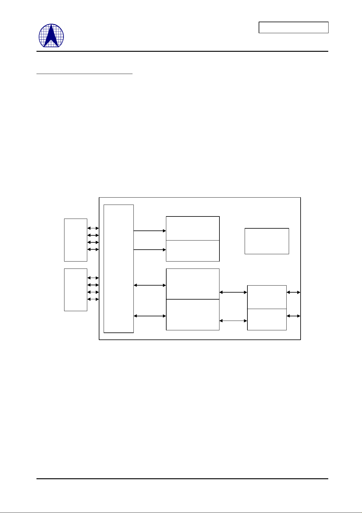
1.0 AX88873 Overview
1.1 General Description
The AX88873 is a simple dual speed repeater that provides two expansion buses for 10M and 100M
segments respectively. Accompany with AX88872 (build-in a 4-port switch) can construct high port
count (16 ports or 24 ports) application and gain 2 additional switch ports. Additional two switch
ports are also useful for up-link or connection of server.
The pin count of chip is reduced to 128 when design uses RMII I/F instead of MII. It is not only
simplify the design but also user can choose low cost RMII Quad PHY.
1.2 AX88873 Block Diagram:
RMII
I/F
10/100
Q-PHY
RMII /MII
translation
for Repeater
Port 0 -7
10/100
Q-PHY
Per Port Jabber
Detection
Per Port Partition
Detection
Repeater State
Machine of 100Mbps
Repeater State
Machine of 10Mbps
Led Interface
Cascade
Arbitration Logic
of 100Mbps
Cascade
Arbitration Logic
of 10Mbps
Fig - 1 AX88873 Block Diagram
4
ASIX ELECTRONICS CORPORATION
Page 5
CONFIDENTIAL
AX88873P 10/100Mb Repeater Controller PRELIMINARY
1.3 Pin Connection Diagram
VSS
TXD5[1]
RXD5[1]
TXD5[0]
TXEN5
CRS_DV5
RXD5[0]
CRS_DV6
RXD6[1]
RXD6[0]
TXD6[0]
TXD6[1]
TXEN6
CRS_DV7
RXD7[1]
RXD7[0]
NC
NC
VDD
SPEED5
SPEED6
SPEED7
VSS
SPEED4
RXD4[1]
TXEN4
TXD4[0]
TXD4[1]
RXD4[0]
CRS_DV4
TXD3[1]
TXD3[0]
TXEN3
RXD3[1]
CRS_DV3
RXD3[0]
VDD
SPEED3
HIRD[2]
HIRD[3]
NC
/HIRD_V
HIRD[0]
HIRD[1]
/HIR_ACTO[3]
HIRD_CK
HIRD_ODIR
VSS
/HIR_ACTI[3]
NC
/HIR_ACTO[0]
/HIR_ACTO[1]
/HIR_ACTO[2]
/HIR_ACTI[2]
VDD
/HIR_ACTI[0]
/HIR_ACTI[1]
/LHIR_ACT[2]
/LHIR_ACT[0]
/LHIR_ACT[1]
VSS
/TIR_ACTI[2]
/TIR_ACTO[1]
/TIR_ACTI[3]
/TIR_ACTO[0]
/TIR_ACTO[2]
/TIR_ACTO[3]
VDD
VSS
/TIR_ACTI[0]
/TIR_ACTI[1]
/LTIR_ACT[1]
/LTIR_ACT[2]
VSS
/LTIR_ACT[0]
TIRD[3]
SPEED0
CRS_DV0
RXD0[0]
RXD0[1]
VDD
TXEN0
TXD0[0]
TXD0[1]
SPEED1
VSS
CRS_DV1
RXD1[0]
RXD1[1]
TXEN1
VSS
TXD1[0]
TXD1[1]
VDD
SPEED2
CRS_DV2
RXD2[0]
RXD2[1]
TXEN2
TXD2[0]
TXD2[1]
VSS
103
104
105
106
107
108
109
110
111
112
113
114
115
116
117
118
119
120
121
122
123
124
125
126
127
128
102
1
101
2
100
3
78
75
77
797480
84
829181
93
94
95
96
989799
90
86
87
8892858983
76
AX88873
8
7
4
6
5
9
10
11
12
13
14
15
16
17
18
19
20
21
22
23
24
25
26
27
28
29
73
30
72
31
71
32
70
33
69
34
68
35
67
36
66
37
65
38
64
63
62
61
60
59
58
57
56
55
54
53
52
51
50
49
48
47
46
45
44
43
42
41
40
39
TIRD[2]
TIRD[1]
TIRD[0]
VSS
/TIRD_V
TIRD_CK
TIRD_ODIR
VDD
LED_CK
LED<1>
LED<0>
VSS
DAISY_OUT
DAISY_IN
VSS
NC
VDD
REF_CLK
VSS
/RST
/TEST
MDO
MDC
TXD7[1]
TXD7[0]
TXEN7
Fig - 2 Pin Connection Diagram
5
ASIX ELECTRONICS CORPORATION
Page 6
CONFIDENTIAL
AX88873P 10/100Mb Repeater Controller PRELIMINARY
2.0 Pin Description
The following terms describe the AX88873 pin out:
All pin names with the “/” suffix are asserted low.
I = Input
O = Output
I/O = Input /Output
2.1 RMII interface for repeater ports
2.1.1 Repeater Port 0
Signal Name Type Pin No. Description
SPEED0 I 103
CRS_DV0 I 104
RXD0[1:0] I 106,105
TXEN0 O 108
TXD0[1:0] O 110,109
Speed Select : SPEED0 is not standard RMII signal. This signal is
sourced from PHY to inform repeater whether 10M or 100M speed is
auto-negociated. Active for 10Mbps speed is selected depending on
power on configuration.
Carrier Sense/Receive Data Valid : CRS_DV is asserted
asynchronously on detection of carrier. CRS_DV is asserted by the PHY
when receive medium is non-idle. Loss of carrier shall result in the
desertion of CRS_DV synchronous to the cycle of REF_CLK, which
presents the first DI-bit of a nibble on to RXD0[1:0].
Receive Data : RXD0[1:0] is synchronous to REF_CLK
RXD0[1:0] shall be “00” to indicate idle when CRS_DV is disserted.
Value other than “00” are reserved for out-of-band signaling shall be
ignored by MAC Upon assertion of CRS_DV, PHY shall ensure that
RXD[1:0] = “00” until proper receive decoding takes place
Transmit Enable : TXEN0 is synchronous to REF_CLK.
TXEN0 indicates that MAC is presenting DI-bits on TXD[1:0] for
transmission. TXEN0 shall be negated prior to the 1st REF_CLK rising
edge following the final DI-bit of a frame
Transmit Data : TXD0[1:0] shall transition synchronously to
REF_CLK. TXD0[1:0] shall be “00” to indicate idle when TX_EN is
disserted. Value other than “00” are reserved for out-of-band signaling
shall be ignored by PHY. When TX_EN is asserted, TXD[1:0] are
accepted for transmission by PHY
2.1.2 Repeater Port 1
Signal Name Type Pin No. Description
SPEED1 I 111
CRS_DV1 I 113
RXD1[1:0] I 115,114
TXEN1 O 116
TXD1[1:0] O 119,118
Speed Select : Please references section 2.1.1 PORT0 description.
Carrier Sense/Receive Data Valid : Please references section 2.1.1
PORT0 description.
Receive Data : Please references section 2.1.1 PORT0 description.
Transmit Enable : Please references section 2.1.1 PORT0 description.
Transmit Data : Please references section 2.1.1 PORT0 description.
6
ASIX ELECTRONICS CORPORATION
Page 7
CONFIDENTIAL
AX88873P 10/100Mb Repeater Controller PRELIMINARY
2.1.3 Repeater Port 2
Signal Name Type Pin No. Description
SPEED2 I 121
Speed Select : Please references section 2.1.1 PORT0 description.
CRS_DV2 I 122
RXD2[1:0] I 124,123 Receive Data : Please references section 2.1.1 PORT0 description.
TXEN2 O 125
TXD2[1:0] O 127,126
Carrier Sense/Receive Data Valid : Please references section 2.1.1
PORT0 description.
Transmit Enable : Please references section 2.1.1 PORT0 description.
Transmit Data : Please references section 2.1.1 PORT0 description.
2.1.4 Repeater Port 3
Signal Name Type Pin No. Description
SPEED3 I 1
CRS_DV3 I 2
RXD3[1:0] I 4,3
TXEN3 O 5
TXD3[1:0] O 7,6
Speed Select : Please references section 2.1.1 PORT0 description.
Carrier Sense/Receive Data Valid : Please references section 2.1.1
PORT0 description.
Receive Data : Please references section 2.1.1 PORT0 description.
Transmit Enable : Please references section 2.1.1 PORT0 description.
Transmit Data : Please references section 2.1.1 PORT0 description.
2.1.5 Repeater Port 4
Signal Name Type Pin No. Description
SPEED4 I 9
CRS_DV4 I 10
RXD4[1:0] I 12,11
TXEN4 O 13
TXD4[1:0] O 15,14
Speed Select : Please references section 2.1.1 PORT0 description.
Carrier Sense/Receive Data Valid : Please references section 2.1.1
PORT0 description.
Receive Data : Please references section 2.1.1 PORT0 description.
Transmit Enable : Please references section 2.1.1 PORT0 description.
Transmit Data : Please references section 2.1.1 PORT0 description.
2.1.6 Repeater Port 5
Signal Name Type Pin No. Description
SPEED5 I 19
CRS_DV5 I 20
RXD5[1:0] I 23,22
TXEN5 O 24
Speed Select : Please references section 2.1.1 PORT0 description.
Carrier Sense/Receive Data Valid : Please references section 2.1.1
PORT0 description.
Receive Data : Please references section 2.1.1 PORT0 description.
Transmit Enable : Please references section 2.1.1 PORT0 description.
TXD5[1:0] O 26,25
Transmit Data : Please references section 2.1.1 PORT0 description.
7
ASIX ELECTRONICS CORPORATION
Page 8

CONFIDENTIAL
AX88873P 10/100Mb Repeater Controller PRELIMINARY
2.1.7 Repeater Port 6
Signal Name Type Pin No. Description
SPEED6 I 27
Speed Select : Please references section 2.1.1 PORT0 description.
CRS_DV6 I 28
RXD6[1:0] I 30,29
TXEN6 O 31
TXD6[1:0] O 33,32
Carrier Sense/Receive Data Valid : Please references section 2.1.1
PORT0 description.
Receive Data : Please references section 2.1.1 PORT0 description.
Transmit Enable : Please references section 2.1.1 PORT0 description.
Transmit Data : Please references section 2.1.1 PORT0 description.
2.1.8 Repeater Port 7
Signal Name Type Pin No. Description
SPEED7 I 35
CRS_DV7 I 36
RXD7[1:0] I 38,37
TXEN7 O 39
TXD7[1:0] O 41,40
Speed Select : Please references section 2.1.1 PORT0 description.
Carrier Sense/Receive Data Valid : Please references section 2.1.1
PORT0 description.
Receive Data : Please references section 2.1.1 PORT0 description.
Transmit Enable : Please references section 2.1.1 PORT0 description.
Transmit Data : Please references section 2.1.1 PORT0 description.
2.2 Expansion Bus Interface for 100 Mbps
Signal Name Type Pin No. Description
HIRD[3:0] I/O/Z
/PU
/HIRD_V I/O/Z
/PU
HIRD_CK I/O/Z
/PU
HIRD_ODIR O 95
/LHIR_ACT[2:0] I/O/OC 83,81,80
/HIR_ACTI[3:0] I/PU 87,86
/HIR_ACTO[3:0] I/O/OC 93,92
101,100
99,98
97
96
85,84
91,90
INTER REPEATER DATA : Nibble data input/output. Transfer data from
the “active” AX88872/3 to all other “inactive” AX88872/3 chips. The busmaster of the IRD bus is determined by IR_ACT bus arbitration.
INTER REPEATER DATA VALID : This signal reflects the RX_DV
status of the active port. Used to frame good packets.
INTER REPEATER CLOCK VALID : All inter repeater signals are
synchronized to the rising edge of this clock.
INTER REPEATER DATA IN/OUT DIRECTION :
This pin indicates the direction of IRD data .
“High” = HIRD[3:0], /HIRD_V , HIRD_CK are Output.
“Low” = HIRD[3:0], /HIRD_V , HIRD_CK are Input.
LOCAL REPEATER ACTIVITY IN/OUT : the function is the same as
/HIR_ACTO[3:0] but for local repeater activity only.
INTER REPEATER ACTIVITY IN: These pins perform the same
function as /HIR_ACTO[3:0] when they serve as input function. Then the
/HIR_ACTO[3:0] insert external buffers the input function must be replaced
with /HIR_ACTI [3:0].
INTER REPEATER ACTIVITY IN/OUT: The local repeater activity
appearance, the signal of the related RID (Repeater ID) will be asserted and
as an output pin. All other pins serve as input pins but except the collision
conditions. When collision occurs , the signal of related (RID-1) pins will
also serve as outputs and will active during local collision period. The
exception case is when RID = 0, then (RID-1) is replaced with (RID+1).
8
ASIX ELECTRONICS CORPORATION
Page 9

CONFIDENTIAL
AX88873P 10/100Mb Repeater Controller PRELIMINARY
2.3 Expansion Bus Interface for 10 Mbps
Signal Name Type Pin No. Description
TIRD[3:0] I/O/Z
/PU
/TIRD_V I/O/Z
/PU
TIRD_CK I/O/Z
/PU
TIRD_ODIR O 58
/LTIR_ACT[2:0] I/O/OC 68,67,66
/TIR_ACTI[3:0] I/PU 74,73,
/TIR_ACTO[3:0] I/O/OC 79,78
65,64
63,62
60
59
72,71
76,75
INTER REPEATER DATA : Nibble data input/output. Transfer data from
the “active” AX88872/3 to all other “inactive” AX88872/3 chips. The busmaster of the IRD bus is determined by IR_ACT bus arbitration.
INTER REPEATER DATA VALID : This signal reflects the RX_DV
status of the active port. Used to frame good packets.
INTER REPEATER CLOCK VALID : All inter repeater signals are
synchronized to the rising edge of this clock.
INTER REPEATER DATA IN/OUT DIRECTION :
This pin indicates the direction of data for external transceiver.
“High” = TIRD[3:0], /TIRD_V , TIRD_CK are Output.
“Low” = TIRD[3:0], /TIRD_V , TIRD_CK are Input.
LOCAL REPEATER ACTIVITY IN/OUT : the function is the same as
/TIR_ACTO[3:0] but for local repeater activity only.
INTER REPEATER ACTIVITY IN: These pins perform the same
function as /HIR_ACTO[3:0] when they serve as input function. Then the
/HIR_ACTO[3:0] insert external buffers the input function must be replaced
with /HIR_ACTI [3:0].
INTER REPEATER ACTIVITY IN/OUT: The local repeater activity
appearance, the signal of the related RID (Repeater ID) will be asserted and
as an output pin. All other pins serve as input pins but except the collision
conditions. When collision occurs , the signal of related (RID-1) pins will
also serve as outputs and will active during local collision period. The
exception case is when RID = 0, then (RID-1) is replaced with (RID+1).
9
ASIX ELECTRONICS CORPORATION
Page 10

CONFIDENTIAL
AX88873P 10/100Mb Repeater Controller PRELIMINARY
2.4 LED Display
Signal Name Type Pin No. Description
LED[1:0] O 55, 54 Those signals indicate each port‘s statuses (such as activity, jabber and
partition) and global information(such as Collision , Repeater ID,
Utilization ) in sequence. For detail , see the LED timing specification
The utilization of 100M segment and 10M segment are using the same scale.
The Utilization % display define as following : (See Note 1 also)
1: Led off
0: Led on
Utilization % UTI0 UTI1 UTI2 UTI3 UTI4 UTI5
0 1 1 1 1 1 1
1 0 1 1 1 1 1
5 0 0 1 1 1 1
10 0 0 0 1 1 1
15 0 0 0 0 1 1
30 0 0 0 0 0 1
60 0 0 0 0 0 0
LED[0] : This signal also indicates 100M repeater collision ( Blinking )
during the interval of sequence shift
data.
LED[1] : This signal also indicates 10 M repeater collision ( Blinking )
during the interval of sequence shift data.
LED_CK O 56
LED Clock : The signal is a discontinue clock for LED signals serial shift
out. The clock period width is 400nS and last 32 cycle with every 52.4ms
repeated.
2.5 Miscellaneous
Signal Name Type Pin No. Description
/RST I 45
REF_CLK I 47
DAISY_IN I/PU 51
DAISY_OUT O/ML 52
MDO O 43
MDC O 42
/TEST I/PD 44
Reset : Active Low
The chip is reset when this signal is asserted Low
Reference clock : The input is a continuous clock at 50Mhz for timing
reference with RMII interface.
Repeater Identification Number Daisy-Chain In : When MODE=”1” ,
This pin is a daisy chain serial input for Repeater ID. A state machine always
monitors the input if a correct data (RID) present at the pin, the (RID+1) will
be written to RID register and override the power on setup RID for the chip.
Repeater Identification Number Daisy-Chain Out : When MODE=”1” ,
This pin is periodically shift out the RID of itself to the next chained chip to
inform that this ID has already been occupied. The RID is shift out
periodically every about 200us.
Station Management Data Out : For setup PHY auto-negotiation registers.
A burst write commands are issue to setup PHY register after reset. The PHY
address 4h, 5h, 6h, 7h, 8h, 9h,Ah and Bh will be written as register 4h to
value 00A1h ( Advertise register set to 10/100 half-duplex mode)and register
0h to value 1000h(Enable auto-negotiation).
Station Management Data Clock Out : For MDO reference clock.
Test Pin : Active LOW
10
ASIX ELECTRONICS CORPORATION
Page 11

CONFIDENTIAL
AX88873P 10/100Mb Repeater Controller PRELIMINARY
The pin is just for test mode setting purpose only. Must be pull high when
normal operation.
NC O 16, 18
49,88
102
VDD I 17, 34
48, 57
77, 89
107, 120
VSS I 8, 21
46, 50
53,61
69, 70
82, 94,
112, 117
NC : Keep no connection
POWER : +3.3V +/-5%
POWER: 0V
128
2.6 Power on configuration setup signals cross reference table
Signal Name Share with Description
Speed_Define TXD7[1]
LRID_S1
LRID_S0
TXD5[1]
TXD5[0]
All of the above signals are pull-up for default values.
Speed Setting for Repeater Port 0 to Port 7 :
0 : SPEED0~7 pin is Low for 10M,high for 100M
1 : SPEED0~7 pin is Low for 100M,high for 10M
Local Repeater ID Selection :
LRID_S1 LRID_S0 LRID No.
1 1 0
1 0 1
0 1 2
0 0 reserved
Note 1 :
The calculation formulae of Traffic Utilization between ASIX and NetCom is difference, so you will get different results
when using SmartBit (SB) testing this item.
We found the SmartBit calculate the Utilization without include 96 Bit time inter frame gap (IFG). So the utilization
value can be 100%. As well as we found SB used min packet size (64 byte) and min IFG (96 bit-time) as 100% utilization.
In theory, when max packet size (1518 byte) and min IFG the utilization will be more than 100%, but SB also treat it as
100%.
In our AX88873 design, we use real cable bandwidth as calculation base. We calculate the bit counts of carrier within a
unit time. Because of the existence of inter frame gap, In our calculation 100% utilization is impossible. So the above two
cases (64 byte packet size and 1518 byte packet size with min. IFG), we will count as 85.7% and 99.2%.
If using SB test result to indicate utilization LED the value must be modified. See the following reference table.
ASIX’s Utilization% 1 5 10 15 30 60
SmartBit’s Utilization% 2 7 12 17 34 68
11
ASIX ELECTRONICS CORPORATION
Page 12

CONFIDENTIAL
AX88873P 10/100Mb Repeater Controller PRELIMINARY
3.0 Functional Description
3.1 Repeater State Machine
The repeater state machine is in idle state when there is no carrier presented on any ports . When there is only
one port has receive activity, the repeater state machine will enter data -forwarding state to ensure correct
data forwarding to other connected ports. If collision happens anytime, The repeater state machine detects
collision then send jam pattern to all ports until collision ceases.
3.2 RXE /TXE Control
Idle state
CRS_DV(ALL) = 0, the repeater sends no data to any port.
RXE(ALL) = 0.
TXE(ALL) = 0.
Data Forwarding state
If CRS_DV(ALL) = 1, N is the only one port that has incoming packet.
RXE(N) = 1, RXE(ALLXN) = 0.
TXE(N) = 0, TXE(ALLXN) = 1.
Collision state
If CRS_DV(ALL) > 1, the repeater sends jam pattern to all ports.
RXE(ALL) = 0.
TXE(ALL) = 1.
One Port Left state
When all packets are back off except only one port still has activity, that is CRS_DV(ALL) = 1 again . N is the
only one left port that has incoming packet. The repeater sends jam pattern to all other port except for the still
activity ports.
RXE(ALL) = 0.
TXE(ALLXN) = 1.
3.3 Jabber State Machine
To prevent an illegally long reception of data from reaching the repeater unit, each port has its own jabber
timer. If a reception exceeds this duration (64K bit times for AX88872A), the jabber condition will be detected.
In this condition, repeater unit will disable receive and transmit packets for the jabbered port and the other ports
remain the normal operation.
When the carrier is no longer detected for the jabbered port or reset the repeater, the jabber state will be existed
and the port will receive and transmit packets normally.
3.4 Partition State Machine
The partition state machine is used to protect network from being upset when a port suffer continuous
collision, each port uses a partition state machine to detect and prevent this condition. When a port suffers from
continuous 64 times of collision events, then it goes to Partition State. The partitioned port will be not released
until a packet without collision be transmitted( more than 512 bit times for AX88872A) or reset the repeater.
12
ASIX ELECTRONICS CORPORATION
Page 13

CONFIDENTIAL
AX88873P 10/100Mb Repeater Controller PRELIMINARY
3.5 LED Display Interface
AX88873 provides per-port LED status indication for partition, jabber, activity and support rate - based LED
for 10 and 100Mbps segments utilization (%) . All LED[1:0] perform active low.
LED[1:0] Status Driver Wave-form as follows :
LED_CK
D0 D1 D2 D3 D4 D5 D6 D7 D8 D9 D11 D12 D13 D14D10 D15
10M
10M
10M
10M
10M
LED[0]
LED[0]
Continue
10M
UTI5
UTI4
UTI3
UTI2
UTI1
UTI0
RID0RID1RID2RID3
UTI5
UTI4
100M
100M
100M
UTI3
100M
UTI2
D16 D19 D20 D21 D22D18 D23D17 ( This portation no clock presented )
ACT0ACT1ACT2ACT3ACT4ACT5ACT6ACT7
Chip 0 Memory Test Fail and/or 100M Collision
100M
UTI1
100M
UTI0
LED[1]
LED[1]
Continue
JAB7 JAB6 JAB5 JAB4 JAB3 JAB2 JAB1 JAB0
PART7PART
6
PART
5
PART
4
PART
3
PART
2
PART
1
PART
0
Chip 1 Memory Test Fail and/or 10M Collision
Notes:
a. PART7~0indicates partition status for each port
b. JAB7~0 indicates jabber status for each port
c. ACT7~0 indicates activity status for each port
d. RID3~0 is the ID of repeater chip
e. 10M UTI5~0 indicate global utilization rate of 10Mbps for each 104.8ms sampling period.
f. 100M UTI5~0 indicate global utilization rate of 100Mbps for each 104.8ms sampling period.
It must use external shift register to decode data on LED[1:0]. The application shows as follows:
RID0
10M UTI0
Q
7
RID1
Q1Q2Q
Q
0
D
100M UTI5
100M UTI4
Q
3
74LS164(#2)
100M UTI3
100M UTI2
Q
4
5
100M UTI0
100M UTI1
Q
Q
7
6
ACT7
Q
0
D
ACT6
ACT5
Q1Q2Q
74LS164(#3)
ACT4
3
LED[0]
LED_CK
RID3
Q
0
D
RID2
10M UTI5
Q1Q2Q
74LS164(#1)
10M UTI4
10M UTI3
Q
4
3
10M UTI2
10M UTI1
Q
Q
5
6
N/AN/AN/AN/AN/AN/AN/AN/A
ACT3
Q
4
ACT2
Q
5
ACT1
Q
6
ACT0
Q
7
Fig - 3 Application for LED display
If the user don‘t want to show jabber status, take away the latter 74LS164(#2). The application is the
same for LED[1].
13
ASIX ELECTRONICS CORPORATION
Page 14

CONFIDENTIAL
AX88873P 10/100Mb Repeater Controller PRELIMINARY
4.0 INTERNAL REGISTERS
The information reserve for intelligent function.
14
ASIX ELECTRONICS CORPORATION
Page 15

CONFIDENTIAL
AX88873P 10/100Mb Repeater Controller PRELIMINARY
5.0 ELECTRICAL SPECIFICATION AND TIMING
5.1 Absolute Maximum Ratings
Description SYM Min Max Units
Operating Temperature Ta 0 +70
Storage Temperature Ts -55 +150
Supply Voltage Vcc -0.3 +4 V
Input Voltage Vin -0.3 Vdd+0.5 V
Output Voltage Vout -0.3 Vdd+0.5 V
Lead Temperature (soldering 10 seconds maximum) Tl -55 +220
Note : Stress above those listed under Absolute Maximum Ratings may cause permanent damage to the device. Exposure
to Absolute Maximum Ratings conditions for extended period, adversely affect device life and reliability
5.2 General Operation Conditions
Description SYM Min Max Units
Operating Temperature Ta 0 +70
Supply Voltage Vdd +3.0 +3.6 V
5.3 DC Characteristics
(Vdd=3.0V to 3.6V, Vss=0V, Ta=0°C to 70°C)
Description SYM Min Max Units
Low Input Voltage Vil Vss-0.3 0.8 V
High Input Voltage Vih 2 Vdd+0.5 V
Low Output Voltage Vol 0.4 V
High Output Voltage Voh 2.4 V
Input Leakage Current 1 (Note 1) Iil1 10 uA
Input Leakage Current 2 (Note 2) Iil1 500 uA
Output Leakage Current Iol 10 uA
°C
°C
°C
°C
Description SYM Min Tpy Max Units
Power Consumption Pc TBD mA
Note :
1. All the input pins without pull low or pull high.
2. Those pins had been pull low or pull high.
15
ASIX ELECTRONICS CORPORATION
Page 16

CONFIDENTIAL
AX88873P 10/100Mb Repeater Controller PRELIMINARY
5.4 AC specifications
5.4.1 RMII Interface Timing TX & RX
T0 T1
REF_CLK
T2 T3
TX_EN
TXD
CRS_DV
T2 T3
RXD
Symbol Description Min Typ. Max Units
T0 REF_CLK Clock Cycle Time 19.998 20 20.002 ns
T1 REF_CLK Clock High Time 7 10 13 ns
T2 CRS_DV, RXD, TXEN and TXD data setup to
REF_CLK rising edge
T3 CRS_DV, RXD, TXEN and TXD data hold from
REF_CLK rising edge
4 ns
2 ns
16
ASIX ELECTRONICS CORPORATION
Page 17

CONFIDENTIAL
AX88873P 10/100Mb Repeater Controller PRELIMINARY
5.4.2 MII Interface Timing TX & RX
T0 T1
TXCLK
T2 T2
TX_EN
T3 T3
TXD
Symbol Description Min Typ. Max Units
T0 TXCLK Cycle Time 39.996 40 40.004 ns
T1 TXCLK High Time 14 20 26 ns
T2 TX_EN Delay from TXCLK High 7.440 21.760 ns
T3 TXD Delay from TXCLK High 3.410 13.320 ns
T4 T5
RX_CLK
CRS
T6
RXDV
T7
RXD
Symbol Description Min Typ. Max Units
T4 RX_CLK Clock Cycle Time 39.996 40 40.004 ns
T5 RX_CLK Clock High Time 14 20 26 ns
T6 CRS to RXDV Delay Requirement 40 160 ns
T7 RXD or RXDV setup to RX_CLK rise time 10 - ns
17
ASIX ELECTRONICS CORPORATION
Page 18

CONFIDENTIAL
AX88873P 10/100Mb Repeater Controller PRELIMINARY
5.4.3 LED DISPLAY
T3
LED_CK
--------
~
~
-------
-
D0 D1 D2 .............. D22 D23
D0 D1 D2
T4
T3
LED_CK
T1
T2
LED[1:0] D0 D1 D2 D3 ------- D15 D0
Symbol Description Min Typ. Max Units
T1 LED setup to LED_CK High 190 200 ns
T2 LED hold from LED_CK High 200 210 ns
T3 LED_CK Period Width 400 ns
T4 LED_CK Cycle burst out period 52.4 ms
5.4.4 LED Display after Reset
/Reset
T1 T2 T2 T2 T3
LED[2:0]
Symbol Description Min Typ. Max Units
T1 Repeater reset time 1000 ns
T2 LED Blink Time After Reset 838.4 ms
T3 LED Dark Time Before Normal Display 419.2 ms
18
ASIX ELECTRONICS CORPORATION
Page 19

CONFIDENTIAL
AX88873P 10/100Mb Repeater Controller PRELIMINARY
6.0 Package Information
Hd
D
pin 1
He
E
b
e
A2 A1
L1
L
θ
MILIMETERSYMBOL
MIN. NOM MAX
A1 0.21 0.31 0.41
A2 2.80 2.85 2.90
b 0.15 0.20 0.30
D 13.80 14.00 14.20
E 19.80 20.00 20.20
e 0.50
Hd 17.10 17.20 17.30
He 23.10 23.20 23.30
L 0.70 0.80 0.90
L1 1.60
θ
0 8
19
ASIX ELECTRONICS CORPORATION
Page 20

CONFIDENTIAL
AX88873P 10/100Mb Repeater Controller PRELIMINARY
Appendix A: Applications
100Mbps horizontal cascade
10Mbps and 100Mbps Vertical cascade upto 4 stacks
10Mbps horizontal cascade
2 Quad RMII PHY
2 Quad RMII PHY
PHY for Up-link
PHY for Down-link or Server
100Mbps horizontal cascade
10Mbps and 100Mbps Vertical cascade upto 4 stacks
10Mbps horizontal cascade
2 Quad RMII PHY
2 Quad RMII PHY
PHY for Up-link
PHY for Down-link or Server
100Mbps horizontal cascade
10Mbps horizontal cascade
2 Quad RMII PHY
2 Quad RMII PHY
PHY for Up-link
PHY for Down-link or Server
Some typical applications for AX88873 are illustrated bellow.
A.1 16-port (24-port) repeater with 2-port switch
Buffer
AX88873 #1
Repeater Controller
Note : Add additional AX88873 to build a 24-port repeater
A.2 16-port repeater with upto 4 stacks
Buffer
AX88873 #1
Repeater Controller
AX88872 #0
Swipeater Controller
Repeater #3
Slave
AX88872 #0
Swipeater Controller
Buffer
AX88873 #1
Repeater Controller
20
AX88872 #0
Swipeater Controller
ASIX ELECTRONICS CORPORATION
Repeater #1,#2
Slave (omitted)
Repeater #0
Master
Page 21

CONFIDENTIAL
AX88873P 10/100Mb Repeater Controller PRELIMINARY
A.3 16-port repeater with upto 4 stacks up-link to external switch
10Mbps and 100Mbps horizontal cascade
10Mbps and 100Mbps Vertical cascade upto 4 stacks
10Mbps and 100Mbps horizontal
2 Quad RMII PHY
2 Quad RMII PHY
Quad PHY
Quad PHY or Single PHY
10M Link
100M
Buffer
AX88873 #1
Repeater Controller
2 Quad RMII PHY 2 Quad RMII PHY
Buffer
AX88873 #1
Repeater Controller
AX88873 #0
Repeater Controller
AX88873 #0
Repeater Controller
AX88620
8-port Switch Controller
or
AX88615
5-port Switch Controller
21
ASIX ELECTRONICS CORPORATION
 Loading...