

Page 1

AX88790 L
3-in-1 PCMCIA Fast Ethernet Controller
DAA
MAGNETIC
PCMCIA I/F
EEPROM
MAGNETIC
RJ11
10/100BASE 3-in-1 PCMCIA Fast Ethernet Controller
Document No.: AX790-15 / V1.5 / Jan. 24 ’02
Features
• Highly integrated with embedded 10/100Mbps
MAC, PHY and Transceiver
• Compliant with IEEE 802.3/802.3u
100BASE-TX/FX specification
• Single chip PCMCIA bus 10/100Mbps Fast
Ethernet MAC Controller
• Embedded 8K * 16 bit SRAM
• NE2000 register level compatible instruction
• Compliant with 16 bit PC Card Standard -
February 1995
• Support both 10Mbps and 100Mbps data rate
• Support both full-duplex or half-duplex operation
• Provides FAX/MODEM interface for COMBO AP
• Provides an extra MII port for supporting other
media. For example, Home-LAN application
Product description
The AX88790 Fast Ethernet Controller is a high performance and highly integrated PCMCIA bus Ethernet Controller
with embedded 10/100Mbps PHY/Transceiver and 8K*16 bit SRAM. The AX88790 contains a 16 bit PCMCIA
interfaces to host CPU and compliant with PC Card Standard – February 1995. The AX88790 implements both 10Mbps
and 100Mbps Ethernet function based on IEEE802.3 / IEEE802.3u LAN standard. The AX88790 also provides an extra
IEEE802.3u compliant media-independent interface (MII) to support other media applications. Using MII interface,
Home LAN PHY type media can be supported. The AX88790 is built in interface to connect FAX/MODEM chipset with
parallel bus interface.
Typical System Block Diagram
RJ11
MODEM
AX88790 with 10/100 PHY/TxRx
RJ45
• Support 128/256 bytes EEPROM (used for saving
CIS)
• Support automatic loading of Ethernet ID, CIS and
Adapter Configuration from EEPROM on
power-on initialization
• External and internal loop-back capability
• Support 3 General Purpose Input pins
• Low Power Consumption, typical under 100mA
• 128-pin LQFP low profile package
• 0.25 Micron low power CMOS process. 25MHz
Operation, Pure 3.3V operation with 5V I/O
tolerance.
*IEEE is a registered trademark of the Institute of Electrical and Electronic
Engineers, Inc.
*All other trademarks and registered trademark are the property of their
respective holders.
Home LAN PHY
/TxRx
This data sheet contains new products information. ASIX ELECTRONICS reserves the rights to modify product specification without notice. No liability
Always contact ASIX for possible updates before starting a design.
is assumed as a result of the use of this product. No rights under any patent accompany the sale of the product.
ASIX ELECTRONICS CORPORATION Frist Released Date : Jun/19/2000
2F, NO.13, Industry East Rd. II, Science-based Industrial Park, Hsin-Chu City, Taiwan, R.O.C.
TEL: 886-3-579-9500 FAX: 886-3-579-9558 http://www.asix.com.tw
Page 2

AX88790 L 3-in-1 PCMCIA Fast Ethernet Controller
CONTENTS
1.0 INTRODUCTION .............................................................................................................................................. 5
1.1 GENERAL DESCRIPTION:..................................................................................................................................... 5
1.2 AX88790 BLOCK DIAGRAM:.............................................................................................................................. 5
1.3 AX88790 PIN CONNECTION DIAGRAM ............................................................................................................... 6
2.0 SIGNAL DESCRIPTION................................................................................................................................... 7
2.1 PCMCIA BUS INTERFACE SIGNALS GROUP......................................................................................................... 7
2.2 EEPROM SIGNALS GROUP ................................................................................................................................8
2.3 MII INTERFACE SIGNALS GROUP.......................................................................................................................... 8
2.4 10/100MBPS TWISTED-PAIR INTERFACE PINS GROUP ........................................................................................... 9
2.5 BUILT-IN PHY LED INDICATOR PINS GROUP ....................................................................................................... 9
2.6 MODEM INTERFACE PINS GROUP.......................................................................................................................... 9
2.7 GENERAL PURPOSE I/O PINS GROUP .................................................................................................................. 10
2.8 MISCELLANEOUS PINS GROUP............................................................................................................................ 11
2.9 POWER ON CONFIGURATION SETUP SIGNALS CROSS REFERENCE TABLE ................................................................ 12
3.0 MEMORY AND I/O MAPPING...................................................................................................................... 13
3.1 EEPROM MEMORY MAPPING.......................................................................................................................... 13
3.2 ATTRIBUTE MEMORY MAPPING........................................................................................................................ 13
3.3 I/O MAPPING................................................................................................................................................... 14
3.4 SRAM MEMORY MAPPING .............................................................................................................................. 14
4.0 REGISTERS OPERATION............................................................................................................................. 15
4.1 PCMCIA FUNCTION CONFIGURATION REGISTER SET OF LAN........................................................................... 15
4.1.1 Configuration Option Register of LAN (LCOR) Offset 3C0H (Read/Write)............................................... 16
4.1.2 Configuration and Status Register of LAN (LCSR) Offset 3C2H (Read/Write) ......................................... 17
4.1.3 I/O Base Register 0/1 of LAN (LIOBASE0/1) Offset 3CAH/3CCH (Read/Write) ...................................... 17
4.2 PCMCIA FUNCTION CONFIGURATION REGISTER SET OF MODEM.................................................................... 18
4.2.1 Configuration Option Register of MODEM (MCOR) Offset 3E0H (Read/Write)...................................... 18
4.2.2 Configuration and Status Register of MODEM (MCSR) Offset 3E2H (Read/Write) ................................. 19
4.2.3 I/O Base Register 0/1 of MODEM (MIOBASE0/1) Offset 3EAH/3ECH (Read/Write) .............................. 19
4.3 MAC CORE REGISTERS.................................................................................................................................... 20
4.3.1 Command Register (CR) Offset 00H (Read/Write)................................................................................... 22
4.3.2 Interrupt Status Register (ISR) Offset 07H (Read/Write).......................................................................... 22
4.3.3 Interrupt mask register (IMR) Offset 0FH (Write).................................................................................... 23
4.3.4 Data Configuration Register (DCR) Offset 0EH (Write).......................................................................... 23
4.3.5 Transmit Configuration Register (TCR) Offset 0DH (Write) .................................................................... 23
4.3.6 Transmit Status Register (TSR) Offset 04H (Read)................................................................................... 24
4.3.7 Receive Configuration (RCR) Offset 0CH (Write).................................................................................... 24
4.3.8 Receive Status Register (RSR) Offset 0CH (Read) ................................................................................... 24
4.3.9 Inter-frame gap (IFG) Offset 16H (Read/Write) ....................................................................................... 24
4.3.10 Inter-frame gap Segment 1(IFGS1) Offset 12H (Read/Write)................................................................. 25
4.3.11 Inter-frame gap Segment 2(IFGS2) Offset 13H (Read/Write)................................................................. 25
4.3.12 MII/EEPROM Management Register (MEMR) Offset 14H (Read/Write)................................................. 25
4.3.13 Test Register (TR) Offset 15H (Write).................................................................................................... 25
4.3.14 Test Register (TR) Offset 15H (Read) .................................................................................................... 25
4.3.15 General Purpose Input Register (GPI) Offset 17H (Read)...................................................................... 26
4.3.16 GPO and Control (GPOC) Offset 17H (Write)....................................................................................... 26
4.4 THE EMBEDDED PHY REGISTERS..................................................................................................................... 27
4.4.1 MR0 -- Control Register Bit Descriptions................................................................................................. 28
4.4.2 MR1 -- Status Register Bit Descriptions................................................................................................... 29
4.4.3 MR2, MR3 -- Identification Registers (1 and 2) Bit Descriptions .............................................................. 30
4.4.4 MR4 – Autonegotiation Advertisement Registers Bit Descriptions ............................................................ 30
4.4.5 MR5 – Autonegotiation Link Partner Ability (Base Page) Register Bit Descriptions................................. 30
2
ASIX ELECTRONICS CORPORATION
Page 3

AX88790 L 3-in-1 PCMCIA Fast Ethernet Controller
4.4.6 MR5 –Autonegotiation Link Partner (LP) Ability Register (Next Page) Bit Descriptions .......................... 31
4.4.7 MR6 – Autonegotiation Expansion Register Bit Descriptions................................................................... 31
4.4.8 MR7 –Next Page Transmit Register Bit Descriptions ............................................................................... 32
4.4.9 MR16 – PCS Control Register Bit Descriptions........................................................................................ 32
4.4.10 MR17 –Autonegotiation Register A Bit Descriptions.............................................................................. 33
4.4.11 MR18 –Autonegotiation Register B Bit Descriptions.............................................................................. 33
4.4.12 MR20 –User Defined Register Bit Descriptions...................................................................................... 33
4.4.13 MR21 –RXER Counter Register Bit Descriptions ................................................................................... 34
4.4.14 MR28 –Device-Specific Register 1 (Status Register) Bit Descriptions..................................................... 34
4.4.15 MR29 –Device-Specific Register 2 (100Mbps Control) Bit Descriptions................................................. 35
4.4.16 MR30 –Device-Specific Register 3 (10Mbps Control) Bit Descriptions................................................... 36
4.4.17 MR31 –Device-Specific Register 4 (Quick Status) Bit Descriptions........................................................ 37
5.0 DEVICE ACCESS FUNCTIONS.................................................................................................................... 38
5.1 PCMCIA INTERFACE ACCESS FUNCTIONS.......................................................................................................... 38
5.1.1 Attribute Memory access function functions............................................................................................. 38
5.1.1 I/O access function functions.................................................................................................................... 38
5.2 MII STATION MANAGEMENT FUNCTIONS.......................................................................................................... 39
6.0 ELECTRICAL SPECIFICATION AND TIMINGS....................................................................................... 40
6.1 ABSOLUTE MAXIMUM RATINGS........................................................................................................................ 40
6.2 GENERAL OPERATION CONDITIONS................................................................................................................... 40
6.3 DC CHARACTERISTICS..................................................................................................................................... 40
6.4 A.C. TIMING CHARACTERISTICS....................................................................................................................... 41
6.4.1 XTAL / CLOCK........................................................................................................................................ 41
6.4.2 Reset Timing............................................................................................................................................ 41
6.4.3 Attribute Memory Read Timing................................................................................................................ 43
6.4.4 Attribute Memory Write Timing................................................................................................................ 44
6.4.5 I/O Read Timing....................................................................................................................................... 45
6.4.6 I/O Write Timing...................................................................................................................................... 46
6.4.7 MII Timing ............................................................................................................................................... 47
7.0 PACKAGE INFORMATION........................................................................................................................... 48
APPENDIX A: APPLICATION NOTE 1............................................................................................................. 49
A.1 USING CRYSTAL 25MHZ ................................................................................................................................. 49
A.2 USING OSCILLATOR 25MHZ ............................................................................................................................ 49
APPENDIX B: POWER CONSUMPTION REFERENCE DATA...................................................................... 50
ERRATA OF AX88790 .......................................................................................................................................... 51
DEMONSTRATION CIRCUIT (A) : AX88790 + HOMEPNA 1M8 PHY.......................................................... 52
DEMONSTRATION CIRCUIT (B) : AX88790 ONLY....................................................................................... 57
3
ASIX ELECTRONICS CORPORATION
Page 4

AX88790 L 3-in-1 PCMCIA Fast Ethernet Controller
FIGURES
FIG - 1 AX88790 BLOCK DIAGRAM ............................................................................................................................. 5
FIG - 2 AX88790 PIN CONNECTION DIAGRAM.............................................................................................................. 6
TABLES
TAB - 1 PCMCIA BUS INTERFACE SIGNALS GROUP........................................................................................................ 7
TAB - 2 EEPROM BUS INTERFACE SIGNALS GROUP....................................................................................................... 8
TAB - 3 MII INTERFACE SIGNALS GROUP....................................................................................................................... 8
TAB - 4 10/100MBPS TWISTED-PAIR INTERFACE PINS GROUP......................................................................................... 9
TAB - 5 BUILT-IN PHY LED INDICATOR PINS GROUP .................................................................................................... 9
TAB - 6 MODEM INTERFACE SIGNALS GROUP............................................................................................................... 10
TAB – 7 GENERAL PURPOSES I/O PINS GROUP ............................................................................................................. 10
TAB – 8 MISCELLANEOUS PINS GROUP ........................................................................................................................ 11
TAB - 9 POWER ON CONFIGURATION SETUP TABLE ..................................................................................................... 12
TAB – 10 EEPROM MEMORY MAPPING .................................................................................................................... 13
TAB – 11 ATTRIBUTE MEMORY MAPPING................................................................................................................... 13
TAB – 12 I/O ADDRESS MAPPING............................................................................................................................... 14
TAB – 13 LOCAL MEMORY MAPPING.......................................................................................................................... 14
TAB – 14 PCMCIA FUNCTION CONFIGURATION REGISTER MAPPING OF LAN ............................................................. 15
TAB – 15 PCMCIA FUNCTION CONFIGURATION REGISTER MAPPING OF MODEM ...................................................... 18
TAB - 16 PAGE 0 OF MAC CORE REGISTERS MAPPING................................................................................................ 20
TAB - 17 PAGE 1 OF MAC CORE REGISTERS MAPPING................................................................................................ 21
TAB – 18 THE EMBEDDED PHY REGISTERS................................................................................................................ 27
TAB - 19 MII MANAGEMENT FRAME FORMAT ............................................................................................................ 39
TAB - 20 MII MANAGEMENT FRAMES- FIELD DESCRIPTION......................................................................................... 39
4
ASIX ELECTRONICS CORPORATION
Page 5

AX88790 L 3-in-1 PCMCIA Fast Ethernet Controller
Registers
LOADER I/F
SD[15:0]
SA[9:0]
Ctl BUS
MII I/F
SMDIO
EEDO
TPI, TPO
1.0 Introduction
1.1 General Description:
The AX88790 provides industrial standard NE2000 registers level compatible instruction set. Various drivers are easy
acquired, maintenance and usage with no pain and tears
The AX88790 Fast Ethernet Controller is a high performance and highly integrated PCMCIA bus Ethernet Controller
with embedded 10/100Mbps PHY/Transceiver and 8K*16 bit SRAM. The AX88790 contains a 16 bit PCMCIA
interfaces to host CPU and compliant with PC Card Standard – February 1995. The AX88790 implements both 10Mbps
and 100Mbps Ethernet function based on IEEE802.3 / IEEE802.3u LAN standard. The AX88790 also provides an extra
IEEE802.3u compliant media-independent interface (MII) to support other media applications. Using MII interface,
Home LAN PHY type media can be supported. The AX88790 is also built in interface to connect FAX/MODEM chipset
with parallel bus interface.
The main difference between AX88790 and AX88190 are: 1) Embedded packet buffer memory 2) Built-in 10/100Mbps
PHY/Transceiver 3) Replace memory I/F with PHY/Transceiver I/F. 4) Fix OE# signal synchronous problem 5) Fix
interrupt status can’t always clean up problem of AX88190. 6) Add 3 general-purpose input pins.
AX88790 use 128-pin LQFP low profile package, 25MHz operation, and single 3.3V operation with 5V I/O tolerance.
The ultra low power consumption is an outstanding feature and enlarges the application field. It is suitable for some
power consumption sensitive product like Compact Flash Adapter Card, PDA (Personal Digital Assistant) and Palm size
computer …etc.
1.2 AX88790 Block Diagram:
Fig - 1 AX88790 Block Diagram
EECS
EECK
EEDI
GPI
MODEM
I/F
SEEPROM
NE2000/GPI
and Memory Arbiter
8K* 16 SRAM
Remote
DMA
FIFOs
PCMCIA Interface
SMDC
STA
MAC
Core
&
PHY
5
ASIX ELECTRONICS CORPORATION
Page 6

AX88790 L 3-in-1 PCMCIA Fast Ethernet Controller
INPACK#
1.3 AX88790 Pin Connection Diagram
The AX88790 is housed in the 128-pin plastic light quad flat pack. See Fig - 2 AX88790 Pin
Connection Diagram.
GPI[0]/LINK
VDD
VSS
GPI[1]/DPX
TX_CLK
TX_EN
TXD[0]
TXD[1]
TXD[2]
TXD[3]
GPI[2]/SPD
VDD
VSS
MDCS#
MINT
MAUDIO
MRIN#
MPWDN
MRESET#
MRDY
IOIS16#
STSCHG#
SPKR#
VDD
VSS
REG#
103
104
105
106
107
108
109
110
111
112
113
114
115
116
117
118
119
120
121
122
123
124
125
126
127
128
COL
RX_DV
CRS
100
101
102
3
1
2
RESET
WAIT#
RXD[3]
RXD[2]
RXD[1]
RX_CLK
96
989799
7
4
6
5
SA[1]
SA[0]
SA[3]
SA[2]
VSSM
RXD[0]
VSS
93
94
95
8
9
10
SA[5]
SA[4]
SA[6]
TPOP
VSSO
TPON
VSSO
REXT10
VSSO
VDDO
ZVREG
90
VSSA
REXT100
86
84
87
8892858983
AX88790
12
11
SA[7]
SA[8]
13
14
VSS
VDD
16
15
SA[9]
IREQ#
17
18
WE#
IOWR#
19
20
OE#
IORD#
LCLK/XTALIN
XTALOUT
VSSPD
VDDA
797480
829181
24
21
23
22
CE2#
CE1#
SD[15]
SD[14]
VDDPD
VSSM
VDDM
78
77
76
26
25
27
VDD
SD[13]
SD[12]
VDDA
REXTBS
VSSA
75
73
28
29
30
VSS
SD[11]
SD[10]
TPIN
VSSA
71
72
32
31
SD[9]
SD[8]
TPIP
VDDA
70
69
33
34
VSS
SD[7]
MDC
VSSA
68
67
36
35
SD[6]
SD[5]
TEST1
MDIO
66
65
38
37
SD[3]
SD[4]
64
63
62
61
60
59
58
57
56
55
54
53
52
51
50
49
48
47
46
45
44
43
42
41
40
39
VSS
VSS
I_ACT
I_SPEED
I_LINK
FAST_MODE#
EEPROM_SIZE
VDD
VDDA
VSSA
VSS
VDD
VSS
EECS
EECK
EEDI
EEDO
TEST2
IDDQ
BIST
CLKO25M
VSS
SD[0]
SD[1]
VDD
SD[2]
Fig - 2 AX88790 Pin Connection Diagram
6
ASIX ELECTRONICS CORPORATION
Page 7

AX88790 L 3-in-1 PCMCIA Fast Ethernet Controller
directional data
IREQ# is asserted to indicate the host system that
This signal is set low to insert wait states during Remote DMA
The OE# line is used to gate Memory Read data from
nd
The signal is asserted when the AX88790 is
2.0 Signal Description
The following terms describe the AX88790 pin-out:
All pin names with the “#” suffix are asserted low.
The following abbreviations are used in following Tables.
I Input PU Pull Up
O Output PD Pull Down
I/O Input/Output P Power Pin
OD Open Drain
2.1 PCMCIA Bus Interface Signals Group
SIGNAL TYPE PIN NO. DESCRIPTION
SA[9:0] I/PD 15,
12 – 4
SD[15:0] I/O/PD 23 – 26,
29 – 33,
35 – 39,
41 – 42
IREQ# O 16 Interrupt Request:
WAIT# O 2 Wait:
REG# I/PU 128 Attribute Memory and I/O Space Select: When the REG# signal is
IORD# I/PU 19 I/O Read: The host asserts IORD# to read data from AX88790 I/O
IOWR# I/PU 18 I/O Write: The host asserts IOWR# to write data into AX88790 I/O
OE# I/PU 20 Output Enable :
WE# I/PU 17 Write Enable: The WE# signal is used for strobing Memory Write
IOIS16# O 123 I/O is 16 Bit Port: The IOIS16# is asserted when the address at the
INPACK# O 1 Input Port Acknowledge:
CE1#-CE2# I/PU 22, 21 Card Enable : The CE1# enables even numbered address bytes and
STSCHG# O 124 Battery Voltage Detect 1 / Status Change
SPKR# O 125 Battery Voltage Detect 2 / Audio speaker out
System Address: Signals SA[9:0] are address bus input lines which
enable direct address of up to 2K memory and I/O spaces on card.
System Data Bus: Signals SD[15:0] constitute the bibus.
the PC Card device requires host software service.
transfer.
asserted, access is limited to Attribute Memory and to the I/O space.
space.
space.
memory on PC Card
data into the memory on PC Card.
socket corresponds to an I/O address to which the card responds, a
the I/O port addressed is capable of 16-bit access.
selected and can respond to and I/O read cycle at the address on the
address bus.
CE2# enables odd numbered address bytes
Tab - 1 PCMCIA bus interface signals group
7
ASIX ELECTRONICS CORPORATION
Page 8

AX88790 L 3-in-1 PCMCIA Fast Ethernet Controller
ta: RXD[3:0] is driven by the PHY synchronously with
Carrier Sense: Asynchronous signal CRS is asserted by the PHY when
he PHY synchronously with
respect to RX_CLK. Asserted high when valid data is present on
Receive Error: RX_ER is driven by PHY and synchronous to
RX_CLK, is asserted for one or more RX_CLK periods to indicate to
Receive Clock: RX_CLK is a continuous clock that provides the
timing reference for the transfer of the RX_DV, RXD[3:0] and
Transmit Enable: TX_EN is transition synchronously with respect to
the rising edge of TX_CLK. TX_EN indicates that the port is
smit Data: TXD[3:0] is transition synchronously with respect to
the rising edge of TX_CLK. For each TX_CLK period in which
TX_EN is asserted, TXD[3:0] are accepted for transmission by the
rom PHY. It
provides the timing reference for the transfer of the TX_EN and
Station Management Data Clock: The timing reference for MDIO. All
edge of this
Station Management Data Input / Output: Serial data input/output
transfers from/to the PHYs. The transfer protocol conforms to the
2.2 EEPROM Signals Group
SIGNAL TYPE PIN NO. DESCRIPTION
EECS O 51 EEPROM Chip Select: EEPROM chip select signal.
EECK O/PD 50 EEPROM Clock: Signal connected to EEPROM clock pin.
EEDI O 49 EEPROM Data In: Signal connected to EEPROM data input pin.
EEDO I/PU 48 EEPROM Data Out: Signal connected to EEPROM data output pin.
Tab - 2 EEPROM bus interface signals group
2.3 MII interface signals group
SIGNAL TYPE PIN NO. DESCRIPTION
RXD[3:0]
CRS I/PD 100
RX_DV I/PD 102 Receive Data Valid: RX_DV is driven by t
I/PU 98 – 95 Receive Da
respect to RX_CLK.
either transmit or receive medium is non-idle.
RX_ER (Omit) No Support
RX_CLK I/PU 99
COL I/PD 101 Collision: this signal is driven by PHY when collision is detected.
TX_EN O 108
TXD[3:0] O 112 – 109 Tran
TX_CLK I/PU 107 Transmit Clock: TX_CLK is a continuous clock f
MDC O/PU 67
MDIO I/O/PU 66
Tab - 3 MII interface signals group
RXD [3:0].
the port that an error has detected.
RX_ER signals from the PHY to the MII port.
presenting nibbles on TXD [3:0] for transmission.
PHY.
TXD[3:0] signals from the MII port to the PHY.
data transfers on MDIO are synchronized to the rising
clock. MDC is a 2.5MHz frequency clock output.
IEEE 802.3u MII specification.
8
ASIX ELECTRONICS CORPORATION
Page 9

AX88790 L 3-in-1 PCMCIA Fast Ethernet Controller
baud
aced
Band Gap Reference for the Receive Channel.
c 1. If there is activity, transmit or
driven low for 0.67 sec
If this signal is
, then the
ollision
driven low for 0.67 sec and driven high
, and if it is
When in link status
driven low for 0.67 sec
2.4 10/100Mbps Twisted-Pair Interface pins group
SIGNAL TYPE PIN NO. DESCRIPTION
TPIP I 70
TPIN I 71
TPOP O 88
TPON O 87
REXT10 I 84 Current Setting 10Mbits/s. An external resistor 20.1k ohm is placed
REXT100 I 83 Current Setting 100Mbits/s. An external resistor 2.49k ohm is pl
REXTBS I 74 External Bias Resistor.
Received Data. Positive differential received 125M baud MLT3 or
10M baud Manchester data from magnetic.
Fiber-Optic Data Input. Positive differential received 125M
pseudo-ECL data from fiber transceiver.
Received Data. Negative differential received 125M baud MLT3 or
10M baud Manchester data from magnetic.
Fiber-Optic Data Input. Negative differential received 125M baud
pseudo-ECL data from fiber transceiver.
Transmit Data. Positive differential transmit 125M baud MLT3 or
10M baud Manchester data to magnetic.
Fiber-Optic Data Output. Positive differential transmit 125M baud
pseudo-ECL compatible data to fiber transceiver.
Transmit Data. Negative differential transmit 125M baud MLT3 or
10M baud Manchester data to magnetic.
Fiber-Optic Data Output. Negative differential transmit 125M baud
pseudo-ECL compatible data to fiber transceiver.
from this signal to ground to set the 10Mbits/s TP driver transmit
output level.
from this signal to ground to set the 100Mbits/s TP driver transmit
output level.
Connect this signal to a 24.9k ohm +/- 1 percent resistor to ground.
The parasitic load capacitance should be less than 15 pF.
Tab - 4 10/100Mbps Twisted-Pair Interface pins group
2.5 Built-in PHY LED indicator pins group
SIGNAL TYPE PIN NO. DESCRIPTION
I_ACT
or
I_FULL/COL
I_SPEED O 61 Speed Status: If this signal is low, it indicates 100Mbps
I_LINK
Or
I_LK/ACT
Tab - 5 Built-in PHY LED indicator pins group
O 62 Active Status: When I_OP is logi
O 60 Link Status: When I_OP is logic 1. If this signal is low, it indicates
receive, on the line occurred, the output will be
and then driven high at least 0.67 sec.
Full-Duplex/Collision Status. When I_OP is logic 0.
low, it indicates full-duplex link established, and if it is high
link is in half-duplex mode. When in half-duplex and c
occurrence, the output will be
at least 0.67 sec.
high, then the speed is 10Mbps.
link, and if it is high, then the link is fail.
Link Status/Active: When I_OP is logic 0. If this signal is low, it
indicates link, and if it is high, then the link is fail.
and line activity occurrence, the output will be
and driven high at least 0.67 sec.
2.6 Modem interface pins group
9
ASIX ELECTRONICS CORPORATION
Page 10

AX88790 L 3-in-1 PCMCIA Fast Ethernet Controller
indicates that modem is initializing the
modem after reset signal asserted or the modem is at SLEEP/STOP
Rockwell modem chipset, this signal asserts
AT&T modem
chipset, this signal asserts high to let modem chipset into power down
ct circuit. When
Signal Name Type Pin No. Description
MRDY I/PU 122 Modem Ready: MRDY low
MRESET# O 121 Modem Reset: This signal asserts low to reset the modem chipset.
MDCS# O/PU 116 Modem Chip Select: This signal connected to modem chip select pin.
MPWDN O/PU 120 Modem Power Down:
MINT I/PD 117 Modem Interrupt: This signal driven by modem chipset to active
MRIN# I/PU 119 Ring Input: This signal is driven by DAA’s ring dete
MAUDIO I/PU 118 Modem Audio: This signal is passed to PCMCIA interface via SPKR.
Tab - 6 Modem interface signals group
mode.
low to let modem chipset into power down mode.
mode.
interrupt.
a telephone-ringing signal is being received.
2.7 General Purpose I/O pins group
Signal Name Type Pin No. Description
GPI[2]/SPD I/PU 113 Read register offset 17h bit 6 value reflects this input value.
GPI[1]/DPX I/PU 106 Read register offset 17h bit 5 value reflects this input value.
GPI[0]/LINK I/PU 103 Read register offset 17h bit 4 value reflects this input value.
Tab – 7 General Purposes I/O pins group
10
ASIX ELECTRONICS CORPORATION
Page 11

AX88790 L 3-in-1 PCMCIA Fast Ethernet Controller
60%
l not supports 5 Volts tolerance ( See application
25 PPM can be
25 PPM can be
ended external
clock (LCLK) is connected to XTALIN, the crystal output pin should
en place AX88790 into reset mode immediately.
etting purpose only. Must be pull
For test only. Must be pulled down or keep no connection when normal
The pin is just for test mode only. Must be pulled high or keep no
TX
modes. It should be connected to the center tap of the transmit side of
transmit/receive area. This should
Powers the analog block around the transmit/receive area. This should
be isolated with other
The Phase Detector (or PLL) power. This should be isolated with other
2.8 Miscellaneous pins group
SIGNAL TYPE PIN NO. DESCRIPTION
LCLK/XTALIN I 79 CMOS Local Clock: Typical a 25Mhz clock, +/- 100 PPM, 40%-
duty cycle. The signa
XTALOUT O 80 Crystal Oscillator Output: Typical a 25Mhz crystal, +/-
CLKO25M O 44 Clock Output: This clock is source from LCLK/XTALIN.
RESET I/PU 3 Reset
TEST[2:1] I/PD 47, 65
IDDQ I 46 For test only. Must be pulled down at normal operation.
BIST I/PD 45
FAST_MODE# I/PU 59
note also )
Crystal Oscillator Input: Typical a 25Mhz crystal, +/connected across XTALIN and XTALOUT.
connected across XTALIN and XTALOUT. If a single-
be left floating.
Reset is active high th
During falling edge the AX88790 loads the power on setting data.
And, after the falling edge the AX88790 loads the EEPROM data.
Test Pins : Active high
These pins are just for test mode s
down or keep no connection when normal operation.
operation.
FAST_MODE : Active LOW
EEPROM_SIZE I/PU 58 EEPROM SIZE = 0: 93C46 type 128 byte EEPROM is used.
ZVREG O 92 This sets the common mode voltage for 10Base-T and 100Base-
VDD P 13, 27, 40,
VSS P 14, 28, 34,
VDDA P 56, 69,
VSSA P 55, 68,
VDDM P 76 Powers the analog block around the
VSSM P 77, 93
VDDPD P 78 The Phase Detector (or PLL) power. This should
VSSPD P 81
VDDO P 91 Power Supply for Transceiver Output Driver: +3.3V DC.
VSSO P 86, 89, 90 Power Supply for Transceiver Output Driver: +0V DC or Ground.
53, 57, 104,
114, 126
43, 52, 54,
63, 64, 94,
105,115,
127
73, 82
72, 75, 85,
connection when normal operation.
EEPROM SIZE = 1: 93C56 type 256 byte EEPROM is used.
the transformer
Power Supply: +3.3V DC.
Power Supply: +0V DC or Ground.
Power Supply for Analog Circuit: +3.3V DC.
Power Supply for Analog Circuit: +0V DC or Ground.
be connected to VDDA: +3.3V DC.
be connected to VSSA: +0V DC or Ground Power.
power: +3.3V DC.
power: +0V DC or Ground.
Tab – 8 Miscellaneous pins group
11
ASIX ELECTRONICS CORPORATION
Page 12

AX88790 L 3-in-1 PCMCIA Fast Ethernet Controller
2.9 Power on configuration setup signals cross reference table
Signal Name Share with Description
MPD_SET MPWDN MPD_SET = 0: MPWDN pin active high.
MPD_SET = 1: MPWDN pin active low. (default)
PPD_SET EECK PPD_SET = 0: Internal PHY in normal mode. (default)
PPD_SET = 1: Internal PHY in power down mode.
I_OP MDCS# LED Indicator Option: Selection of LED display mode.
I_OP = 0: I_LK/ACT, I_SPEED and I_FULL/COL LED display mode.
I_OP = 1: I_LINK, I_SPEED and I_ACT LED display mode. (default)
Tab - 9 Power on Configuration Setup Table
12
ASIX ELECTRONICS CORPORATION
Page 13

AX88790 L 3-in-1 PCMCIA Fast Ethernet Controller
3.0 Memory and I/O Mapping
There are four memories or I/O mapping used in AX88790.
1. EEPROM Memory Mapping
2. Attribute Memory Mapping
3. I/O Mapping
4. Local Memory Mapping
3.1 EEPROM Memory Mapping
EEPROM OFFSET HIGH BYTE LOW BYTE
00H RESERVED WORD COUNT
01H CFH CFL
02H NODE-ID1 NODE ID 0
03H NODE ID 3 NODE ID 2
04H NODE ID 5 NODE ID 4
05H CHECKSUM RESERVED
06H – 10H RESERVED RESERVED
10H – FFH CIS CIS
Tab – 10 EEPROM Memory Mapping
Note: bit 3 register of LCOR in AX88190 is replaced by bit 0 of CFL in AX88790
Bit 0 of CFL: Enable Power Down mode
This bit is set to 1; the LAN will go into power down mode. At power down mode AX88790 will disable MAC
transmitting and receiving operation. But the host interface will not be affected.
3.2 Attribute Memory Mapping
ATTRIBUTE MEMORY
OFFSET
0000H
03BFH
03C0H LCOR
03C2H LCCSR
03C4H 03C6H -
03CAH LIOBASE0
03CCH LIOBASE1
03CEH
03DFH
03E0H MCOR
03E2H MCCSR
03E4H 03E6H -
03EAH MIOBASE0
03ECH MIOBASE1
03EEH
03FFH
CONTENTS
CIS
RESERVED
RESERVED
Tab – 11 Attribute Memory Mapping
13
ASIX ELECTRONICS CORPORATION
Page 14

AX88790 L 3-in-1 PCMCIA Fast Ethernet Controller
3.3 I/O Mapping
SYSTEM I/O OFFSET FUNCTION
0000H
001FH
Tab – 12 I/O Address Mapping
MAC CORE REGISTER
3.4 SRAM Memory Mapping
OFFSET FUNCTION
0000H
03BFH
03C0H LCOR *1
03C2H LCCSR *1
03C4H 03C6H -
03CAH LIOBASE0 *1
03CCH LIOBASE1 *1
03CEH
03DFH
03E0H MCOR *1
03E2H MCCSR *1
03E4H 03E6H -
03EAH MIOBASE0 *1
03ECH MIOBASE1 *1
03EEH
03FFH
0400H NODE ID 0
0401H NODE ID 1
0402H NODE ID 2
0403H NODE ID 3
0404H NODE ID 4
0405H NODE ID 5
0406H
07FFH
4000H
7FFFH
CIS *1
RESERVED
RESERVED
RESERVED
8K X 16
SRAM BUFFER
Tab – 13 Local Memory Mapping
14
ASIX ELECTRONICS CORPORATION
Page 15

AX88790 L 3-in-1 PCMCIA Fast Ethernet Controller
4.0 Registers Operation
There are four register sets in AX88790:
The PCMCIA function configuration registers of LAN.
The PCMCIA function configuration registers of MODEM.
The MAC core register.
The embedded PHY registers.
4.1 PCMCIA Function Configuration Register Set of LAN
REGISTER NAME OFFSET
LCOR CONFIGURATION OPTION REGISTER 3C0H
LCSR CONFIGURATION AND STATUS REGISTER 3C2H
LIOBASE0 I/O BASED REGISTER 0 3CAH
LIOBASE1 I/O BASED REGISTER 1 3CCH
Tab – 14 PCMCIA Function Configuration Register Mapping of LAN
15
ASIX ELECTRONICS CORPORATION
Page 16

AX88790 L 3-in-1 PCMCIA Fast Ethernet Controller
the
reset.
These six bits are used to indicate entry of the card configuration table locate in the CIS.
If bit 0 of LCOR is set to 1 and this bit is set to 1, the LAN will generate interrupt request
his bit is set to 0, the LAN will not generate interrupt request via
e qualified by
4.1.1 Configuration Option Register of LAN (LCOR) Offset 3C0H (Read/Write)
FIELD R/W/C
7 R/W Software Reset
Assert this bit will reset the LAN function of AX88790. Return a 0 to this bit will leave
LAN function of AX88790 in a post-reset state as same as that following hardware
The value of this bit is 0 at power-on.
6 R/W Level IRQ
This bit should be set to 1; the AX88790 always generates Level Mode Interrupt.
5:0 R/W Function Configuration Index
DESCRIPTION
The default value is 0
.
On multifunction PC Card,
Bit 5, Bit 4, Bit 3 : MODEM I/O base registers
Bit 5 Bit 4 Bit 3 LAN I/O base MODEM I/O base
0 0 0 300H Decided by MIOBASE registers
0 0 1 320H 2f8H
0 1 0 340H 3e8H
0 1 1 360H 2e8H
1 0 0 380H Decided by MIOBASE registers
1 0 1 200H 2f8H
1 1 0 220H 3e8H
1 1 1 240H 2e8H
Bit 2 : Enable IREQ# Routing
If bit 0 of LCOR is set to 0, this bit is ignored.
via IREQ# signal. If t
IREQ# line.
Bit 1 : Enable Base and Limit Registers
If bit 0 of LCOR is set to 0, this bit is ignored.
If bit 0 of LCOR is set to 1 and this bit is set to 1,only I/O addresses that ar
the Base and Limit registers are passed to LAN function. If this bit is set to 0,all I/O
addresses are passed to LAN function.
Bit 0 : Enable Function
If this bit is set to 0, the LAN function is disabled.
If this bit is set to 1, the LAN function is enabled.
16
ASIX ELECTRONICS CORPORATION
Page 17

AX88790 L 3-in-1 PCMCIA Fast Ethernet Controller
down mode. As for
PPWDN is active high or active low. Please refer section 2.9 Power on configuration setup
The LAN function will set this bit to 1 when it need interrupt service and set it to 0 when it
4.1.2 Configuration and Status Register of LAN (LCSR) Offset 3C2H (Read/Write)
FIELD R/W/C
7:3 - Reserved
2 R/W PPwrDwn : PHY power down setting
While this bit set to 1, AX88790 will force embedded PHY into power
DESCRIPTION
1 R Intr: Interrupt Request
0 R IntrAck: Interrupt Acknowledge
signal cross-reference table.
Note: The master control of Power Down mode is place on Bit 0 of CFL. If user want to
enable power down mode, must set the relative bit of EEPROM that map to bit 0 of CFL
register to logic 1. When this bit is set to 1, the LAN will go into power down mode. At
power down mode AX88790 will disable MAC transmitting and receiving operation. But
the host interface will not be affected.
is not request interrupt service.
This bit will be 0. The Intr will reflect the status of interrupt requesting.
4.1.3 I/O Base Register 0/1 of LAN (LIOBASE0/1) Offset 3CAH/3CCH (Read/Write)
The I/O Base registers (LIOBASE0 and LIOBASE1) determine the base address of the I/O range used to access the
LAN specific registers (MAC Core Registers).
I/O Base Register 0
FIELD R/W/C
7:0 R/W Base I/O address bit 7 – 0.
I/O Base Register 1
FIELD R/W/C
7:0 R/W Base I/O address bit 15 – 8.
DESCRIPTION
DESCRIPTION
17
ASIX ELECTRONICS CORPORATION
Page 18

AX88790 L 3-in-1 PCMCIA Fast Ethernet Controller
sed to indicate entry of the card configuration table locate in the CIS.
t 2 of MCOR are set to 1 and this bit is set to 1, the MODEM will route
interrupt request to STSCHG# signal. If this bit is set to 0, the MODEM will generate
If bit 0 of MCOR is set to 1 and this bit is set to 1, the MODEM will generate interrupt
request via IREQ# signal. If this bit is set to 0, the MODEM will not generate interrupt
If bit 0 of MCOR is set to 1 and this bit is set to 1,only I/O addresses that are qualified
to 0,all
4.2 PCMCIA Function Configuration Register Set of MODEM
REGISTER NAME OFFSET
MCOR CONFIGURATION OPTION REGISTER 3E0H
MCSR CONFIGURATION AND STATUS REGISTER 3E2H
MIOBASE0 I/O BASED REGISTER 0 3EAH
MIOBASE1 I/O BASED REGISTER 1 3ECH
Tab – 15 PCMCIA Function Configuration Register Mapping of MODEM
4.2.1 Configuration Option Register of MODEM (MCOR) Offset 3E0H (Read/Write)
FIELD R/W/C
7 R/W Software Reset
Assert this bit will reset the MODEM function of AX88790. Return a 0 to this bit will
leave the MODEM function of AX88790 in a post-reset state as same as that following
hardware reset. The value of this bit is 0 at power-on.
6 R/W Level IRQ
This bit should be set to 1; the AX88790 always generates Level Mode Interrupt.
5:0 R/W Function Configuration Index
These six bits are u
The default value is 0
.
On multifunction PC Card,
Bit 5, Bit4 : Reserved
Bit 3 : MINT route to STSCHG#
If bit 0 of MCOR is set to 0, this bit is ignored.
If both bit 0 and bi
DESCRIPTION
interrupt request via IREQ# line.
Bit 2 : MINT route to IREQ# (Enable IREQ# Routing)
If bit 0 of MCOR is set to 0, this bit is ignored.
request via IREQ# line.
Bit 1 : Enable Base and Limit Registers
If bit 0 of MCOR is set to 0, this bit is ignored.
by the Base and Limit registers are passed to MODEM function. If this bit is set
I/O addresses are passed to LAN function.
Bit 0 : Enable Function
If this bit is set to 0, the MODEM function is disabled.
If this bit is set to 1, the MODEM function is enabled.
18
ASIX ELECTRONICS CORPORATION
Page 19

AX88790 L 3-in-1 PCMCIA Fast Ethernet Controller
While this bit set to 1, MPWDN pin (pin 116) will be active to force modem chip into power
e refer section 2.7 Power on
The LAN function will set this bit to 1 when it need interrupt service and set it to 0 when it
4.2.2 Configuration and Status Register of MODEM (MCSR) Offset 3E2H (Read/Write)
FIELD R/W/C
7:3 - Reserved
2 R/W MPwrDwn : Modem power down setting
DESCRIPTION
1 R Intr: Interrupt Request
0 R IntrAck: Interrupt Acknowledge
down mode. As for MPWDN is active high or active low. Pleas
configuration setup signal cross-reference table.
is not request interrupt service.
This bit will be 0. The Intr will reflect the status of interrupt requesting.
4.2.3 I/O Base Register 0/1 of MODEM (MIOBASE0/1) Offset 3EAH/3ECH (Read/Write)
The I/O Base registers (MIOBASE0 and MIOBASE1) determine the base address of the I/O range used to access the
MODEM specific registers.
I/O Base Register 0
FIELD R/W/C
7:0 R/W Base I/O address bit 7 – 0.
I/O Base Register 1
FIELD R/W/C
7:0 R/W Base I/O address bit 15 – 8.
DESCRIPTION
DESCRIPTION
19
ASIX ELECTRONICS CORPORATION
Page 20

AX88790 L 3-in-1 PCMCIA Fast Ethernet Controller
4.3 MAC Core Registers
All registers of MAC Core are 8-bit wide and mapped into pages which are selected by PS (Page Select) in
the Command Register.
PAGE 0 (PS1=0,PS0=0)
OFFSET READ WRITE
00H Command Register
( CR )
01H Page Start Register
( PSTART )
02H Page Stop Register
( PSTOP )
03H Boundary Pointer
( BNRY )
04H Transmit Status Register
( TSR )
05H Number of Collisions Register
( NCR )
06H Current Page Register
( CPR )
07H Interrupt Status Register
( ISR )
08H Current Remote DMA Address 0
( CRDA0 )
09H Current Remote DMA Address 1
( CRDA1 )
0AH Reserved Remote Byte Count 0
0BH Reserved Remote Byte Count 1
0CH Receive Status Register
( RSR )
0DH Frame Alignment Errors
( CNTR0 )
0EH CRC Errors
( CNTR1 )
0FH Missed Packet Errors
( CNTR2 )
10H
11H
12H IFGS1 IFGS1
13H IFGS2 IFGS2
14H MII/EEPROM Access MII/EEPROM Access
15H Test Register Test Register
16H Inter-frame Gap (IFG) Inter-frame Gap (IFG)
17H GPI GPOC
18H - 1EH Reserved Reserved
1FH Reset Reserved
Data Port Data Port
Command Register
( CR )
Page Start Register
( PSTART )
Page Stop Register
( PSTOP )
Boundary Pointer
( BNRY )
Transmit Page Start Address
( TPSR )
Transmit Byte Count Register 0
( TBCR0 )
Transmit Byte Count Register 1
( TBCR1 )
Interrupt Status Register
( ISR )
Remote Start Address Register 0
( RSAR0 )
Remote Start Address Register 1
( RSAR1 )
( RBCR0 )
( RBCR1 0
Receive Configuration Register
( RCR )
Transmit Configuration Register ( TCR )
Data Configuration Register
( DCR )
Interrupt Mask Register
( IMR )
Tab - 16 Page 0 of MAC Core Registers Mapping
20
ASIX ELECTRONICS CORPORATION
Page 21

AX88790 L 3-in-1 PCMCIA Fast Ethernet Controller
PAGE 1 (PS1=0,PS0=1)
OFFSET READ WRITE
00H Command Register
( CR )
01H Physical Address Register 0
( PARA0 )
02H Physical Address Register 1
( PARA1 )
03H Physical Address Register 2
( PARA2 )
04H Physical Address Register 3
( PARA3 )
05H Physical Address Register 4
( PARA4 )
06H Physical Address Register 5
( PARA5 )
07H Current Page Register
( CPR )
08H Multicast Address Register 0
( MAR0 )
09H Multicast Address Register 1
( MAR1 )
0AH Multicast Address Register 2
( MAR2 )
0BH Multicast Address Register 3
( MAR3 )
0CH Multicast Address Register 4
( MAR4 )
0DH Multicast Address Register 5
( MAR5 )
0EH Multicast Address Register 6
( MAR6 )
0FH Multicast Address Register 7
( MAR7 )
10H
11H
12H Inter-frame Gap Segment 1
13H Inter-frame Gap Segment 2
14H MII/EEPROM Access MII/EEPROM Access
15H Test Register Test Register
16H Inter-frame Gap (IFG) Inter-frame Gap (IFG)
17H GPI GPOC
18H - 1EH Reserved Reserved
1FH Reset Reserved
Data Port Data Port
IFGS1
IFGS2
Command Register
( CR )
Physical Address Register 0
( PAR0 )
Physical Address Register 1
( PAR1 )
Physical Address Register 2
( PAR2 )
Physical Address Register 3
( PAR3 )
Physical Address Register 4
( PAR4 )
Physical Address Register 5
( PAR5 )
Current Page Register
( CPR )
Multicast Address Register 0
( MAR0 )
Multicast Address Register 1
( MAR1 )
Multicast Address Register 2
( MAR2 )
Multicast Address Register 3
( MAR3 )
Multicast Address Register 4
( MAR4 )
Multicast Address Register 5
( MAR5 )
Multicast Address Register 6
( MAR6 )
Multicast Address Register 7
( MAR7 )
Inter-frame Gap Segment 1
IFGS1
Inter-frame Gap Segment 2
IFGS2
Tab - 17 Page 1 of MAC Core Registers Mapping
21
ASIX ELECTRONICS CORPORATION
Page 22

AX88790 L 3-in-1 PCMCIA Fast Ethernet Controller
These three encoded bits control operation of the Remote DMA channel. RD2 could be set
to abort any Remote DMA command in process. RD2 is reset by AX88790 when a Remote
te Byte Count should be cleared when a Remote DMA
4.3.1 Command Register (CR) Offset 00H (Read/Write)
FIELD NAME
7:6 PS1,PS0 PS1,PS0 : Page Select
The two bits selects which register page is to be accessed.
PS1 PS0
0 0 page 0
0 1 page 1
5:3 RD2,RD1
,RD0
RD2,RD1,RD0 : Remote DMA Command
DESCRIPTION
2 TXP TXP : Transmit Packet
1 START START :
0 STOP STOP : Stop AX88790
DMA has been completed. The Remo
has been aborted. The Remote Start Address is not restored to the starting address if the
Remote DMA is aborted.
RD2 RD1 RD0
0 0 0 Not allowed
0 0 1 Remote Read
0 1 0 Remote Write
0 1 1 Not allowed
1 X X Abort / Complete Remote DMA
This bit could be set to initiate transmission of a packet
This bit is used to active AX88790 operation.
This bit is used to stop the AX88790 operation.
4.3.2 Interrupt Status Register (ISR) Offset 07H (Read/Write)
FIELD NAME
7 RST Reset Status :
Set when AX88790 enters reset state and cleared when a start command is issued to the
CR. Writing to this bit is no effect.
6 RDC Remote DMA Complete
Set when remote DMA operation has been completed
5 CNT Counter Overflow
Set when MSB of one or more of the Tally Counters has been set.
4 OVW Over Write: Set when receive buffer ring storage resources have been exhausted.
3 TXE Transmit Error
Set when packet transmitted with one or more of the following errors
n Excessive collisions
n FIFO Under-run
2 RXE Receive Error
Indicates that a packet was received with one or more of the following errors
CRC error
Frame Alignment Error
FIFO Overrun
Missed Packet
1 PTX Packet Transmitted
Indicates packet transmitted with no error
0 PRX Packet Received
Indicates packet received with no error.
DESCRIPTION
22
ASIX ELECTRONICS CORPORATION
Page 23

AX88790 L 3-in-1 PCMCIA Fast Ethernet Controller
4.3.3 Interrupt mask register (IMR) Offset 0FH (Write)
FIELD NAME
7 - Reserved
6 RDCE DMA Complete Interrupt Enable. Default “low” disabled.
5 CNTE Counter Overflow Interrupt Enable. Default “low” disabled.
4 OVWE Overwrite Interrupt Enable. Default “low” disabled.
3 TXEE Transmit Error Interrupt Enable. Default “low” disabled.
2 RXEE Receive Error Interrupt Enable. Default “low” disabled.
1 PTXE Packet Transmitted Interrupt Enable. Default “low” disabled.
0 PRXE Packet Received Interrupt Enable. Default “low” disabled.
DESCRIPTION
4.3.4 Data Configuration Register (DCR) Offset 0EH (Write)
FIELD NAME
7 RDCR Remote DMA always completed
6:2 - Reserved
1 BOS Byte Order Select
0: MS byte placed on AD15:AD8 and LS byte on AD7-AD0 (80X86).
1: MS byte placed on AD7::AD0 and LS byte on AD15:AD0(68K)
0 WTS Word Transfer Select
0 : Selects byte-wide DMA transfers.
1 : Selects word-wide DMA transfers.
DESCRIPTION
4.3.5 Transmit Configuration Register (TCR) Offset 0DH (Write)
FIELD NAME
7 FDU Full Duplex :
This bit indicates the current media mode is Full Duplex or not.
0 : Half duplex
1 : Full duplex
6 PD Pad Disable
0 : Pad will be added when packet length less than 60.
1 : Pad will not be added when packet length less than 60.
5 RLO Retry of late collision
0 : Don’t retransmit packet when late collision happens.
1 : Retransmit packet when late collision happens.
4:3 - Reserved
2:1 LB1,LB0 Encoded Loop-back Control
These encoded configuration bits set the type of loop-back that is to be performed.
LB1 LB0
Mode 0 0 0 Normal operation
Mode 1 0 1 Internal NIC loop-back
Mode 2 1 0 PHYcevisor loop-back
0 CRC Inhibit CRC
0 : CRC appended by transmitter.
1 : CRC inhibited by transmitter.
DESCRIPTION
23
ASIX ELECTRONICS CORPORATION
Page 24

AX88790 L 3-in-1 PCMCIA Fast Ethernet Controller
ation. (default) But must
1 : Monitor Mode, the input packet will be checked on NODE ADDRESS and CRC but not
Enable the receiver to accept packets with a multicast address. That multicast address must
4.3.6 Transmit Status Register (TSR) Offset 04H (Read)
FIELD NAME
7 OWC Out of window collision
6:4 - Reserved
3 ABT Transmit Aborted
Indicates the AX88790 aborted transmission because of excessive collision.
2 COL Transmit Collided
Indicates that the transmission collided at least once with another station on the network.
1 - Reserved
0 PTX Packet Transmitted
Indicates transmission without error.
DESCRIPTION
4.3.7 Receive Configuration (RCR) Offset 0CH (Write)
FIELD NAME
7 INT_RG Interrupt Regeneration
0 : Enable interrupt regeneration function in multifunction applic
set CIS relative Enable function first, than the function will be open.
1: Disable
6
5 MON Monitor Mode
Reserved
-
0 : Normal Operation
DESCRIPTION
4 PRO PRO : Promiscuous Mode
3 AM AM : Accept Multicast
2 AB AB : Accept Broadcast
1 AR AR : Accept Runt
0 SEP SEP : Save Error Packet
buffered into memory.
Enable the receiver to accept all packets with a physical address.
pass the hashing array.
Enable the receiver to accept broadcast packet.
Enable the receiver to accept runt packet.
Enable the receiver to accept and save packets with error.
4.3.8 Receive Status Register (RSR) Offset 0CH (Read)
FIELD NAME
7 - Reserved
6 DIS Receiver Disabled
5 PHY Multicast Address Received.
4 MPA Missed Packet
3 FO FIFO Overrun
2 FAE Frame alignment error.
1 CR CRC error.
0 PRX Packet Received Intact
DESCRIPTION
4.3.9 Inter-frame gap (IFG) Offset 16H (Read/Write)
FIELD NAME
7 - Reserved
6:0 IFG Inter-frame Gap. Default value 15H.
DESCRIPTION
24
ASIX ELECTRONICS CORPORATION
Page 25

AX88790 L 3-in-1 PCMCIA Fast Ethernet Controller
bit let MDIO signal as the input signal. Deassert this bit
TX logic of internal PHY is in
4.3.10 Inter-frame gap Segment 1(IFGS1) Offset 12H (Read/Write)
FIELD NAME
7 - Reserved
6:0 IFG Inter-frame Gap Segment 1. Default value 0cH.
DESCRIPTION
4.3.11 Inter-frame gap Segment 2(IFGS2) Offset 13H (Read/Write)
FIELD NAME
7 - Reserved
6:0 IFG Inter-frame Gap Segment 2. Default value 12H.
DESCRIPTION
4.3.12 MII/EEPROM Management Register (MEMR) Offset 14H (Read/Write)
FIELD NAME
7 EECLK EECLK:
6 EEO EEO : (Read only)
5 EEI EEI
4 EECS EECS
3 MDO MDO
2 MDI MDI: (Read only)
1 MDIR MII STA MDIO signal Direction
0 MDC MDC
EEPROM Clock
EEPROM Data Out value. That reflects Pin-48 EEDO value.
EEPROM Data In. That output to Pin-49 EEDI as EEPROM data input value.
EEPROM Chip Select
MII Data Out
MII Data In. That reflects Pin-66 MDIO value.
MII Read Control Bit, assert this
let MDIO as output signal.
MII Clock
DESCRIPTION
4.3.13 Test Register (TR) Offset 15H (Write)
FIELD NAME
7:5 - Reserved
4 TF16T Test for Collision
3 TPE Test pin Enable
2:0 IFG Select Test Pins Output
DESCRIPTION
4.3.14 Test Register (TR) Offset 15H (Read)
FIELD NAME
7:4 - Reserved
3 RST_TXB 100BASE-TX in Reset: This signal indicates that 100BASE-
2 RST_10B 10BASE-T in Reset: This signal indicates that 10BASE-T logic of internal PHY is in reset.
1 RST_B Reset Busy: This signal indicates that internal PHY is in reset.
0 AUTOD Autonegotiation Done: This signal goes high whenever internal PHY autonegotiation has
reset.
completed. It will go low if autonegotiation has to restart.
DESCRIPTION
25
ASIX ELECTRONICS CORPORATION
Page 26

AX88790 L 3-in-1 PCMCIA Fast Ethernet Controller
4.3.15 General Purpose Input Register (GPI) Offset 17H (Read)
FIELD NAME
7 - Reserved
6 GPI2 This register reflects GPI[2] input value. May connect to external PHY speed status.
5 GPI1 This register reflects GPI[1] input value. May connect to external PHY duplex status.
4 GPI0 This register reflects GPI[0] input value. May connect to external PHY link status.
3 - Reserved
2 I_SPD This register reflects internal PHY speed status value. Logic one means 100Mbps
1 I_DPX This register reflects internal PHY duplex status value. Logic one means full duplex.
0 I_LINK This register reflects internal PHY link status value. Logic one means link ok.
DESCRIPTION
4.3.16 GPO and Control (GPOC) Offset 17H (Write)
FIELD NAME
7:6 - Reserved
5 MPSET Media Set by Program: The signal is valid only when MPSEL is set to high.
When MPSET is logic 0, internal PHY is selected.
When MPSET is logic 1, external MII PHY is selected.
4 MPSEL Media Priority Select :
MPSEL I_LINK GPI0 Media Selected
0 1 0 Internal PHY
0 1 1 Internal PHY
0 0 0 External MII PHY
0 0 1 Internal PHY
1 X X Depend on MPSET bit
3:0 - Reserved
DESCRIPTION
26
ASIX ELECTRONICS CORPORATION
Page 27

AX88790 L 3-in-1 PCMCIA Fast Ethernet Controller
4.4 The Embedded PHY Registers
The MII management 16-bit register set implemented is as follows. And the following sub-section will describes each
field of the registers. The format for the “FIELD” descriptions is as follows: the first number is the register number, the
second number is the bit position in the register and the name of the instantiated pad is in capital letters. The format for
the “TYPE” descriptions is as follows: R = read, W = write, LH = latch high, NA = not applicable.
ADDRESS NAME
0 MR0 Control 3000h
1 MR1 Status 7849h
2 MR2 PHY Identifier 1 0180h
3 MR3 PHY Identifier 2 BB10h
4 MR4 Autonegotiation Advertisement 01E1h
5 MR5 Autonegotiation Link Partner Ability 0000
6 MR6 Autonegotiation Expansion 0000
7 MR7 Next Page Transmit 0000
8 - 15 MR8 -15 (Reserved) -
16 MR16 PCS Control Register 0000
17 MR17 Autonegotiation (read register A) 0000
18 MR18 Autonegotiation (read register B) 0000
19 MR19 Analog Test Register 20 MR20 User-defined Register -
21 MR21 RXER Counter 0000
22 - 24 MR22 -24 Analog Test Registers 25 - 27 MR25 -27 Analog Test (tuner) Registers -
28 MR28 Device Specific 1 -
29 MR29 Device Specific 2 2080
30 MR30 Device Specific 3 0000
31 MR31 Quick Status Register -
DESCRIPTION DEFAULT(Hex Code)
Tab – 18 The Embedded PHY Registers
27
ASIX ELECTRONICS CORPORATION
Page 28

AX88790 L 3-in-1 PCMCIA Fast Ethernet Controller
Setting this bit to a 1 will reset the PHY. All registers will be set to
ill take place on
the media. Any receive data will be ignored. The loopback signal path will
contain all circuitry up to, but not including, the PMD. The default value is
speed of operation
(1 =100 Mbits/s; 0 =10 Mbits/s). This bit will only affect operating speed
when the autonegotiation enable bit (register 0, bit 12) is disabled (0). This
bit is ignored when autonegotiation is enabled (register 0, bit 12). This bit is
The autonegotiation process will be enabled by
g this bit
to a 1, both the 10Mbits/s transceiver and the 100Mbits/s transceiver will be
powered down. While in the powerdown state, the PHY will respond to
t to a 1, the MII outputs will be brought to the
Normally, the autonegotiation process is started
default state is
a 0. The NWAYDONE bit (register 1, bit 5) is reset when this bit goes to a
This bit reflects the mode of operation (1 = full duplex; 0 =
x). This bit is ignored when the autonegotiation enable bit
(register 0, bit 12) is enabled. The default state is a 0. This bit is ORed with
When this bit is set to a 1, the PHY will assert the MCOL
4.4.1 MR0 -- Control Register Bit Descriptions
FIELD TYPE DESCRIPTION
0.15 (SW_RESET) R/W
0.14 (LOOPBACK) R/W
0.13(SPEED100) R/W
0.12 (NWAY_ENA) R/W
0.11 (PWRDN) R/W
0.10 (ISOLATE) R/W
0.9 (REDONWAY) R/W
0.8 (FULL_DUP) R/W
0.7 (COLTST) R/W
0.6:0 (RESERVED) NA
Reset.
their default state. This bit is self-clearing. The default is 0.
Loopback. When this bit is set to 1, no data transmission w
a 0.
Speed Selection. The value of this bit reflects the current
ANDed with the SPEED_PIN signal.
Autonegotiation Enable.
set-ting this bit to a 1. The default state is a 1.
Powerdown. The PHY may be placed in a low-power state by settin
management transactions. The default state is a 0.
Isolate. When this bit is se
high-impedance state. The default state is a 0.
Restart Autonegotiation.
at powerup. Setting this bit to a 1 may restart the process. The
1. This bit is self-cleared when autonegotiation restarts.
Duplex Mode.
half duple
the F_DUP pin.
Collision Test.
signal in response to MTX_EN.
Reserved. All bits will read 0.
28
ASIX ELECTRONICS CORPORATION
Page 29

AX88790 L 3-in-1 PCMCIA Fast Ethernet Controller
indicates that the PHY
When this bit is a 1, it indicates the
autonegotiation process has been completed. The contents of registers MR4,
are now valid. The default value is a 0. This bit is reset
When this bit is a 1, it indicates a remote fault has been
The
When this bit is a 1, it indicates the ability to
s been
established. This bit has a latching function: a link failure will cause the bit
ed.
This bit indicates that the PHY supports the
4.4.2 MR1 -- Status Register Bit Descriptions
FIELD TYPE DESCRIPTION
1.15 (T4ABLE) R
1.14 (TXFULDUP) R
1.13 (TXHAFDUP) R
1.12 (ENFULDUP) R
1.11 (ENHAFDUP) R
1.10:7 (RESERVED) R
1.6 (NO_PA_OK) R
1.5 (NWAYDONE) R
100Base-T4 Ability. This bit will always be a 0.
0: Not able.
1: Able.
100Base-TX Full-Duplex Ability. This bit will always be a 1.
0: Not able.
1: Able.
100Base-TX Half-Duplex Ability. This bit will always be a 1.
0: Not able.
1: Able.
10Base-T Full-Duplex Ability. This bit will always be a 1.
0: Not able.
1: Able.
10Base-T Half-Duplex Ability. This bit will always be a 1.
0: Not able.
1: Able.
Reserved. All bits will read as a 0.
Suppress Preamble. When this bit is set to a 1, it
accepts management frames with the preamble suppressed.
Autonegotiation Complete.
1.4 (REM_FLT) R
1.3 (NWAYABLE) R
1.2 (LSTAT_OK) R
1.1 (JABBER) R
1.0 (EXT_ABLE) R
MR5, MR6, and MR7
when autonegotiation is started.
Remote Fault.
detected. This bit will remain set until cleared by reading the register.
default is a 0.
Autonegotiation Ability.
perform autonegotiation. The value of this bit is always a 1.
Link Status. When this bit is a 1, it indicates a valid link ha
to clear and stay cleared until it has been read via the management interface.
Jabber Detect. This bit will be a 1 whenever a jabber condition is detect
It will remain set until it is read, and the jabber condition no longer exists.
Extended Capability.
extended register set (MR2 and beyond). It will always read a 1.
29
ASIX ELECTRONICS CORPORATION
Page 30

AX88790 L 3-in-1 PCMCIA Fast Ethernet Controller
fourth
bit of the OUI assigned to the PHY manufacturer by the IEEE are to be
The remaining 6 bits of the OUI. The
model number is
The value of the present revision number. The version
Setting this bit to a 1 activates the next page function. This will
allow the exchange of additional data. Data is carried by optional next pages
When set to 1, the PHY indicates to the link partner a remote
When set to a 1, it indicates that the PHY wishes to exchange flow
If written to 1, autonegotiation will advertise
If written to 1, autonegotiation will advertise that the PHY is
If written to 1, autonegotiation will advertise that
If written to 1, autonegotiation will advertise that the PHY is
When this bit is set to 1, it indicates that the link
When this bit is set to 1, it indicates that the
link partner has successfully received at least three consecutive and
When this bit is set to 1, it indicates that the link partner has
This field contains the technology ability of the
link partner. These bits are similar to the bits defined for the MR4 register
e type of message sent by the link
partner. For IEEE 802.3 compliant link partners, this field should read
4.4.3 MR2, MR3 -- Identification Registers (1 and 2) Bit Descriptions
FIELD TYPE DESCRIPTION
2.15:0 (OUI[3:18]) R
Organizationally Unique Identifier. The third through the twenty-
3.15:10 (OUI[19:24]) R
3.9:4 (MODEL[5:0]) R
3.3:0 (VERSION[3:0])
placed in bits. 2.15:0 and 3.15:10. This value is programmable.
Organizationally Unique Identifier.
value for bits 24:19 is programmable.
Model Number. 6-bit model number of the device. The
programmable.
R
Revision Number.
number is programmable.
4.4.4 MR4 – Autonegotiation Advertisement Registers Bit Descriptions
FIELD TYPE DESCRIPTION
4.15 (NEXT_PAGE) R/W
4.14 (ACK) R/W
4.13 (REM_FAULT) R/W
4.12:10 (PAUSE) R/W
4.9 (100BASET4) R/W
4.8 (100BASET_FD) R/W
4.7 (100BASETX) R/W
4.6 (10BASET_FD) R/W
4.5 (10BASET) R/W
4.4:0 (SELECT) R/W
Next Page.
of information.
Acknowledge. This bit is the acknowledge bit from the link code word.
Remote Fault.
fault condition.
Pause.
control information with its link partner.
100Base-T4. This bit should always be set to 0.
100Base-TX Full Duplex.
that the PHY is capable of 100Base-TX full-duplex operation.
100Base-TX.
capable of 100Base-TX operation.
10Base-T Full Duplex.
the PHY is capable of 10Base-T full-duplex operation.
10Base-T.
capable of 10Base-T operation.
Selector Field. Reset with the value 00001 for IEEE 802.3.
4.4.5 MR5 – Autonegotiation Link Partner Ability (Base Page) Register Bit Descriptions
FIELD TYPE DESCRIPTION
5.15
(LP_NEXT_PAGE)
5.14 (LP_ACK) R
R
Link Partner Next Page.
partner wishes to engage in next page exchange.
Link Partner Acknowledge.
5.13
(LP_REM_FAULT)
5.12:5
(LP_TECH_ABILITY)
5.4:0 (LP_SELECT) R
consistent FLP bursts.
R
Remote Fault.
a fault.
R
Technology Ability Field.
(see Table 16).
Selector Field. This field contains th
00001.
30
ASIX ELECTRONICS CORPORATION
Page 31

AX88790 L 3-in-1 PCMCIA Fast Ethernet Controller
. When this bit is set to logic 0, it indicates that this is the last
When this bit is set to a logic 1, it indicates that the link
This bit is used by the NEXT _PAGE function to
t is used by the NEXT_PAGE function to indicate
that a device has the ability to comply with the message (logic 1) or not
. This bit is used by the arbitration function to ensure
uring next page exchange. Logic 0
indicates that the previous value of the transmitted link code word was logic
1. Logic 1 indicates that the previous value of the transmitted link code word
these 11 bits, there are 2048
possible messages. Message code field definitions are described in annex
When this bit is set to 1, it indicates that a fault
has been detected in the parallel detection function. This fault is due to more
n only
When this bit is set to 1, it indicates that the
indicating that this device supports the
. When this bit is set to 1, it indicates that a NEXT_PAGE
o 1, it
4.4.6 MR5 –Autonegotiation Link Partner (LP) Ability Register (Next Page) Bit
Descriptions
FIELD TYPE DESCRIPTION
5.15
(LP_NEXT_PAGE)
5.14 (LP_ACK) R
5.13
(LP__MES_PAGE)
5.12 (LP_ACK2) R
5.11 (LP_TOGGLE) R
5.10:0 (MCF) R
R
Next Page
page to be transmitted. Logic 1 indicates that additional pages will follow.
Acknowledge.
partner has successfully received its partner’s link code word.
R
Message Page.
differentiate a message page (logic 1) from an unformatted page (logic 0).
Acknowledge 2. This bi
(logic 0).
Toggle
synchroniza-tion with the link partner d
was logic 0.
Message/Unformatted Code Field. With
28C of the IEEE 802.3u standard.
4.4.7 MR6 – Autonegotiation Expansion Register Bit Descriptions
FIELD TYPE DESCRIPTION
6.15:5 (RESERVED) R
6.4
(PAR_DET_FAULT)
6.3
(LP_NEXT_PAGE_AB
LE)
6.2
(NEXT_PAGE_ABLE)
6.1 (PAGE_REC) R/LH
6.0
(LP_NWAY_ABLE)
R/LH
Reserved.
Parallel Detection Fault.
than one technology detecting concurrent link conditions. This bit ca
be cleared by reading this register.
R
Link Partner Next Page Able.
link partner supports the next page function.
R
Next Page Able. This bit is set to 1,
NEXT_PAGE function.
Page Received
has been received.
R
Link Partner Autonegotiation Capable. When this bit is set t
indicates that the link partner is autonegotiation capable.
31
ASIX ELECTRONICS CORPORATION
Page 32

AX88790 L 3-in-1 PCMCIA Fast Ethernet Controller
This bit indicates whether or not this is the last next page to be
nsmitted. When this bit is 0, it indicates that this is the last page. When
This bit is used to differentiate a message page from an
unformatted page. When this bit is 0, it indicates an unformatted page.
o indicate that a
When this bit is 0, it indicates the device cannot comply with the message.
This bit is used by the arbitration function to ensure
synchronization with the link partner during next page exchange. This bit
will always take the opposite value of the toggle bit in the previously
gic 0, the previous value of the
The initial value of the toggle bit in the first next page transmitted is the
f bit 11 in the base link code word, and may assume a
With these 11 bits, there are 2048
possible messages. Message code field definitions are described in annex
s have no effect on the PCS block. They are for
When this bit is high, the entire loopback is
ion pin is
16.1 (FORCE
Force a loopback without forcing idle on the transmit side
nk monitor counter to 10 us from 620 us.
4.4.8 MR7 –Next Page Transmit Register Bit Descriptions
FIELD TYPE DESCRIPTION
7.15 (NEXT_PAGE) R/W
7.14 (ACK) R
7.13 (MESSAGE) R/W
Next Page.
tra
this bit is 1, it indicates there is an additional next page.
Acknowledge. This bit is the acknowledge bit from the link code word.
Message Page.
7.12 (ACK2) R/W
7.11 (TOGGLE) R
7.10:0 (MCF) R/W
When this bit is 1, it indicates a formatted page.
Acknowledge 2. This bit is used by the next page function t
device has the ability to comply with the message. It is set as follows:
When this bit is 1, it indicates the device will comply with the message.
Toggle.
exchanged link code word: If the bit is a lo
transmitted link code word was a logic 1.
If the bit is a 1, the previous value of the transmitted link code word was a 0.
inverse of the value o
value of 1 or 0.
Message/Unformatted Code Field.
28C of the IEEE 802.3u standard.
4.4.9 MR16 – PCS Control Register Bit Descriptions
FIELD TYPE DESCRIPTION
16.15 (LOCKED) R
16.14-12 (UNUSED) R
16.11-4 (TESTBITS) R/W
16.3 (LOOPBACK) R/W
16.2 (SCAN) R/W
LOOPBACK)
16.0 (SPEEDUP
COUNTERS)
R/W
R/W
Locked. Locked pin from descrambler block.
Unused. Will always be read back as 0.
Generic Test Bits. These bit
external use only. A 0 should be written to these bits.
Loopback Configure.
performed in the PCS macro. When this bit is low, only the collis
disabled in loopback.
Scan Test Mode.
Force Loopback.
or disabling the collision pin.
Speedup Counters. Reduce li
(Same as FASTTEST = 1.)
32
ASIX ELECTRONICS CORPORATION
Page 33

AX88790 L 3-in-1 PCMCIA Fast Ethernet Controller
a_0, or Data_1 (FLP
defined register appears on the
4.4.10 MR17 –Autonegotiation Register A Bit Descriptions
FIELD TYPE DESCRIPTION
17.15-13 R
17.12 R
17.11 R
17.10 R
17.9 R
17.8 R
17.7 R
17.6 R
17.5 R
17.4 R
17.3 R
17.2 R
17.1 R
17.0 R
Reserved. Always 0.
Next Page Wait.
Wait Link_Fail_Inhibit_Wait_Timer (Link Status Check).
Wait Autoneg_Wait_Timer (Link Status Check).
Wait Break_Link_Timer (Transmit Disable).
Parallel Detection Fault.
Autonegotiation Enable.
FLP Link Good Check.
Complete Acknowledge.
Acknowledge Detect.
FLP Link Good.
Link Status Check.
Ability Detect.
Transmit Disable.
4.4.11 MR18 –Autonegotiation Register B Bit Descriptions
FIELD TYPE DESCRIPTION
18.15 R
18.14 R
18.13 R
18.12 R
18.11 R
18.10 R
18.9 R
18.8 R
18.7 R
18.6 R
18.5 R
18.4 R
18.3 R
18.2 R
18.1 R
18.0 R
Receiving FLPs. Any of FLP Capture, Clock, Dat
Rcv).
FLP Pass (FLP Rcv).
Link Pulse Count (FLP Rcv).
Link Pulse Detect (FLP Rcv).
Test Pass (NLP Rcv).
Test Fail Count (NLP Rcv).
Test Fail Extend (NLP Rcv).
Wait Max Timer Ack (NLP Rcv).
Detect Freeze (NLP Rcv).
Test Fail (NLP Rcv).
Transmit Count Ack (FLP Xmit).
Transmit Data Bit (FLP Xmit).
Transmit Clock Bit (FLP Xmit).
Transmit ability (FLP Xmit).
Transmit Remaining Acknowledge (FLP Xmit).
Idle (FLP Xmit).
4.4.12 MR20 –User Defined Register Bit Descriptions
FIELD TYPE DESCRIPTION
20.[15:0] R/W The data written into this userREG20_OUT[15:0] bus.
33
ASIX ELECTRONICS CORPORATION
Page 34

AX88790 L 3-in-1 PCMCIA Fast Ethernet Controller
bit counter mode. When 1, it puts
, these maintain a count of RXERs. It is reset
bit counter mode, these maintain a count of RXERs. It is reset on
bit mode, these contain a count of false carrier events (802.3
bit mode, these contain a count of disconnect events (Link
If this bit is a 1, it indicates a packet has been received without
ing high and will only clear after it has been read or the
When this bit is a 1, it indicates a Manchester code
violation has occurred. The error code will be output on the MRXD lines.
1 for a detailed description of the MRXD pin error codes.
This bit is latching high and will only clear after it has been read or the
3 is set and this bit is a 1, it
indicates the PHY has detected and corrected a polarity reversal on the
If the APF_EN bit (register 30, bit 3) is set, the reversal will be corrected
If this bit is a 1, it indicates a disconnect. This bit will latch
ch high
Indicates a false carrier. This bit will latch high until
atch high until read. This bit is only valid in
This bit, when set to a 1, indicates a 100Mbits/s transceiver is
ts/s transceiver is up
4.4.13 MR21 –RXER Counter Register Bit Descriptions
FIELD TYPE DESCRIPTION
21.0 W This bit, when 0 puts this register in 16-
21.15:0 R When in 16-bit counter mode
21.7:0 R When in 8-
21.11:8 R When in 8-
21.15:12 R When in 8-
this register in 8-bit counter mode. This bit is reset to a 0 and cannot be read.
on a read operation.
a read operation
section 27.3.1.5.1). It is reset on a read operaton.
Unstable 6, 802.3 section 27.3.1.5.1). It is reset on a read operation.
4.4.14 MR28 –Device-Specific Register 1 (Status Register) Bit Descriptions
FIELD TYPE DESCRIPTION
28.15:9 (UNUSED) R
28.8 (BAD_FRM) R/LH
28.7 (CODE) R/LH
Unused. Read as 0.
Bad Frame.
an SFD. This bit is only valid in 10Mbits/s mode.
This bit is latch
device has been reset.
Code Violation.
28.6 (APS) R
28.5 (DISCON) R/LH
28.4 (UNLOCKED) R/LH
28.3 (RXERR_ST) R/LH
28.2 (FRC_JAM) R/LH
28.1 (LNK100UP) R
28.0 (LNK10UP) R
Refer to Table
This bit is only valid in 10Mbits/s mode.
device has been reset.
Autopolarity Status. When register 30, bit
twisted pair.
inside the PHY. This bit is not valid in 100Mbits/s operation.
Disconnect.
high until read. This bit is only valid in 100Mbits/s mode.
Unlocked. Indicates that the TX scrambler lost lock. This bit will lat
until read. This bit is only valid in 100Mbits/s mode.
RX Error Status.
read. This bit is only valid in 100Mbits/s mode.
Force Jam. This bit will l
100Mbits/s mode.
Link Up 100.
up and operational.
Link Up 10. This bit, when set to a 1, indicates a 10Mbi
and operational.
34
ASIX ELECTRONICS CORPORATION
Page 35

AX88790 L 3-in-1 PCMCIA Fast Ethernet Controller
This is the local management reset bit. Writing logic 1
l cause the lower 16 registers and registers 28 and 29 to be reset
When this bit is set to 0, it forces TPI low and
Red
MCRS will be asserted on receive only when this bit
is set to a 1. If this bit is set to logic 0, MCRS will by asserted on receive or
When this bit is a 1, a link error code will be
reported on MRXD[3:0] of the PHY when MRX_ER is asserted on the MII.
The specific error codes are listed in the MRXD pin description. If it is 0, it
When this bit is a 1, a packet error code,
which indicates that the scrambler is not locked, will be reported on
MRXD[3:0] of the PHY when MRX_ER is asserted on the MII. When this
When this bit is set to 1, the CS, XS, and RS output
84 ms. If this bit is
encoder and
decoder function will be disabled. This bit is ORed with the EDBT
will
When this bit is set to 1, the scrambling/
descrambling functions will be disabled. This bit is ORed with the SDBT
a 1, carrier integrity is
When this bit is a 1, it enables JAM associated with carrier
end fault detection
and transmission capability. This capability may only be used if
autonegotiation is disabled. This capability is to be used only with media,
end
optic mode.
4.4.15 MR29 –Device-Specific Register 2 (100Mbps Control) Bit Descriptions
FIELD TYPE DESCRIPTION
29.15 (LOCALRST) R/W
29.14 (RST1) R/W
29.13 (RST2) R/W
29.12 (100_OFF) R/W
29.11 (LED_BLINK) R/W
29.10 (CRS_SEL) R/W
Management Reset.
to this bit wil
to their default values. This bit is self-clearing.
Generic Reset 1. This register is used for manufacture test only.
Generic Reset 2. This register is used for manufacture test only.
100Mbits/s Transmitter Off.
TPIN- high. This bit defaults to 1.
LED Blinking. This register, when 1, enables LED blinking. This is O
with LED_BLINK_EN. Default is 0.
Carrier Sense Select.
29.9 (LINK_ERR) R/W
29.8 (PKT_ERR) R/W
29.7 (PULSE_STR) R/W
29.6 (EDB) R/W
29.5 (SAB) R/W
29.4 (SDB) R/W
29.3 (CARIN_EN) R/W
29.2 (JAM_COL) R/W
29.1 (FEF-EN) R/W
transmit. This bit is ORed with the CRS_SEL pin.
Link Error Indication.
will disable this function.
Packet Error Indication Enable.
bit is 0, it will disable this function.
Pulse Stretching.
signals will be stretched between approximately 42 ms0, it will disable this feature. Default state is 0.
Encoder/Decoder Bypass. When this bit is set to 1, the 4B/5B5B/4Bpin.
Symbol Aligner Bypass. When this bit is set to 1, the aligner function
be disabled.
Scrambler/Descrambler Bypass.
pin.
Carrier Integrity Enable. When this bit is set to
enabled. This bit is ORed with the CARIN_EN pin.
Jam Enable.
integrity to be ORed with MCOLMCRS.
Far-End Fault Enable. This bit is used to enable the far-
29.0 (FX) R/W
which does not support autonegotiation. Setting this bit to 1 enables farfault detection and logic 0 will disable the function. Default state is 0.
Fiber-Optic Mode. When this bit is a 1, the PHY is in fiberThis bit is ORed with FX_MODE.
35
ASIX ELECTRONICS CORPORATION
Page 36

AX88790 L 3-in-1 PCMCIA Fast Ethernet Controller
T is powered up, a continuous 10 MHz signal
will be powered up when the link is up.
Otherwise, portions of the logic will be powered down when no data is being
When this bit is 1, disables the jabber function of the
When high, function is enabled.
is bit is a 1, the heartbeat function will be
When this bit is a 1, the receive squelch
levels are reduced from a nominal 435 mV to 350 mV, allowing reception of
When this bit is a 0 and the PHY is in
10Mbits/s mode, the autopolarity function will determine if the TP link is
ere is a polarity reversal, the PHY will assert the APS bit (register 28, bit
6) and correct the polarity reversal. If this bit is a 1 and the device is in
Setting this bit to a 1 will allow 10Mbits/s operation
ink pulses disabled. If the PHY is configured for 100Mbits/s operation,
4.4.16 MR30 –Device-Specific Register 3 (10Mbps Control) Bit Descriptions
FIELD TYPE DESCRIPTION
30.15 (Test10TX) R/W When high and 10Base-
30.14 (RxPLLEn) R/W When high, all 10Base-T logic
(1111) will be transmitted. This is only meant for testing. Default 0.
30.13 (JAB_DIS) R/W
30.12:7 (UNUSED) R/W
30.6 (LITF_ENH) R/W
30.5 (HBT_EN) R/W
30.4 (ELL_EN) R/W
30.3 (APF_EN) R/W
30.2 (RESERVED) R/W
30.1 (SERIAL _SEL) R/W
30.0 (ENA_NO_LP) R/W
received to conserve power. Default is 0.
Jabber Disable.
10Base-T receive. Default is 0.
Unused. Read as 0.
Enhanced Link Integrity Test Function.
This is ORed with the LITF_ENH input. Default is 0.
Heartbeat Enable. When th
enabled. Valid in 10Mbits/s mode only.
Extended Line Length Enable.
signals with a lower amplitude. Valid in 10Mbits/s mode only.
Autopolarity Function Disable.
wired with a polarity reversal.
If th
10Mbits/s mode, the reversal will not be corrected.
Reserved.
Serial Select. When this bit is set to a 1, 10Mbits/s serial mode will be
Selected. When the PHY is in 100Mbits/s mode, this bit will be ignored.
No Link Pulse Mode.
with l
setting this bit will not affect operation.
36
ASIX ELECTRONICS CORPORATION
Page 37

AX88790 L 3-in-1 PCMCIA Fast Ethernet Controller
his bit is a 1, it indicates that a receive error has been
detected. This bit is valid in 100Mbits/s only. This bit will remain set until
is set to 0 and this bit is a 1, it indicates that the
carrier detect state machine has found a false carrier. This bit is valid in
100Mbits/s only. This bit will remain set until cleared by reading the register.
[31.7] is set to a 1, this bit is redefined to become
the LINK_STAT_CHANGE bit and goes high whenever there is a change in link
detected.
If this bit is set when operating in 100Mbits/s mode, it
set when operating
in 10Mbits/s mode, it indicates a jabber condition has been detected. This bit will
This bit has a latching low function: a link failure will cause the bit to clear and
When this bit is set to a 1, it indicates that the
When this bit is set to a 1, it indicates that the link has negotiated to
100Mbits/s. When this bit is a 0, it indicates that the link is operating at
When this bit is set to a 1, it indicates that the link has negotiated
duplex mode. When this bit is a 0, it indicates that the link has negotiated
0, it defines bit [31.14] to be
the RXERR_ST bit and the interrupt pin (MASK_STAT_INT) goes high
whenever any of bits [31.15:12] go high, or bit [31.11] goes low. When this bit is
set high, it redefines bit [31.14] to become the LINK_STAT_CHANGE bit, and
the interrupt pin (MASK_STAT_INT) goes high only when the link status
When set high, no interrupt is generated by this channel under
These 3 bits report the state of the lowest
autonegotiation state reached since the last register read, in the priority order
These 3 bits report the state of the highest
autonegotiation state reached since the last register read, as defined above for bit
4.4.17 MR31 –Device-Specific Register 4 (Quick Status) Bit Descriptions
FIELD TYPE DESCRIPTION
31.15 (ERROR) R Receiver Error. When t
31.14
(RXERR_ST)/(LINK_ST
AT_CHANGE)
31.13 (REM_FLT) R Remote Fault. When this bit is a 1, it indicates a remote fault has been
31.12
(UNLOCKED)/(JABBE
R)
31.11 (LSTAT_OK) R Link Status. When this bit is a 1, it indicates a valid link has been established.
31.10 (PAUSE) R Link Partner Pause.
31.9 (SPEED100) R Link Speed.
31.8 (FULL_DUP) R Duplex Mode.
31.7 (INT_CONF) R/W Interrupt Configuration. When this bit is set to a
cleared by reading the register. Default is a 0.
R False Carrier. When bit [31.7]
Default is 0.
Link Status Change. When bit
status (bit [31.11] changes state)
This bit will remain set until cleared by reading the register. Default is a 0.
R Unlocked/Jabber.
indicates that the TX descrambler has lost lock. If this bit is
remain set until cleared by reading the register.
stay cleared until it has been read via the management interface.
LU3X54FTL wishes to exchange flow control information.
10Mbits/s.
to fullto half-duplex mode.
31.6 (INT_MASK) R/W Interrupt Mask.
31.5:3
(LOW_AUTO__STATE)
31.2:0
(HI_AUTO_STATE)
changes (bit [31.14] goes high). This bit defaults to 0.
any condition. When set low, interrupts are generated according to bit [31.7].
R Lowest Autonegotiation State.
defined below:
000: Autonegotiation enable.
001: Transmit disable or ability detect.
010: Link status check.
011: Acknowledge detect.
100: Complete acknowledge.
101: FLP link good check.
110: Next page wait.
111: FLP link good.
R Highest Autonegotiation State.
[31.5:3].
37
ASIX ELECTRONICS CORPORATION
Page 38

AX88790 L 3-in-1 PCMCIA Fast Ethernet Controller
5.0 Device Access Functions
5.1 PCMCIA interface access functions.
5.1.1 Attribute Memory access function functions.
Attribute Memory Read function
Function Mode REG# CE2# CE1# SA0 OE# WE#
Standby Mode X H H X X X High-Z High-Z
Byte Access (8 bits) L
L
Word Access (16 bits)
Odd Byte Only Access
Attribute Memory Write function
Standby Mode X H H X X X X X
Byte Access (8 bits) L
Word Access (16 bits)
Odd Byte Only Access
Function Mode REG# CE2# CE1# SA0 OE# WE#
L L L X L H Not Valid Even-Byte
L L H X L H Not Valid High-Z
L
L L L X H L X Even-Byte
L L H X H L X X
H
H
H
H
L
L
L
L
L
H
L
H
L
L
H
H
H
H
L
L
5.1.1 I/O access function functions.
I/O Read function
Function Mode REG# CE2# CE1# SA0 OE# WE#
Standby Mode X H H X X X High-Z High-Z
Byte Access (8 bits) L
L
Word Access (16 bits)
I/O Inhibit H X X X L H High-Z High-Z
Odd Byte Only Access
I/O Write function
Standby Mode X H H X X X X X
Byte Access (8 bits) L
Word Access (16 bits)
I/O Inhibit H X X X H L X X
Odd Byte Only Access
Function Mode REG# CE2# CE1# SA0 IORD# IOWR#
L L L L L H Odd-Byte Even-Byte
L L H X L H Odd-Byte High-Z
L
L L L L H L Odd-Byte Even-Byte
L L H X H L Odd-Byte X
H
H
H
H
L
L
L
L
L
H
L
H
L
L
H
H
H
H
L
L
SD[15:8] SD[7:0]
High-Z
High-Z
SD[15:8] SD[7:0]
X
X
SD[15:8] SD[7:0]
High-Z
High-Z
SD[15:8] SD[7:0]
X
X
Even-Byte
Not Valid
Even-Byte
X
Even-Byte
Odd-Byte
Even-Byte
Odd-Byte
38
ASIX ELECTRONICS CORPORATION
Page 39

AX88790 L 3-in-1 PCMCIA Fast Ethernet Controller
The register address is 5 bits, allowing for 32 unique registers within each PHY. The
ance state. All three state drivers will be
S
MDC MDIO-OUT MDIO-IN
MDC
MDIO
5.2 MII Station Management functions.
Basic Operation
The primary function of station management is to transfer control and status information about the PHY to a
management entity. This function is accomplished by the MDC clock input from MAC entity, which has a
maximum frequency of 12.5 MHz (for internal PHY only, as to external PHY please refer to the relevant
specification), along with the MDIO signal.
The Internal PHY address is fixed to 10h and the equivalent circuit is shown as below:
From Register
Offset 14h
A specific set of registers and their contents (described in Tab-19) defines the nature of the information
transferred across the MDIO interface. Frames transmitted on the MII management interface will have the
frame structure shown in Tab-18. The order of bit transmission is from left to right. Note that reading and
writing the management register must be completed without interruption.
Read/Write
(R/W)
R 1. . .1 01 10 AAAAA RRRRR Z0 DDDDDDDDDDDDDDDD Z
W 1. . .1 01 01 AAAAA RRRRR 10 DDDDDDDDDDDDDDDD Z
MDC
MDO
MDI
MDIR
Pre ST OP PHYAD REGAD TA DATA IDLE
Y (MUX)
0
1
(Internal PHY)
Pin67
Pin66
If (PHY_ID==10h) then S=1 else S=0
Tab - 19 MII Management Frame Format
Field Descriptions
Pre
ST
OP
PHYADD
REGAD
TA
DATA
IDLE
Tab - 20 MII Management Frames- field Description
Preamble. The PHY will accept frames with no preamble. This is indicated by a 1 in register 1, bit 6.
Start of Frame. The start of frame is indicated by a 01 pattern.
Operation Code. The operation code for a read transaction is 10. The operation code for a write
transaction is a 01.
PHY Address. The PHY address is 5 bits, allowing for 32 unique addresses. The first PHY address
bit transmitted and received is the MSB of the address. A station management entity that is
attached to multiple PHY entities must have prior knowledge of the appropriate PHY address for
each entity.
Register Address.
first register address bit transmitted and received is the MSB of the address.
Turnaround. The turnaround time is a 2-bit time spacing between the register address field, and
the data field of a frame, to avoid drive contention on MDIO during a read transaction. During a
write to the PHY, these bits are driven to 10 by the station. During a read, the MDIO is not
driven during the first bit time and is driven to a 0 by the PHY during the second bit time.
Data. The data field is 16 bits. The first bit transmitted and received will be bit 15 of the register
being addressed.
Idle Condition. The IDLE condition on MDIO is a high-imped
disabled and the PHY’s pull-up resistor will pull the MDIO line to logic 1.
39
ASIX ELECTRONICS CORPORATION
Page 40

AX88790 L 3-in-1 PCMCIA Fast Ethernet Controller
6.0 Electrical Specification and Timings
6.1 Absolute Maximum Ratings
Description SYM Min Max Units
Operating Temperature Ta 0 +85
Storage Temperature Ts -55 +150
Supply Voltage Vdd -0.3 +4.6 V
Input Voltage Vin -0.3 5.5* V
Output Voltage Vout -0.3 Vdd+0.5 V
Lead Temperature (soldering 10 seconds maximum) Tl -55 +220
Note: Stress above those listed under Absolute Maximum Ratings may cause permanent damage to the device. Exposure
to Absolute Maximum Ratings conditions for extended period, adversely affect device life and reliability.
Note: * All digital input signals can sustain 5 Volts input voltage except pin-79 LCLK/XTALIN
6.2 General Operation Conditions
Description SYM
Operating Temperature Ta 0 25 +75
Supply Voltage Vdd +3.14 +3.30 +3.46 V
Min Tpy Max Units
°C
°C
°C
°C
6.3 DC Characteristics
(Vdd=3.3V, Vss=0V, Ta=0°C to 75°C)
Description SYM
Low Input Voltage Vil - 0.8 V
High Input Voltage Vih 1.9 - V
Low Output Voltage Vol - 0.4 V
High Output Voltage Voh Vdd-0.4 - V
Input Leakage Current Iil -1 +1 uA
Output Leakage Current Iol -1 +1 uA
Description SYM
Power Consumption (3.3V) SPt3v 87 120 mA
Note: Please reference “Appendix B: Power Consumption Reference Data”
Min Tpy Max Units
Min Tpy Max Units
40
ASIX ELECTRONICS CORPORATION
Page 41

AX88790 L 3-in-1 PCMCIA Fast Ethernet Controller
6.4 A.C. Timing Characteristics
6.4.1 XTAL / CLOCK
LCLK/XTALIN
Tr Tf Tlow
CLKO Tod
Symbol
Tcyc CYCLE TIME
Thigh CLK HIGH TIME
Tlow CLK LOW TIME
Tr/Tf CLK SLEW RATE
Tod LCLK/XTALIN TO CLKO OUT DELAY
6.4.2 Reset Timing
LCLK
RESET
Symbol
Trst Reset pulse width
Note: Some chips may need long power down for successful PHY auto negotiation
Root of cause:
The PHY inside of AX88790 has a special request due to the semiconductor’s process. Namely,
it needs a very long power down for successful Auto Negotiation for some chips. We made a test
in lab and found it would be no problem if the PHY's initial time kept for 2 sec for all chips. If the
power down is less then this number, some of the PHY's Auto Negotiation will not be complete
and there will be potential to cause the link fail. If the auto negotiation time is not long enough,
uncertain numbers of chip may not work properly.
Countermeasure:
Following actions on chip initialization will fix the problem of long auto negotiation.
1. Set the PHY register MR0 with 0x800h (1000,0000,0000) -- bit 11 of MR0 to '1'
(Power down Mode).
2. Wait for 2.5 sec
Thigh
Tcyc
Description Min Typ. Max Units
40 ns
16 20 24 ns
16 20 24 ns
1 - 4 ns
10
Description Min Typ. Max Units
100 - - LClk
41
ASIX ELECTRONICS CORPORATION
Page 42

AX88790 L 3-in-1 PCMCIA Fast Ethernet Controller
3. Set the PHY register MR0 with 0x1200h(0001,0010,0000,0000) -- bit 12,9 of MR0 to
'1' (auto negotiation enable and restart auto negotiation)
42
ASIX ELECTRONICS CORPORATION
Page 43

AX88790 L 3-in-1 PCMCIA Fast Ethernet Controller
6.4.3 Attribute Memory Read Timing
TcR
Ta(A) Th(A)
A[9:0], REG#
Ta(CE) Tv(A)
Tsu(CE)
CE#
Tsu(A) Ta(OE) Th(CE)
OE#
Tv(WT-OE) Tw(WT) Tdis(CE)
WAIT#
Ten(OE) Tv(WT) Tdis(OE)
D[15:0] DATA Valid
Symbol
TcR READ CYCLE TIME
Ta(A) ADDRESS ACCESS TIME
Ta(CE) CARD ENABLE ACCESS TIME
Ta(OE) OUTPUT ENABLE ACCESS TIME
Tdis(OE) OUTPUT DISABLE TIME FROM OE#
Ten(OE) OUTPUT ENABLE TIME FROM OE#
Tv(A) DATA VALID FROM ADDRESS CHANGE
Tsu(A) ADDRESS SETUP TIME
Th(A) ADDRESS HOLD TIME
Tsu(CE) CARD ENABLE SETUP TIME
Th(CE) CARD ENABLE HOLD TIME
Tv(WT-OE) WAIT# VALID FROM OE#
Tw(WT) WAIT# PULSE WIDTH
Tv(WT) DATA SETUP FOR WAIT# RELEASED
Description Min Typ. Max Units
300 - - ns
- - 120 ns
- - 100 ns
- - 100 ns
0.5 - - ns
- - 100 ns
0 - - ns
30 - - ns
20 - - ns
0 - - ns
20 - - ns
- - 10 ns
- - 200 ns
100 - - ns
43
ASIX ELECTRONICS CORPORATION
Page 44

AX88790 L 3-in-1 PCMCIA Fast Ethernet Controller
6.4.4 Attribute Memory Write Timing
TcW
A[9:0], REG#
Tsu(CE-WEH)
CE# Tsu(CE)
Tsu(A-WEH) Th(CE)
OE#
Tsu(A) Tw(WE) Trec(WE)
WE#
Tv(WT-WE) Tv(WT)
Tw(WT) Th(OE-WE)
WAIT#
Tsu(OE-WE) Tsu(D-WEH) Th(D)
D[15:0](Din) DATA Input Establish
Tdis(WE) Ten(OE)
Tdis(OE) Ten(WE)
D[15:0](Dout)
Symbol Description Min Typ. Max Units
TcW WRITE CYCLE TIME
Tw(WE) WRITE PULSE WIDTH
Tsu(A) ADDRESS SETUP TIME
Tsu(A-WEH) ADDRESS SETUP TIME FOR WE#
Tsu(CE-WEH) CARD ENABLE SETUP TIME FOR WE#
Tsu(D-WEH) DATA SETUP TIME FOR WE#
Th(D) DATA HOLD TIME
Trec(WE) WRITE RECOVER TIME
Tdis(WE) OUTPUT DISABLE TIME FROM WE#
Tdis(OE) OUTPUT DISABLE TIME FROM OE#
Ten(WE) OUTPUT ENABLE TIME FROM WE#
Ten(OE) OUTPUT ENABLE TIME FROM OE#
Tsu(OE-WE) OUTPUT ENABLE SETUP TIME FROM OE#
Th(OE-WE) OUTPUT ENABLE HOLD TIME FROM OE#
Tsu(CE) CARD ENABLE SETUP TIME
Th(CE) CARD ENABLE HOLD TIME
Tv(WT-WE) WAIT# VALID FROM WE#
Tw(WT) WAIT# PULSE WIDTH
Tv(WT) WE# HIGH FROM WAIT# RELEASED
250 - - ns
150 - - ns
30 - - ns
180 - - ns
180 - - ns
80 - - ns
30 - - ns
30 - - ns
- - 5 ns
- - 5 ns
5 - - ns
5 - - ns
10 - - ns
10 - - ns
0 - - ns
20 - - ns
- - 15 ns
- - 200 ns
0 - - ns
44
ASIX ELECTRONICS CORPORATION
Page 45

AX88790 L 3-in-1 PCMCIA Fast Ethernet Controller
6.4.5 I/O Read Timing
A[9:0]
ThA
TsuREG ThREG
REG#
TsuCE ThCE
CE#
Tw
IORD#
TsuA TdrINPACK
INPACK#
TdfINPACK TdrIOIS16
IOIS16#
TdfIOIS16 Td
Tdr(WT)
WAIT#
TdfWT Tw(WT) Th
D[15:0] DATA Valid
Symbol Description Min Typ. Max Units
Td DATA DELAY AFTER IORD#
Th DATA HOLD FOLLOWING IORD#
Tw IORD# WIDTH TIME
TsuA ADDRESS SETUP BEFORE IORD#
ThA ADDRESS HOLD BEFORE IORD#
TsuCE CE# SETUP BEFORE IORD#
ThCE CE# HOLD BEFORE IORD#
TsuREG REG# SETUP BEFORE IORD#
ThREG REG# HOLD BEFORE IORD#
TdfINPACK INPACK# DELAY FALLING FROM IORD#
TdrINPACK INPACK# DELAY RISING FROM IORD#
TdfIOIS16 IOIS16# DELAY FALLING FROM ADDRESS*
TdrIOIS16 IOIS16# DELAY RISING FROM ADDRESS*
TdfWT WAIT# DELAY FALLING FROM IORD#
Tdr(WT) DATA DELAY FROM WAIT# RISING
Tw(WT) WAIT# WIDTH TIME
* Note : The address includes REG# and CE1# signal
- - 50 ns
0.5 - - ns
165 - - ns
70 - - ns
20 - - ns
5 - - ns
20 - - ns
5 - - ns
0 - - ns
0 - 10 ns
- - 10 ns
- - 10 ns
- - 0 ns
- - 5 ns
- - 0 us
- - 100 ns
45
ASIX ELECTRONICS CORPORATION
Page 46

AX88790 L 3-in-1 PCMCIA Fast Ethernet Controller
6.4.6 I/O Write Timing
A[9:0]
ThA
TsuREG ThREG
REG#
TsuCE ThCE
CE#
Tw
IOWR#
TsuA TdrIOIS16
IOIS16#
TdfIOIS16
TdrIOWR
WAIT#
TdfWT Tw(WT) Th
Tsu
D[15:0] DATA
Symbol Description Min Typ. Max Units
Tsu DATA SETUP BEFORE IOWR#
Th DATA HOLD FOLLOWING IOWR#
Tw IOWR# WIDTH TIME
TsuA ADDRESS SETUP BEFORE IOWR#
ThA ADDRESS HOLD BEFORE IOWR#
TsuCE CE# SETUP BEFORE IOWR#
ThCE CE# HOLD BEFORE IOWR#
TsuREG REG# SETUP BEFORE IOWR#
ThREG REG# HOLD BEFORE IOWR#
TdfIOIS16 IOIS16# DELAY FALLING FROM ADDRESS*
TdrIOIS16 IOIS16# DELAY RISING FROM ADDRESS*
TdfWT WAIT# DELAY FALLING FROM IOWR#
Tw(WT) WAIT# WIDTH TIME
TdrIOWR IOWR# HIGH FROM WAIT# HIGH
60 - - ns
30 - - ns
165 - - ns
70 - - ns
20 - - ns
5 - - ns
20 - - ns
5 - - ns
0 - - ns
- - 10 ns
- - 0 ns
- - ** ns
- - ** ns
0 - - us
*Note : The address includes REG# and CE1# signal
** Note : There is no wait state while I/O Write operation
46
ASIX ELECTRONICS CORPORATION
Page 47

AX88790 L 3-in-1 PCMCIA Fast Ethernet Controller
6.4.7 MII Timing
Ttclk Ttch Ttcl
TXCLK
Ttv Tth
TXD<3:0>
TXEN
Trclk Trch Trcl
RXCLK
Trs Trh
RXD<3:0>
RXDV
Trs1
RXER
Symbol
Ttclk Cycle time(100Mbps)
Ttclk Cycle time(10Mbps)
Ttch high time(100Mbps)
Ttch high time(10Mbps)
Trch low time(100Mbps)
Trch low time(10Mbps)
Ttv Clock to data valid
Tth Data output hold time
Trclk Cycle time(100Mbps)
Trclk Cycle time(10Mbps)
Trch high time(100Mbps)
Trch high time(10Mbps)
Trcl low time(100Mbps)
Trcl low time(10Mbps)
Trs data setup time
Trh data hold time
Trs1 RXER data setup time
Description Min Typ. Max Units
- 40 - ns
- 400 - ns
14 - 26 ns
140 - 260 ns
14 - 26 ns
140 - 260 ns
- - 20 ns
5 - - ns
- 40 - ns
- 400 - ns
14 - 26 ns
140 - 260 ns
14 - 26 ns
140 - 260 ns
6 - - ns
10 - - ns
10 - - ns
47
ASIX ELECTRONICS CORPORATION
Page 48

AX88790 L 3-in-1 PCMCIA Fast Ethernet Controller
7.0 Package Information
Hd
He
E
D
pin 1
b
e
A
A2 A1
L1
L
θ
MILIMETER SYMBOL
MIN. NOM MAX
A1 0.05 0.1 0.15
A2 1.35 1.40 1.45
A 1.6
b 0.17 0.22 0.27
D 13.90 14.00 14.10
E 19.90 20.00 20.10
e 0.5
Hd 15.60 16.00 16.40
He 21.00 22.00 23.00
L 0.45 0.60 0.75
L1 1.00
θ
0° 7°
48
ASIX ELECTRONICS CORPORATION
Page 49

AX88790 L 3-in-1 PCMCIA Fast Ethernet Controller
Appendix A: Application Note 1
A.1 Using Crystal 25MHz
AX88790
CLKO25M 25MHz
XTALIN XTALOUT
25MHz
Crystal
33pf 33pf
Note: The capacitors (33pf) may be various depend on the specification of crystal. While designing,
please refer to the suggest circuit provided by crystal supplier.
A.2 Using Oscillator 25MHz
AX88790
CLKO25M 25MHz
XTALIN XTALOUT
NC
3.3V Power OSC 25MHz
49
ASIX ELECTRONICS CORPORATION
Page 50

AX88790 L 3-in-1 PCMCIA Fast Ethernet Controller
Appendix B: Power Consumption Reference Data
The following reference data of power consumption are measured base on prime application, that is AX88790 +
EEPROM + 74LV04, at 3.3V/25 °C room temperature.
Note: 74LV04 is used for LEDs buffer or driver. Designer may omit the part and drive LED directly by AX88790.
Item
1 Power save mode ( Power Down register bit set to “1” asserted) 3 mA
2 Idel without Link 16 mA
3 Idel with 10M Link 22 mA
4 Idel with 100M Link 80 mA
5 Full traffic with 10Mbps at half-duplex mode 37 – 69 mA
6 Full traffic with 10Mbps at full-duplex mode 31 – 57 mA
7 Full traffic with 100Mbps at half-duplex mode 83 mA
8 Full traffic with 100Mbps at full-duplex mode 87 mA
9 Power save mode ( Power Down register bit set to “1” asserted) no LED drive 0 mA
10 Idel without Link, no LED drive 12 mA
11 Idel with 10M Link, no LED drive 15 mA
12 Idel with 100M Link, no LED drive 74 mA
13 Full traffic with 10Mbps at half-duplex mode, no LED drive 40 – 68 mA
14 Full traffic with 10Mbps at full-duplex mode, no LED drive 35 – 60 mA
15 Full traffic with 100Mbps at half-duplex mode, no LED drive 76 mA
16 Full traffic with 100Mbps at full-duplex mode, no LED drive 76 mA
Test Conditions Typical Value Units
50
ASIX ELECTRONICS CORPORATION
Page 51

AX88790 L 3-in-1 PCMCIA Fast Ethernet Controller
Errata of AX88790
1. MII Station Management functions have some differences from previous target
specification.
Description: The target specification is using station management can access both
internal PHY registers and external PHY registers when the PHY address is matched
as describe in section 5.2. Anyway, this version can only access the current selected
PHY’s registers. How do you know which is the selected media or PHY? Please refer
to section 4.3.16 GPO and Control (GPOC) register.
Solution: The defect will not affect single media application that is using embedded
PHY. When using MII interface connects to external media (for example HomePNA)
to come out with combo solution. Care must be taken, be sure which media is the
current selected when you access PHY registers.
51
ASIX ELECTRONICS CORPORATION
Page 52

AX88790 L 3-in-1 PCMCIA Fast Ethernet Controller
Demonstration Circuit (A) : AX88790 + HomePNA 1M8 PHY
AX88790 10BASE-T/100BASE-TX & 1M HomePNA Application
with NS83851 PHYceiver.(reference only)
U4
GND
SD3
SD4
SD5
SD6
SD7
SA9
SA8
SA7
SA6
SA5
SA4
SA3
SA2
SA1
SA0
SD0
SD1
SD2
CE1#
OE#
WE#
IREQ#
VDD
IOIS16#
GND
1
2
3
4
5
6
7
8
9
10
11
12
13
14
15
16
17
18
19
20
21
22
23
24
25
26
27
28
29
30
31
32
33
34
GND
D3
D4
D5
D6
D7
CE1#
A10
OE#
A11
A9
A8
A13
A14
WE#
IREQ#
VCC
VPP1
A16
A15
A12
A7
A6
A5
A4
A3
A2
A1
A0
D0
D1
D2
IOIS16#
GND
PCMCIA
PCMCIA 168 pin
GND
CD1#
CE2#
VS1#
IORD#
IOWR#
VPP2
VS2#
RESET
WAIT#
INPACK#
REG#
SPKR#
STSCHG#
CD2#
GND
D11
D12
D13
D14
D15
A17
A18
A19
A20
A21
VCC
A22
A23
A24
A25
D10
D8
D9
GND
35
GND
36
SD11
37
SD12
38
SD13
39
SD14
40
SD15
41
CE2#
42
43
IORD#
44
IOWR#
45
46
47
48
49
50
VDD
51
52
53
54
55
56
57
RESET
58
WAIT#
59
INPACK#
60
REG#
61
SPKR#
62
STSCHG#
63
SD8
64
SD9
65
SD10
66
GND
67
GND
68
R33
1k
*1 R33 : 3.3V card tpye be used.
IREQ#
IOIS16#
WAIT#
INPACK#
SPKR#
STSCHG#
CE1#
OE#
WE#
CE2#
IORD#
IOWR#
RESET
REG#
3.3V
GND
VDD
GND
IREQ#
IOIS16#
WAIT#
INPACK#
SPKR#
STSCHG#
CE1#
OE#
WE#
CE2#
IORD#
IOWR#
RESET
REG#
SD[0..15]
SA[0..9]
3.3V
GND
C33
0.01u
VDD
GND
C14
+
4.7uF/16V
C47
0.01u
U6
LT1117A
TAB/OUT
OUTIN
ADJ/GND
4
23
1
C11
+
4.7uF/16V
3.3V
C42
0.01u
52
ASIX ELECTRONICS CORPORATION
Title
PCMCIA INTERFACE
Size Document Number Rev
A4
790NS2A.SCH
Date: Sheet of
1 5Monday, July 10, 2000
ASIX ELECTRONICS CORPORATION
1.1
Page 53

SA[0..9]
SD[0..15]
CE1#
OE#
WE#
CE2#
IORD#
IOWR#
REG#
IREQ#
IOIS16#
WAIT#
INPACK#
SPKR#
STSCHG#
3.3V
GND
3.3V
GND
3.3V
GND
3.3V
GND
AX88790 L 3-in-1 PCMCIA Fast Ethernet Controller
VCC
4.7uF/16V
C18
0.01u
CE1#
OE#
WE#
CE2#
IORD#
IOWR#
RESET
REG#
IREQ#
IOIS16#
WAIT#
INPACK#
SPKR#
STSCHG#
3.3V
GND
+
C4
L1
F.B.
1206
C32
0.01u
C20
0.01u
4.7uF/16V
C41
0.01u
U3
IREQ#
4
SA0
5
SA1
6
SA2
7
SA3
8
SA4
9
SA5
10
SA6
11
SA7
12
SA8
15
SA9
42
SD0
41
SD1
39
SD2
38
SD3
37
SD4
36
SD5
35
SD6
33
SD7
32
SD8
31
SD9
30
SD10
29
SD11
26
SD12
25
SD13
24
SD14
23
SD15
22
CE1#
20
OE#
17
WE#
16
IREQ#
123
IOIS16#
21
CE2#
19
IORD#
18
IOWR#
3
RESET
2
WAIT#
1
INPACK#
128
REG#
125
SPKR#
124
STSCHG#
13
VDD
27
VDD
40
VDD
53
VDD
57
VDD
104
VDD
114
VDD
126
VDD
14
VSS
28
VSS
34
VSS
43
VSS
52
VSS
54
VSS
63
VSS
64
VSS
94
VSS
105
VSS
115
VSS
127
VSS
56
VDDA
69
VDDA
73
VDDA
82
VDDA
76
VDDM
55
VSSA
68
VSSA
72
VSSA
75
VSSA
85
VSSA
77
VSSM
93
VSSM
AX88790
PPD_SET EECK
LNK_LED LNK/ACT_LED
ACT_LED FULL/COL_LED
LED_OP MDCS#
MPD_SET MPWDN
RX_CLK
RX_DV
TX_CLK
GPI0/LINK
GPI1/DPX
GPI2/SPD
CLKO25M
LCLK/XTALIN
XTALOUT
ZVREG
SPDDELED
REXTBS
REXT100
REXT10
FAST_MODE#
EEPROM_SIZE
MAUDIO
MRESET#
VDDPD
VSSPD
RXD0
RXD1
RXD2
RXD3
TX_EN
MDIO
EECS
EEDO
TPOP
TPON
IDDQ
TEST2
TEST1
MRIN#
MRDY
VDDO
VSSO
VSSO
VSSO
TXD0
TXD1
TXD2
TXD3
EEDI
MINT
CRS
MDC
TPIP
TPIN
BIST
COL
SA0
SA1
SA2
SA3
SA4
SA5
SA6
SA7
SA8
SA9
SD0
SD1
SD2
SD3
SD4
SD5
SD6
SD7
SD8
SD9
SD10
SD11
SD12
SD13
SD14
SD15
CE1#
OE#
WE#
IOIS16#
CE2#
IORD#
IOWR#
RESET
WAIT#
INPACK#
REG#
SPKR#
STSCHG#
C23
C40
0.01u
0.01u
C19
+
0.01u
C3
C22
0.01u
C30
0.01u
RXD0
95
RXD1
96
RXD2
97
RXD3
98
RXCK
99
CRS
100
COL
101
RXDV
102
TXCK
107
TXEN
108
TXD0
109
TXD1
110
TXD2
111
TXD3
112
MDIO
66
MDC
67
103
106
113
44
XIN
79
XOUT
80
EECS
51
EESK
50
EEDI
49
EEDO
48
ZVREG
92
TPOP
88
TPON
87
TPIP
70
TPIN
71
60
61
62
74
83
84
45
46
47
59
65
58
116
117
118
119
120
RESET#
121
122
91
90
89
86
78
81
R34 10K
R25 20
R20 10K
*2
R30 24.9K
R31 2.49K
R32 20.1K
R22 10K
R19 10K
R37 10K
*3
C31
0.01u
C28
0.01u
U1A 74LV04
1 2
U1C 74LV04
5 6
U1E 74LV04
11 10
C37
0.01u
C7
0.01u
PCLK
C9
+
4.7uF/16V
C6
+
4.7uF/16V
R17 330
R13 330
R16 330
L4
F.B.
1206
L2
F.B.
1206
C10
0.01u
C5
0.01u
XIN
3.3V
3.3V
RESET#
RXER
RXDV
COL
CRS
RXCK
RXD0
RXD1
RXD2
RXD3
TXCK
TXEN
TXD0
TXD1
TXD2
TXD3
MDC
MDIO
PCLK
TPIP
TPIN
ZVREG
TPOP
TPON
Y1 25MHZ CRYSTAL
C27
33p
EECS
EESK
EEDI
EEDO
XOUT
1
2
3
4 5
RESET#
RXER
RXDV
COL
CRS
RXCLK
RXD0
RXD1
RXD2
RXD3
TXCLK
TXEN
TXD0
TXD1
TXD2RESET
TXD3
MDC
MDIO
PCLK
TPIP
TPIN
ZVREG
TPOP
TPON
LNKLED
SPDLED
FULLED
C29
33p
U2
CS
SK
DI
DO GND
93C56
VCC
3.3V
U1B 74LV04
3 4
3.3V
NC
NC
U1D 74LV04
9 8
U1F 74LV04
13 12
3.3V
8
7
6
GND
C21
0.1u
C49
0.1u
*2 Pin 50 PPD_SET = 0 : Internal PHY in normal mode.(default)
Pin 50 PPD_SET = 1 : Internal PHY in power down mode.(match up CIS)
*3 Pin 58 EEPROM SIZE = 0 : 93C46 type 256 byte EEPROM is used.
Pin 58 EEPROM SIZE = 1 : 93C56 type 512 byte EEPROM is used. (default)
Pin 116 I_OP = 0 : LNK/ACT & FULL/COL LED Display be used.
Pin 116 I_OP = 1 : LNK & ACT LED Display be used.
53
ASIX ELECTRONICS CORPORATION
Title
AX88790
Size Document Number Rev
A3
790NS2A1.SCH
Date: Sheet of
2 5Monday, July 10, 2000
ASIX ELECTRONICS CORPORATION
1.1
Page 54

RESET#
RXER
RXDV
COL
CRS
RXCLK
RXD0
RXD1
RXD2
RXD3
TXCLK
TXEN
TXD0
TXD1
TXD2
TXD3
MDC
MDIO
PCLK
3.3V
GND
3.3V
GND
3.3V
GND
3.3V
GND
AX88790 L 3-in-1 PCMCIA Fast Ethernet Controller
4.7uF/16V
C34
0.1u
C36
0.1u
RESET#
RXER
RXDV
COL
CRS
RXCK
RXD0
RXD1
RXD2
RXD3
TXCK
TXEN
TXD0
TXD1
TXD2
TXD3
MDC
MDIO
PCLK
3.3V
GND
C15
+
L3
F.B.
1206
L5
F.B.
1206
C48
0.1u
C46
0.1u
C35
0.1u
C43
0.1u
TXCK
RXCK
3.3V
C44
0.1u
R7 20
R8 20
R5 2K
C39
0.1u
C38
0.1u
C45
0.1u
TXD3
TXD2
TXD1
TXD0
TXEN
RXD3
RXD2
RXD1
RXD0
RXDV
COL
CRS
MDIO
MDC
PCLK
3.3V
3.3VA1
3.3VA2
U5
36
TXD3
35
TXD2
34
TXD1
33
TXD0/TXD
32
TX_EN
31
TX_CLK
23
RXD3/PHYAD0
24
RXD2/CMDDIS#
25
RXD1/HI_POWER_EN#
26
RXD0/RXD/LOW_SPEED_EN#
27
RX_DV/GPSI_SEL#
28
RX_CLK
37
COL/MDIO_INT_EN#
38
CRS/PIN_INTRP_EN#
21
MDIO
22
MDC
45
X1
46
X2
19
IO_VDD1
29
IO_VDD2
39
CORE_VDD
48
ANA_VDD1
5
ANA_VDD2
11
ANA_VDD3
20
IO_GND1
30
IO_GND2
40
CORE_GND
41
CORE_SUB(0V)
47
ANA_GND1
3
ANA_GND2
6
ANA_GND3
10
ANA_GND4
1
SUB_GND1
2
SUB_GND2
9
SUB_GND3
DP83851C
RING
RBIAS
LED_COL/PHYAD2
LED_ACT/PHYAD1
LED_SPEED/PHYAD3
LED_POWER/PHYAD4
RESET#
RESERVED
RESERVED
RESERVED
RESERVED
RESERVED
TIP
7
TIP
RING
8
4
R45
9.31K
1%
17
COLLED
18
ACTLED
16
SPDLED
15
PWRLED
44
RESET#
12
13
14
42
43
TIP
RING
HACTLED
HCOLLED
HSPDLED
ACTLED
COLLED
SPDLED
TIP
RING
HACTLED
HCOLLED
HSPDLED
R43 330
R41 330
R39 330
Set PHY address to 00001.
RXD3
ACTLED
COLLED
SPDLED
PWRLED
R6 4.7K
R44 4.7K
R42 4.7K
R40 4.7K
R4 4.7K
HACTLED
HCOLLED
HSPDLED
3.3V
GND
54
ASIX ELECTRONICS CORPORATION
Title
DP83851B
Size Document Number Rev
A4
790NS2A2.SCH
Date: Sheet of
3 5Monday, July 10, 2000
ASIX ELECTRONICS CORPORATION
1.1
Page 55

ZVREG
TPOP
TPON
TPIP
TPIN
LNKLED
SPDLED
FULLED
TIP
RING
HSPDLED
HCOLLED
HACTLED
3.3V
GND
AX88790 L 3-in-1 PCMCIA Fast Ethernet Controller
ZVREG
TPOP
TPON
TPIP
TPIN
LNKLED
SPDLED
FULLED
TIP
RING
HSPDLED
HCOLLED
HACTLED
3.3V
GND
TIP
RING
R2
49.9
R3
49.9
C13
P0800SA
D0-214AA
3.3V
C8
0.1u
T2
4
TUT+
6
TUT-
1
Z+
2
Z-
LHR002
*4 1CT : 1CT
TIP+
RING-
11
LTIP
LRING
9
14
C+
13
C-
C12
0.01u/2KV
ZVREG
TPOP
TPON
TPIP
TPIN
R12
0
10uF/16V
J5
RXRX+
*5 RECEIVE 1CT : 1CT
C2
+
R28
49.9
C26
0.1u
C17
0.1u
R14
49.9
R29
49.9
C25
0.001u
R15
49.9
C24
0.01u
TRANSMIT 1CT : 1CT
T1
6
7
8
1
2
3
CT
TD+
TD-
RD+
RDCT
16ST0009P
11
CT
10
TX+
9
TX-
16
RX+
15
RX-
14
CT
C16 0.01u
R9 1M
TX+
TX-
RX+
RX-
R11
75
C1
0.01u/2KV
R10
75
CHASSIS
R26
75
R27
75
ASIX ELECTRONICS CORPORATION
Title
Size Document Number Rev
A4
Date: Sheet of
HACTLED
HCOLLED
FULLED
LNKLED
HSPDLED
SPDLED
LTIP
LRING
GND
TXTX+
16ST009P & LHR002
790NS2A3.SCH 1.1
15
14
13
12
11
10
9
8
7
6
5
4
3
2
1
PCMCIA15
4 5Monday, July 10, 2000
55
ASIX ELECTRONICS CORPORATION
Page 56

J1
1
2
3
4
5
6
7
8
CON8
J3
1
2
3
4
5
6
7
8
CON8
AX88790 L 3-in-1 PCMCIA Fast Ethernet Controller
HACTLED
HCOLLED
HSPDLED
GND
R45
R78
LTIP
LRING
FULLED
LNKLED
SPDLED
GND
RXRX+
TXTX+
LTIP
LRING
TX+
TX-
RX+
RX-
R45
R78
1
2
3
4
5
6
J4
NC
A1
TIP
RING
A2
NC
RJ11-S
J2
1
2
3
6
4
5
7
8
RJ45N
HCOLLED
HACTLED
HSPDLED
FULLED
LNKLED
SPDLED
D1
LED
D3
LED
D4
LED
D2
LED
D5
LED
D6
LED
BLINK : Collision
ON : Link
BLINK : Activity
ON : 1M
OFF : 0.7M
ON : Full DPX
BLINK : Activity
ON : Link OK
OFF : Link fail
ON : 100M
OFF : 10M
56
ASIX ELECTRONICS CORPORATION
Title
RJ45 / RJ11 CONNECT & LED
Size Document Number Rev
A4
790NS2A4.SCH
Date: Sheet of
5 5Monday, July 10, 2000
ASIX ELECTRONICS CORPORATION
1.1
Page 57

AX88790 L 3-in-1 PCMCIA Fast Ethernet Controller
Demonstration Circuit (B) : AX88790 Only
AX88790 10BASE-T/100BASE-TX Application. (reference only)
U4
GND
SD3
SD4
SD5
SD6
SD7
SA9
SA8
SA7
SA6
SA5
SA4
SA3
SA2
SA1
SA0
SD0
SD1
SD2
CE1#
OE#
WE#
IREQ#
VDD
IOIS16#
GND
1
GND
2
D3
3
D4
4
D5
5
D6
6
D7
7
CE1#
8
A10
9
OE#
10
A11
11
A9
12
A8
13
A13
14
A14
15
WE#
16
IREQ#
17
VCC
18
VPP1
19
A16
20
A15
21
A12
22
A7
23
A6
24
A5
25
A4
26
A3
27
A2
28
A1
29
A0
30
D0
31
D1
32
D2
33
IOIS16#
34
GND
PCMCIA
PCMCIA 168 pin
INPACK#
STSCHG#
GND
CD1#
CE2#
VS1#
IORD#
IOWR#
VCC
VPP2
VS2#
RESET
WAIT#
REG#
SPKR#
CD2#
GND
D11
D12
D13
D14
D15
A17
A18
A19
A20
A21
A22
A23
A24
A25
D10
35
36
37
38
39
40
41
42
43
44
45
46
47
48
49
50
51
52
53
54
55
56
57
58
59
60
61
62
63
64
D8
65
D9
66
67
68
GND
GND
SD11
SD12
SD13
SD14
SD15
CE2#
IORD#
IOWR#
VDD
RESET
WAIT#
INPACK#
REG#
SPKR#
STSCHG#
SD8
SD9
SD10
GND
GND
IREQ#
IOIS16#
WAIT#
INPACK#
SPKR#
STSCHG#
CE1#
OE#
WE#
CE2#
IORD#
IOWR#
RESET
REG#
3.3V
GND
R33
1k
*1 R33 : 3.3V card tpye be used.
VDD
GND
IREQ#
IOIS16#
WAIT#
INPACK#
SPKR#
STSCHG#
CE1#
OE#
WE#
CE2#
IORD#
IOWR#
RESET
REG#
SD[0..15]
SA[0..9]
3.3V
GND
C33
0.01u
VDD
GND
C14
+
4.7uF/16V
C47
0.01u
U6
LT1117A
TAB/OUT
ADJ/GND
4
23
OUTIN
1
C11
+
4.7uF/16V
3.3V
C42
0.01u
57
ASIX ELECTRONICS CORPORATION
Title
PCMCIA INTERFACE
Size Document Number Rev
A4
790TX1A.SCH
Date: Sheet of
1 4Monday, July 10, 2000
ASIX ELECTRONICS CORPORATION
1.1
Page 58

SA[0..9]
SD[0..15]
CE1#
OE#
WE#
CE2#
IORD#
IOWR#
RESET
REG#
IREQ#
IOIS16#
WAIT#
INPACK#
SPKR#
STSCHG#
3.3V
GND
3.3V
GND
3.3V
GND
AX88790 L 3-in-1 PCMCIA Fast Ethernet Controller
C18
0.01u
CE1#
OE#
WE#
CE2#
IORD#
IOWR#
RESET
REG#
IREQ#
IOIS16#
WAIT#
INPACK#
SPKR#
STSCHG#
3.3V
GND
L1
F.B.
C32
0.01u
10uF/16V
1206
C41
0.01u
SA0
SA1
SA2
SA3
SA4
SA5
SA6
SA7
SA8
SA9
SD0
SD1
SD2
SD3
SD4
SD5
SD6
SD7
SD8
SD9
SD10
SD11
SD12
SD13
SD14
SD15
CE1#
OE#
WE#
IREQ#
IOIS16#
CE2#
IORD#
IOWR#
RESET
WAIT#
INPACK#
REG#
SPKR#
STSCHG#
C23
C40
0.01u
0.01u
C19
+
0.01u
C3
C22
0.01u
C30
0.01u
U3
4
SA0
5
SA1
6
SA2
7
SA3
8
SA4
9
SA5
10
SA6
11
SA7
12
SA8
15
SA9
42
SD0
41
SD1
39
SD2
38
SD3
37
SD4
36
SD5
35
SD6
33
SD7
32
SD8
31
SD9
30
SD10
29
SD11
26
SD12
25
SD13
24
SD14
23
SD15
22
CE1#
20
OE#
17
WE#
16
IREQ#
123
IOIS16#
21
CE2#
19
IORD#
18
IOWR#
3
RESET
2
WAIT#
1
INPACK#
128
REG#
125
SPKR#
124
STSCHG#
13
VDD
27
VDD
40
VDD
53
VDD
57
VDD
104
VDD
114
VDD
126
VDD
14
VSS
28
VSS
34
VSS
43
VSS
52
VSS
54
VSS
63
VSS
64
VSS
94
VSS
105
VSS
115
VSS
127
VSS
56
VDDA
69
VDDA
73
VDDA
82
VDDA
76
VDDM
55
VSSA
68
VSSA
72
VSSA
75
VSSA
85
VSSA
77
VSSM
93
VSSM
AX88790
ACT_LED FULL/COL_LED
LCLK/XTALIN
PPD_SET EECK
LNK_LED LNK/ACT_LED
SPDDELED
FAST_MODE#
EEPROM_SIZE
LED_OP MDCS#
MPD_SET MPWDN
RX_CLK
RX_DV
TX_CLK
TX_EN
GPI0/LINK
GPI1/DPX
GPI2/SPD
CLKO25M
XTALOUT
EEDO
ZVREG
REXTBS
REXT100
REXT10
TEST2
TEST1
MAUDIO
MRIN#
MRESET#
MRDY
VDDO
VDDPD
VSSPD
RXD0
RXD1
RXD2
RXD3
TXD0
TXD1
TXD2
TXD3
MDIO
EECS
EEDI
TPOP
TPON
IDDQ
MINT
VSSO
VSSO
VSSO
CRS
MDC
TPIP
TPIN
BIST
95
96
97
98
99
100
101
COL
102
107
108
109
110
111
112
66
67
103
106
113
44
XIN
79
XOUT
80
EECS
51
EESK 3.3V
50
EEDI
49
EEDO
48
ZVREG
92
TPOP
88
TPON
87
TPIP
70
TPIN
71
60
61
62
74
83
84
45
46
47
59
65
58
116
117
118
119
120
RESET#
121
122
91
90
89
86
78
81
R20 10K
*2
R30 24.9K
R31 2.49K
R32 20.1K
R22 10K
R19 10K
R37 10K
*4
C31
0.01u
C28
0.01u
C37
0.01u
C7
0.01u
C9
+
4.7uF/16V
C6
+
4.7uF/16V
L4
F.B.
1206
L2
F.B.
1206
C10
0.01u
C5
0.01u
U1B 74LV04
3 4
U1C 74LV04
5 6
U1A 74LV04
1 2
R40 330
R17 330
R39 330
R13 330
R38 330
R16 330
*3
Y1 25MHZ CRYSTAL
XIN
R1 2M
C27
20p
3.3V
3.3V
XOUT
EECS
EESK
EEDI
EEDO
TPIP
TPIN
ZVREG
TPOP
TPON
C29
20p
TPIP
TPIN
ZVREG
TPOP
TPON
LNKLED
SPDLED
FULLED
3.3V
U2
1
CS
VCC
2
SK
DI
DO GND
93C56
NC
NC
3
4 5
U1D 74LV04
9 8
U1E 74LV04
11 10
U1F 74LV04
13 12
3.3V
8
7
6
GND
3.3V
C48
0.1u
C21
0.1u
*2 Pin 50 PPD_SET = 0 : Internal PHY in normal mode.(default)
Pin 50 PPD_SET = 1 : Internal PHY in power down mode.(match up CIS)
*3 LED Low Activity : R40,R39,R38 be used.
LED High Activity : R17,R13,R16,U1 be used.
*4 Pin 58 EEPROM SIZE = 0 : 93C46 type 256 byte EEPROM is used.
Pin 58 EEPROM SIZE = 1 : 93C56 type 512 byte EEPROM is used. (default)
Pin 116 I_OP = 0 : LNK/ACT & FULL/COL LED Display be used.
Pin 116 I_OP = 1 : LNK & ACT LED Display be used.
58
ASIX ELECTRONICS CORPORATION
Title
AX88790
Size Document Number Rev
A3
790TX1A1.SCH
Date: Sheet of
2 4Thursday, August 31, 2000
ASIX ELECTRONICS CORPORATION
1.2
Page 59
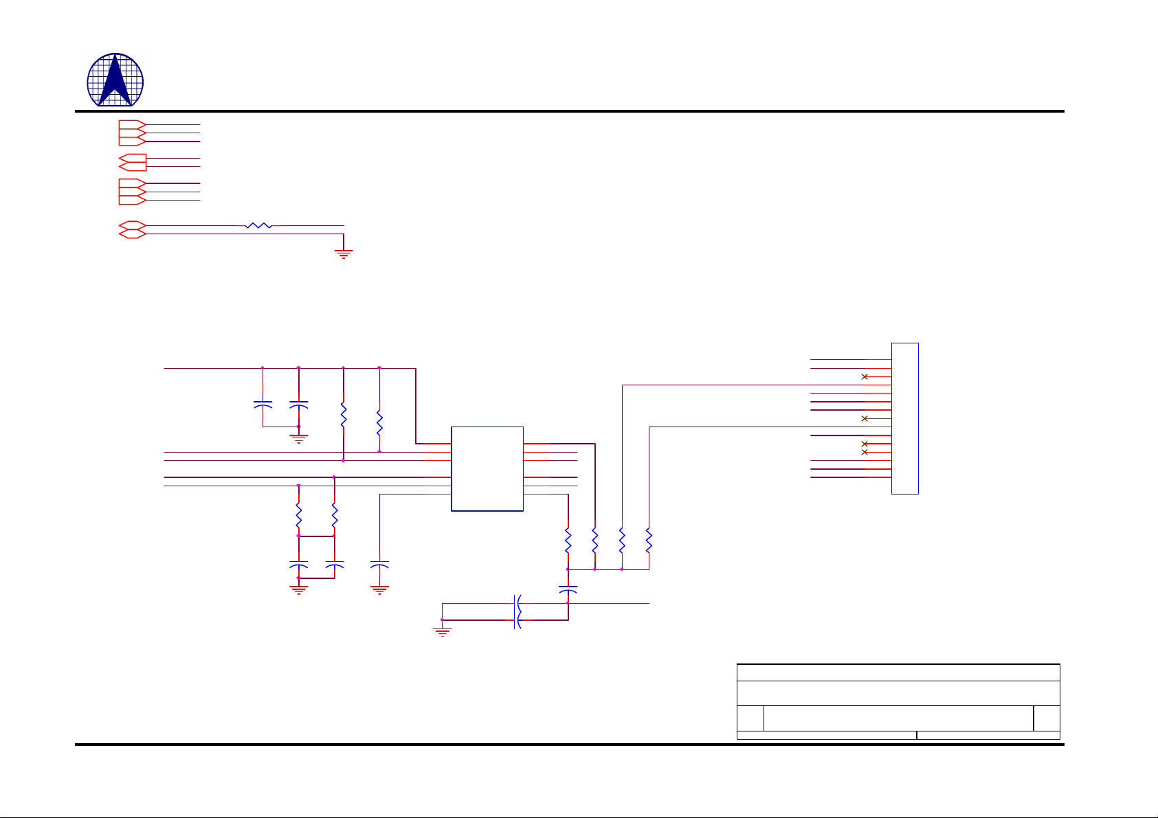
ZVREG
TPOP
TPON
TPIP
TPIN
LNKLED
SPDLED
FULLED
3.3V
GND
AX88790 L 3-in-1 PCMCIA Fast Ethernet Controller
ZVREG
TPOP
TPON
TPIP
TPIN
LNKLED
SPDLED
FULLED
*5 R41 : LED Low Activity be used.
GND
ZVREG
TPOP
TPON
TPIP
TPIN
R41 0
10uF/16V
3.3V_Out
J5
RX-
*6 RECEIVE 1CT : 1CT
TRANSMIT 1CT : 1CT
C2
+
R28
49.9
C26
0.1u
C17
0.1u
R29
49.9
C25
0.001u
R14
49.9
R15
49.9
C24
0.01u
6
7
8
1
2
3
T1
CT
TD+
TD-
RD+
RDCT
16ST0009P
11
CT
10
TX+
9
TX-
16
RX+
15
RX-
14
CT
C16 0.01u
C50 0.01u
TX+
TX-
RX+
RX-
R11
75
C1
0.01u/2KV
R10
75
CHASSIS
R42
75
R43
75
RX+
3.3V_Out
FULLED
LNKLED
SPDLED
GND
TXTX+
15
14
13
12
11
10
9
8
7
6
5
4
3
2
1
PCMCIA15
59
ASIX ELECTRONICS CORPORATION
Title
16ST009P
Size Document Number Rev
790TX1A2.SCH 1.1
A4
Date: Sheet of
3 4Monday, July 10, 2000
ASIX ELECTRONICS CORPORATION
Page 60

J1
1
2
3
4
5
6
7
8
CON8
J3
1
2
3
4
5
6
7
8
CON8
AX88790 L 3-in-1 PCMCIA Fast Ethernet Controller
GND
R45
R78
FULLED
LNKLED
SPDLED
GND
RXRX+
TXTX+
TX+
TX-
RX+
RX-
R45
R78
J2
1
2
3
6
4
5
7
8
RJ45N
FULLED
LNKLED
SPDLED
D2
LED
D5
LED
D6
LED
ON : Full DPX
BLINK : Activity
ON : Link OK
OFF : Link fail
ON : 100M
OFF : 10M
60
ASIX ELECTRONICS CORPORATION
Title
RJ45 CONNECT & LED
Size Document Number Rev
A4
790TX1A3.SCH
Date: Sheet of
4 4Monday, July 10, 2000
ASIX ELECTRONICS CORPORATION
1.1
 Loading...