

Page 1
5-Port 10/100BASE Ethernet Switch Controller
1 Quad RMII/MII PHY
RMII/MII PHY for Down-link or Server
5 Port 10/100Mb SOHO Switch
Features
• Support 5 10/100 Mbps Ethernet ports with
RMII/MII interface
ü Provides packet switching functions between 5
10/100 Mbps, auto-negotiated ports
ü Ideal for SOHO switches and its application
• Build in 5-ports 10/100Mbps Switch engine with
following features
ü Low cost SSRAM interface to reduce system cost
ü One or two 64K*32bit SSRAM to buffer packets
ü 4/8 K MAC address look up Table is supported
ü Address mapping of look up table can be linear or
use hash algorithm
ü Auto learning and filtering
ü Aging the look up table is supported optionally
ü Aging time can be 1min to 640 mins 7 steps
AX88615P
Document No.: AX615-13 / V1.3 / Aug. 11 ’99
ü Three forwarding modes are supported : Store-
and-Forward, Fragment-Free and Auto Forward
which is based on network quality
ü Flow-control is supported optionally
ü 802.3x flow control is supported when running in
full-duplex mode
ü Back-pressure base flow control is supported
when running in half-duplex mode
ü Ext. Buffer Memory auto testing
ü Routing and Learning at wire speed (148800
packets/sec at 100Mbps)
• LED display buffer utilization (%) for whole system
and external SSRAM test.
• Power on LED diagnosis. All the LED display will
follow the “ON-OFF-ON-OFF-Normal” operation
procedure during/after power on reset
• 60MHz Operation, 3.3volt, 208-pin PQFP
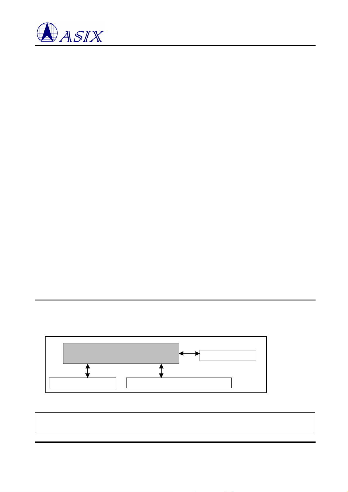
Product description
The AX88615 is a 5-ports 10/100 Mbps Ethernet switch with MII PHY or RMII PHY. It is design for low cost dumb
Switch application, e.g. SOHO Ethernet Switch, with low cost 64K*32 SSRAM buffer memory.
Key Applications
ü SOHO Ethernet Switch
ü IP Router
System Block Diagram
AX88615
Switch Controller
1 or 2 64K*32 SSRAM
This data sheet contains new products information. ASIX ELECTRONICS reserves the rights to modify the product specification without notice. No
Always contact ASIX for possible updates before starting a design.
liability is assumed as a result of the use of this product. No rights under any patent accompany the sale of the product.
ASIX ELECTRONICS CORPORATION First Released Date : APR/02/1999
2F, NO.13, Industry East Rd. II, Science-based Industrial Park, Hsin-Chu City, Taiwan, R.O.C.
TEL: 886-3-579-9500 FAX: 886-3-579-9558 http://www.asix.com.tw
Page 2

CONFIDENTIAL
CONTENTS
1.0 AX88615 OVERVIEW....................................................................................................................................... 4
1.1 GENERAL DESCRIPTION...................................................................................................................................... 4
1.2 AX88615 BLOCK DIAGRAM:.............................................................................................................................. 4
1.3 PIN CONNECTION DIAGRAM ............................................................................................................................... 5
2.0 PIN DESCRIPTION........................................................................................................................................... 6
2.1 MII/RMII INTERFACE FOR SWITCH PORTS............................................................................................................ 6
2.1.1 Switch Port 0.............................................................................................................................................. 6
2.1.2 Switch Port 1.............................................................................................................................................. 7
2.1.3 Switch Port 2.............................................................................................................................................. 7
2.1.4 Switch Port 3.............................................................................................................................................. 8
2.1.5 Switch Port 4.............................................................................................................................................. 8
2.2 LED DISPLAY.................................................................................................................................................... 9
2.3 BUFFER MEMORY PINS GROUP ............................................................................................................................. 9
2.4 MISCELLANEOUS.............................................................................................................................................. 10
2.5 POWER ON CONFIGURATION SETUP SIGNALS CROSS REFERENCE TABLE ................................................................ 11
3.0 FUNCTIONAL DESCRIPTION..................................................................................................................... 13
3.1 BASIC OPERATION............................................................................................................................................ 13
3.2 PACKET FILTERING AND FORWARDING PROCESS................................................................................................ 13
3.3 MAC ADDRESS LEARNING AND AGING PROCESS .............................................................................................. 13
3.4 FLOW CONTROL PROCESS ................................................................................................................................ 13
4.0 INTERNAL REGISTERS................................................................................................................................ 15
5.0 ELECTRICAL SPECIFICATION AND TIMING.......................................................................................... 16
5.1 ABSOLUTE MAXIMUM RATINGS........................................................................................................................ 16
5.2 GENERAL OPERATION CONDITIONS................................................................................................................... 16
5.3 DC CHARACTERISTICS..................................................................................................................................... 16
5.4 AC SPECIFICATIONS......................................................................................................................................... 17
5.4.1 LCLK....................................................................................................................................................... 17
5.4.2 Reset Timing............................................................................................................................................ 17
5.4.3 RMII Interface Timing Tx & Rx ................................................................................................................ 18
5.4.4 MII Interface Timing Tx & Rx.................................................................................................................. 19
5.4.5 SSRAM Read Cycle Timing...................................................................................................................... 20
5.4.6 SSRAM Write CycleTiming....................................................................................................................... 21
5.4.7 LED DISPLAY ......................................................................................................................................... 22
5.4.8 LED Display After Reset.......................................................................................................................... 22
6.0 PACKAGE INFORMATION........................................................................................................................... 23
APPENDIX A: SYSTEM APPLICATIONS.......................................................................................................... 24
A.1 AX88615 AS 5-PORT STANDALONE SOHO SWITCH........................................................................................... 24
A.2 AX88615 FOR IP ROUTER APPLICATION........................................................................................................... 24
A.3 AX88615 AS BACKEND OF DUAL SPEED REPEATERS........................................................................................... 25
APPENDIX B: DESIGN NOTE............................................................................................................................. 26
B.1 USING STATION MANAGEMENT (STA) CONNECTION ........................................................................................ 26
B.2 USING MII I/F CONNECTS TO MAC.................................................................................................................. 26
2
ASIX ELECTRONICS CORPORATION
Page 3

CONFIDENTIAL
FIGURES
FIG - 1 AX88615 BLOCK DIAGRAM ............................................................................................................................. 4
FIG - 2 PIN CONNECTION DIAGRAM.............................................................................................................................. 5
FIG - 3 APPLICATION FOR LED DISPLAY..................................................................................................................... 14
3
ASIX ELECTRONICS CORPORATION
Page 4
CONFIDENTIAL
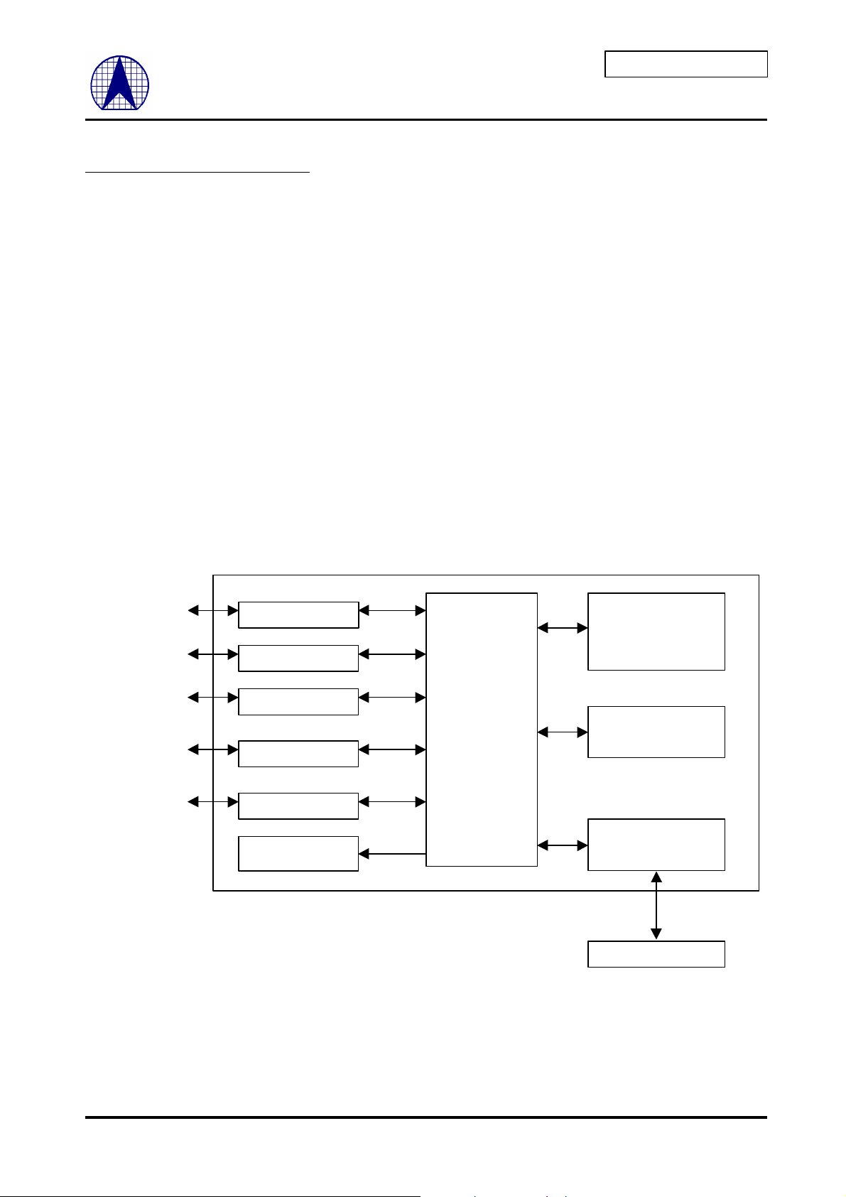
1.0 AX88615 Overview
P0 10/100 MAC
P1 10/100 MAC
P2 10/100 MAC
P3 10/100 MAC
P4 10/100 MAC
PHY
PHY
PHY
PHY
PHY
64K*32 SSRAM
1.1 General Description
The AX88615 is a 5-ports 10/100 Mbps Ethernet switch with MII PHY or RMII PHY. A low cost Fast Ethernet switch
can be implemented by using the AX88615 and low cost 64Kx32 SSRAM .
Data received from the MAC interface is stored in the external memory. All ports support multiple MAC addresses. The
switch provides a look-up table for 8K MAC addresses with two 64Kx32 SSRAMs. The AX88615 provides three frame
forwarding mode: store-and-forward mode, safe cut-through (fragment free) mode and dynamic-select-mode (auto). The
dynamic-select-mode means the switch selects optimizes mode for forwarding packages automatically according to
Network quality.
During transmission, the data is obtained from the buffer memory and routed to the destination port. For half-duplex
operation, the MAC control will back off and retransmit in accordance to the IEEE802.3 CSMA/CD if collision occurs.
The AX88615 provides two flow control methods. For half-duplex operation, an optional jamming based flow control is
available to avoid loss of data. This is also well known as back pressure. In the full-duplex mode, AX88615 utilizes
IEEE802.3X as the flow control mechanism.
1.2 AX88615 Block Diagram:
MII / RMII
MII / RMII
MII / RMII
MII / RMII
MII / RMII
LED Interface
Fig - 1 AX88615 Block Diagram
High Speed
Switch Fabric
Routing /Learning
Controller
Buffer Manager
Buffer Memory
Interface
4
ASIX ELECTRONICS CORPORATION
Page 5

CONFIDENTIAL
1.3 Pin Connection Diagram
VDD
BMA11
BMA10
VSS
VDD
BMA5
BMA1
BMA4
BMA3
BMA2
BMD24
BMD28
BMD27
BMD31
BMD26
BMD25
BMD29
BMD30
SRXD4[3]
SDUPLEX4
SRXD4[1]
STXD4[1]
SCOL4
STXD4[0]
SRXD4[0]
STXCLK4
SRXDV4
SCRS4
SRXD4[2]
STXEN4
SRXCLK4
SRXD3[3]
SDUPLEX3
SRXD3[1]
STXD3[1]
SCOL3
STXD3[0]
SRXD3[0]
STXCLK3
SRXDV3
SCRS3
STXD3[2]
SRXD3[2]
STXEN3
SRXCLK3
STXD3[3]
SDUPLEX1
SDUPLEX0
BMA0
SPEED3
SPEED4
VSS
NC
NC
NC
BMA7
DB_OUT[6]
DB_OUT[5]
DB_OUT[4]
VDD
145
146
147
144
143
101112131415161718
VSS
/BMWE
/BMOE
SPEED2
SCRS2
SRXD2[0]
SRXD2[1]
VDD
STXEN2
BMA8
STXD2[0]
STXD2[1]
SRXCLK2
BMA9
BMD15
BMD14
BMD13
VSS
BMD12
BMD11
BMD10
BMD9
BMD8
BMD7
SRXDV2
SRXD2[2]
SRXD2[3]
SDUPLEX2
VSS
STXD2[2]
STXD2[3]
BMD6
BMD5
BMD4
BMD3
BMD2
BMD1
BMD0
VDD
STXCLK2
BMA16
BMA15
BMA14
BMA13
BMA12
SCOL2
NC
NC
NC
NC
NC
VSS
157
158
159
160
161
162
163
164
165
166
167
168
169
170
171
172
173
174
175
176
177
178
179
180
181
182
183
184
185
186
187
188
189
190
191
192
193
194
195
196
197
198
199
200
201
202
203
204
205
206
207
208
NCNCNCNCNC
153
152
154
155
156
1
56472
3
NC
151
NC
150
DB_OUT[7]
VSS
148
149
8
9
BMA6
BMD16
141
142
BMD20
BMD18
VSS
139
BMD19
138
137
BMD21
135
136
BMD22
BMD23
DB_SEL[7]
133
134
132
DB_SEL[6]
DB_SEL[5]
131
130
BMD17
140
AX88615
19
2324222021
25
26
27
DB_OUT[3]
NCNCNC
DB_SEL[4]
VSS
124
125
126
127
128
129
293028
31
3233343536373839404142
DB_OUT[2]
DB_OUT[1]
DB_OUT[0]
VDD
DB_SEL[3]
121
122
120
119
123
SRXD0[3]
VSS
DB_SEL[2]
DB_SEL[1]
DB_SEL[0]
114
117
115
116
118
4347464445
SRXD0[0]
SRXD0[1]
SRXD0[2]
VSS
110
111
112
113
NC
NCNCNC
106
107
108
109
4849505152
NC
105
104
103
102
101
100
99
98
97
95
94
93
92
91
90
89
88
87
86
85
84
83
82
81
80
79
78
77
76
75
74
73
72
71
70
69
68
67
66
65
64
63
62
61
60
59
58
57
56
55
54
53
96
SRXCLK0
NC
NC
VSS
NC
NC
SRXDV0
SCOL_SP0
SCRS0
NC
STXCLK0
VDD
STXD0[3]
STXD0[2]
STXD0[1]
STXD0[0]
STXEN0
LED_CK
LED<1>
LED<0>
VSS
SRXD1[3]
SRXD1[2]
SRXD1[1]
SRXD1[0]
SRXCLK1
SRXDV1
SCOL_SP1
SCRS1
NC
NC
BMCLK
VSS
LCLK
VDD
REF_CLK
VSS
STXCLK1
STXD1[3]
STXD1[2]
STXD1[1]
STXD1[0]
STXEN1
/RST
/TEST
MDIO
MDC
STXD4[3]
STXD4[2]
Fig - 2 Pin Connection Diagram
5
ASIX ELECTRONICS CORPORATION
Page 6

CONFIDENTIAL
2.0 Pin Description
2.0 Pin Description
The following terms describe the AX88615 pinout:
All pin names with the “/” suffix are asserted low.
I = Input
O = Output
I/O = Input /Output
2.1 MII/RMII interface for switch ports
2.1.1 Switch Port 0
Signal Name Type Pin No. Description
STXEN0 O 87
STXD0[3:0] O 91,90,89,88
STXCLK0 I 93
SDUPLEX0 I 94
SCOL_SP0 I 97
SCRS0
or
SCRS_DV0
SRXDV0 I 98
SRXCLK0 I 104
SRXD0[3:0] I 114,113,
I 96
111,110
Transmit Enable : Active HIGH. This output indicates that the packet
is being transmitted .If MII mode, TXEN0 is synchronous to
STXCLK0. If RMII mode, TXEN0 is synchronous to REF_CLK.
Transmit Data : STXD0[3:0] is synchronous to the rising edge of
STXCLK0 in MII mode. For each STXCLK period in which STXEN is
asserted, TXD[3:0] are accepted for transmission by the PHY.
If RMII mode, STXD0[1:0] is synchronous to REF_CLK. TXD0[1:0]
shall be “00” to indicate idle when TX_EN is disserted. Value that is not
“00” is reserved for out-of-band signaling and shall be ignored by PHY.
When TX_EN is asserted, TXD[1:0] are accepted for transmission by
PHY
Transmit Clock : Provides the timing reference for the STXEN0,
STXD0 signals in MII mode. STXCLK0 frequency is one fourth of the
data rate (25 MHz for 100Mbps, 2.5 MHz for 10Mbps).
Duplex Select : DUPLEX0 is not standard MII/RMII signal. This input
is connected to PHY directly to obtain the current data rate of Port0.
Collision Detect: Active HIGH. Indicates a collision has been detected
on wire in MII mode. This input is not synchronous to any clock and
ignored in full-duplex mode
If RMII mode, the signal is a speed indicator. Active for 10Mbps speed
is selected depending on power on configuration.
Carrier Sense : Active HIGH. Indicates that either the transmit or
receive medium is non-idle in MII mode. SCRS0 is not synchronous to
any clock.
When RMII mode, the input is CRS_DV (Carrier Sense/Receive Data
Valid ) that is asserted asynchronously on detection of carrier by the
PHY when receive medium is non-idle. Loss of carrier shall result in
the desertion of CRS_DV synchronous to the cycle of REF_CLK, which
presents the first DI-bit of a nibble on to RXD0[1:0].
Receive Data Valid : Active HIGH. Indicates that valid data is present
on the SRXD0 lines. Synchronous to SRXCLK0.
Receive Clock : Provides the timing reference for the SRXDV0,
SRXD0 signals in MII mode. STXCLK0 frequency is one fourth of the
data rate (25 MHz for 100Mbps, 2.5 MHz for 10Mbps).
Receive Data : Synchronously to the rising edge of RXCLK in MII
mode.
If RMII mode, SRXD0[1:0] is synchronous to REF_CLK. SRXD0[1:0]
shall be “00” to indicate idle when CRS_DV is disserted. Value that is
not “00” is reserved for out-of-band signaling shall be ignored by MAC
Upon assertion of CRS_DV, PHY shall ensure that RXD[1:0] = “00”
until proper receive decoding takes place
6
ASIX ELECTRONICS CORPORATION
Page 7
CONFIDENTIAL
2.1.2 Switch Port 1
Signal Name Type Pin No. Description
STXEN1 O 60
STXD1[3:0] O 64,63,62,61
STXCLK1 I 65
SDUPLEX1 I 66
SCOL_SP1 I 76
SCRS1
or
SCRS_DV1
SRXDV1 I 77
SRXCLK1 I 78
SRXD1[3:0] I 82,81,80,79
I 75
Transmit Enable : Please references section 2.1.1 SWITCH PORT0
description.
Transmit Data : Please references section 2.1.1 SWITCH PORT0
description.
Transmit Clock : Please references section 2.1.1 SWITCH PORT0
description.
Duplex Select : Please references section 2.1.1 SWITCH PORT0
description.
Collision Detect: Please references section 2.1.1 SWITCH PORT0
description.
Carrier Sense : Please references section 2.1.1 SWITCH PORT0
description.
Receive Data Valid : Please references section 2.1.1 SWITCH PORT0
description.
Receive Clock : Please references section 2.1.1 SWITCH PORT0
description.
Receive Data : Please references section 2.1.1 SWITCH PORT0
description.
2.1.3 Switch Port 2
Signal Name Type Pin No. Description
STXEN2 O 165
STXD2[3:0] O 187,186,
168,167
STXCLK2 I 196
SDUPLEX2 I 184
SCOL2 I 202
SCRS2
or
SCRS_DV2
SRXDV2 I 181
SRXCLK2 I 169
SRXD2[3:0] I 183,182,
SPEED2 I 160
I 161
163,162
Transmit Enable : Please references section 2.1.1 SWITCH PORT0
description.
Transmit Data : Please references section 2.1.1 SWITCH PORT0
description.
Transmit Clock : Please references section 2.1.1 SWITCH PORT0
description.
Duplex Select : Please references section 2.1.1 SWITCH PORT0
description.
Collision Detect: Please references section 2.1.1 SWITCH PORT0
description.
Carrier Sense : Please references section 2.1.1 SWITCH PORT0
description.
Receive Data Valid : Please references section 2.1.1 SWITCH PORT0
description.
Receive Clock : Please references section 2.1.1 SWITCH PORT0
description.
Receive Data : Please references section 2.1.1 SWITCH PORT0
description.
Speed Indicator : Identify data rate of Port 2
7
ASIX ELECTRONICS CORPORATION
Page 8

CONFIDENTIAL
2.1.4 Switch Port 3
Signal Name Type Pin No. Description
STXEN3 O 5
STXD3[3:0] O 15,14,7,6
STXCLK3 I 33
SDUPLEX3 I 13
SCOL3 I 34
SCRS3
or
SCRS_DV3
SRXDV3 I 10
SRXCLK3 I 9
SRXD3[3:0] I 12,11,4,3
SPEED3 I 1
I 2
Transmit Enable : Please references section 2.1.1 SWITCH PORT0
description.
Transmit Data : Please references section 2.1.1 SWITCH PORT0
description.
Transmit Clock : Please references section 2.1.1 SWITCH PORT0
description.
Duplex Select : Please references section 2.1.1 SWITCH PORT0
description.
Collision Detect: Please references section 2.1.1 SWITCH PORT0
description.
Carrier Sense : Please references section 2.1.1 SWITCH PORT0
description.
Receive Data Valid : Please references section 2.1.1 SWITCH PORT0
description.
Receive Clock : Please references section 2.1.1 SWITCH PORT0
description.
Receive Data : Please references section 2.1.1 SWITCH PORT0
description.
Speed Indicator : Identify data rate of Port 3
2.1.5 Switch Port 4
Signal Name Type Pin No. Description
STXEN4 O 45
STXD4[3:0] O 55,54,47,46
STXCLK4 I 36
SDUPLEX4 I 53
SCOL4 I 37
SCRS4
or
SCRS_DV4
SRXDV4 I 50
SRXCLK4 I 49
SRXD4[3:0] I 52,51,44,43
SPEED4 I 41
I 42
Transmit Enable : Please references section 2.1.1 SWITCH PORT0
description.
Transmit Data : Please references section 2.1.1 SWITCH PORT0
description.
Transmit Clock : Please references section 2.1.1 SWITCH PORT0
description.
Duplex Select : Please references section 2.1.1 SWITCH PORT0
description.
Collision Detect: Please references section 2.1.1 SWITCH PORT0
description.
Carrier Sense : Please references section 2.1.1 SWITCH PORT0
description.
Receive Data Valid : Please references section 2.1.1 SWITCH PORT0
description.
Receive Clock : Please references section 2.1.1 SWITCH PORT0
description.
Receive Data : Please references section 2.1.1 SWITCH PORT0
description.
Speed Indicator : Identify data rate of Port 4
8
ASIX ELECTRONICS CORPORATION
Page 9

CONFIDENTIAL
2.2 LED Display
Signal Name Type Pin No. Description
LED[1:0] O 85, 84
SSRAM Fail / Buffer Memory Utilization LED :
v As utilization of buffer memory
The buffer utilization of switch uses the following definition:
1: Led off
0: Led on
Utilization (%) UTI0 UTI1 UTI2 UTI3 UTI4 UTI5
0 1 1 1 1 1 1
10 0 1 1 1 1 1
20 0 0 1 1 1 1
40 0 0 0 1 1 1
60 0 0 0 0 1 1
80 0 0 0 0 0 1
95 0 0 0 0 0 0
For detail , see the LED timing specification.
v SSRAM Fail
LED[0] : This signal also indicates SRAM chip 0 fail ( continue active low )
during the interval of sequence shift data.
LED[1] : This signal also indicates SRAM chip 1 fail ( continue active low )
during the interval of sequence shift data.
LED_CK O 86
LED Clock : The signal is a discontinue clock for LED signals serial shift
out. The clock period width is 400nS and last 32 cycle with every 52.4ms
repeated.
2.3 Buffer memory pins group
Signal Name Type Pin No. Description
BMA[16:0] O 197–201
16,17
170,166
143,142
23-18
BMD[31:24]
BMD[23:16]
BMD[15:8]
BMD[7:0]
/BMWE O 158
/BMOE O 159
BMCLK O 72
I/O 24, 26-32
133-138
140, 141
171-173
175-179
180,
188-194
SSRAM Address Bus
SSRAM Data Bus
SSRAM Write Strobe
SSRAM Read Strobe
SSRAM CLOCK
9
ASIX ELECTRONICS CORPORATION
Page 10

CONFIDENTIAL
2.4 Miscellaneous
Signal Name Type Pin No. Description
LCLK I 70
/RST I 59
REF_CLK I 68
/TEST I/PU 58
MDIO I/O 57
MDC O 56
DB_SEL[7:0] I/PU 132-129,
119-116
DB_OUT[7:0] O 148-145,
124,123,
121,120
NC O 38,39,40,
56,57,73,
74,95,99,
100,102,
105-109,
125,126,
128,
150-156,
203-207
VDD I 25, 48,
69, 92,
122, 144,
164, 195,
VSS I 8, 35,
67, 71,
83, 101,
112,115,
127, 139,
149, 157,
174,185,
208
Local Clock : 66Mhz. Used for system operation synchronous.
Reset : Active Low
The chip is reset when this signal is asserted Low.
Reference clock : The input is a continue clock at 50Mhz for timing
reference with RMII interface.
Test Pin : Active LOW
The pin is just for test mode setting purpose only. Must be pull high when
normal operation.
Station Management Data In/Out :
To read PHY Auto Negotiation Remote Capability register to get current
speed and duplex status. (See appendix also)
Station Management Data Clock Out : For MDIO reference clock.
Debug Mode Selection :
Enable debug selection when /TEST pin = 0
Debug Mode Monitor Output :
NC : Keep no connection
POWER : +3.3V +/-5%
POWER: 0V
10
ASIX ELECTRONICS CORPORATION
Page 11

CONFIDENTIAL
2.5 Power on configuration setup signals cross reference table
Signal Name Share with Description
/Hash_En BMA[16]
Aging_S[2:0] BMA[15:13]
RxFC_En BMA[12]
MII_S1 BMA[11]
MII_S0 BMA[10]
/Part_En BMA[9]
RAM_S BMA[5]
NetQlty_S BMA[4]
FwTyp_S1
FwTyp_S0
HiBndy_S1
HiBndy_S0
/ FlowCtl _En4 STXEN0
/ FlowCtl _En3 STXD0[3]
BMA[3]
BMA[2]
BMA[1]
BMA[0]
Hash Algorithm Enable :
0 : Enable look-up table addressing use hashing algorithm.
1 : Disable look-up table addressing use linear addressing
Aging Timer Selection :
Aging_S2 Aging_S1 Aging_S0 Aging Time (Min)
1 1 1 no aging (disable)
1 1 0 5
1 0 1 10
1 0 0 20
0 1 1 40
0 1 0 160
0 0 1 640
0 0 0 1
PAUSE Identification Enable :
0 : Disable 802.3x receives flow control function in full duplex.
1 : Enable 802.3x receives flow control function in full duplex.
MII Enable for Port 1, 2, 3, 4 :
0 : Switch port 1, 2, 3, 4 “RMII” mode is selected
1 : Switch port 1, 2, 3, 4 “MII” mode is selected
MII Enable for Port 0 :
0 : Switch port 0 “RMII” mode is selected
1 : Switch port 0 “MII” mode is selected
TX Partition Enable :
0 : Enable partition function of transition.
1 : Disable partition function of transition.
RAM Size Selection : External packet buffer RAM size select
RAM_S RAM SIZE
1 64K * 32 SSRAM
0 128K * 32 SSRAM
Network Quality Selection: Auto forwarding mode is based on packet error
percentage to select Store-and-Forward or Fragment Free mode.
NetQlty_S Error Packet Ratio
1 20%
0 40%
Forward Type Selection :
FwTyp _S1 FwTyp _S0 Forward Mode
1 1 Store & Forward
1 0 Store & Forward
0 1 Fragment Free
0 0 Auto
Threshold Selection for Flow Control :
Flow control will be active when buffer memory is below the threshold:
HiBndy_S1 HiBndy_S0 Buffers Left
1 1 64 packets
1 0 32 packets
0 1 16 packets
0 0 96 packets
P4 Flow Control Enable :
Enable flow control function of switch port 4, 802.3x for full duplex, back
pressure for half duplex.
0 : Enable flow control function.
1 : Disable flow control function.
P3 Flow Control Enable : Enable flow control functions of switch port 3,
11
ASIX ELECTRONICS CORPORATION
Page 12

CONFIDENTIAL
802.3x for full duplex, back pressure for half duplex.
0 : Enable flow control function.
1 : Disable flow control function.
/ FlowCtl _En2 STXD0[2]
/ FlowCtl _En1 STXD0[1]
/FlowCtl_En0 STXD0[0]
Speed_S1 STXD1[2]
Speed_S0 STXD1[1]
FdpxHi_S1 STXD1[0]
FdpxHi_S0 STXEN1
/RdPhy_En STXD4[0]
PktLenOpt STXD3[0]
P2 Flow Control Enable : Enable flow control functions of switch port 2,
802.3x for full duplex, back pressure for half duplex.
0 : Enable flow control function.
1 : Disable flow control function.
P1 Flow Control Enable : Enable flow control functions of switch port 1,
802.3x for full duplex, back pressure for half duplex.
0 : Enable flow control function.
1 : Disable flow control function.
P0 Flow Control Enable : Enable flow control functions of switch port 0,
802.3x for full duplex, back pressure for half duplex.
0 : Enable flow control function.
1 : Disable flow control function.
Speed Setting for Port 1, 2, 3, 4 : In RMII mode, speed “SCOL_SP1” pin
function selection
0 : Port 1, 2, 3, 4 RMII mode, SCOL_SP1 pin is Low for 10M,high for 100M
1 : Port 1, 2, 3, 4 RMII mode, SCOL_SP1 pin is Low for 100M,high for 10M
Speed Setting for Port 0 : In RMII mode, speed “SCOL_SP0” pin function
selection
0 : Port 0 RMII mode, SCOL_SP0 pin is Low for 10M,high for 100M
1 : Port 0 RMII mode, SCOL_SP0 pin is Low for 100M,high for 10M
Duplex Setting for Port 1, 2, 3, 4 : Port 1, 2, 3, 4 “SDUPLEX1” pin function
select
0 : SDUPLEX1 pin is Low for half duplex,high for full duplex
1 : SDUPLEX1 pin is Low for full duplex,high for half duplex
Duplex Setting for Port 0 : Port 0 “SDUPLEX0” pin function selection
0 : SDUPLEX0 pin is Low for half duplex,high for full duplex
1 : SDUPLEX0 pin is Low for full duplex,high for half duplex
MDIO read PHY Register 05h Information
0 : Enable
1 : Disable
Maximun Packet Length Selection
0 : 1522 Byte
1 : 1518 Byte
All of the above signals are pull-up for default values.
12
ASIX ELECTRONICS CORPORATION
Page 13

CONFIDENTIAL
3.0 Functional Description
3.1 Basic Operation
In general, the basic operation of the switch is very simple. The switch receives incoming packets from one of its ports,
searches in the Look-Up Table for the Destination MAC Address and then forwards the packet to the destination ports,
if appropriate. If the destination MAC address is not found in the Look-Up Table, the switch treats the incoming packet
as a broadcast packet and forwards it to all ports except itself. Basically the switch automatically learns the port number
of attached network devices by examining the Source MAC Address of all incoming packets. The device is updated the
table with the Source MAC Address if the Source MAC Address does not exist the table.
3.2 Packet Filtering and Forwarding Process
During the receiving process, the switch will monitor the length of the received packet. Legal Ethernet packets should
have a length of no less 64 bytes and nor more than 1528 bytes. The switch discards any packet with illegal length.
After a packet is received, its Source MAC Address and Destination MAC Address are received. The Source MAC
Address is used to update the Look-Up Table and the Destination MAC Address is used to determine the destination port
of the packet. Once a MAC Address has been learned, and the packet is buffered, it must be forwarded, That is, the packet
forwarding mechanism for the switch is handled automatically based on the destination MAC Address.
Under the following conditions, received packets are filtered:
¨ The switch will check all received packets for errors, e.g., FCS error, runt packet, long packet, etc.
¨ Any packet handing to its own source port will be filtered. That is, its destination port is its source port.
¨ The incoming packet will be discarded if the switch’s buffer memory is full.
The switch supports three forwarding modes: Store-and-Forward, Fragment-Free and Auto.
¨ Store-and-Forward Mode: An entry packet is received, checked and stored in the buffer memory before it
is forwarded. That is, each forwarded packet is correct.
¨ Fragment-Free Mode: It is a simple improvement on Cut-Through method. The switch will forward a
packet whose packet length is more than 64 bytes. All runt packets will be filtered in Fragment-Free
mode.
¨ Auto Mode: In Auto mode, the switch select dynamically its optimized forwarding mode based on the
current network quality of each port.
3.3 MAC Address Learning and Aging Process
The switch can learn up to 8K unique MAC addresses with a hashing algorithm. Addresses are stored in the Look-Up
Table located in external SSRAM, then each packet updates the table.
The table lookup engine provides the switching information required routing the data packets. The address table is set up
through auto address learning dynamically. After the switch receives a packet, the Source MAC Address and Destination
MAC Address are received. The Source Address retrieved from the received packet is automatically stored in a SA
buffer. The switch will check for error and perform a SA search. The switch will update the Look-Up Table with the
Source MAC Address if there is no error.
The Look-Up Table is cleared on power-on, or hardware reset. When the aging option is enabled, the dynamically
Learned SA will be cleared if it is not refreshed in less than configured time (2 or 5 min).
3.4 Flow Control Process
The switch can operate at two different modes: half-duplex and full-duplex. Each port can be configured to have flow
control enabled or not. The switch supports 802.3X for full-duplex operation and uses back pressure for half-duplex.
In full-duplex mode, the switch will receive and transmit the packet in accordance to 802.3X. The transmission channel
and the receiving channel operate independently. If the occupancy of the buffer memory is above the FlowControlActive
13
ASIX ELECTRONICS CORPORATION
Page 14

CONFIDENTIAL
threshold, the MAC of port will send out a PAUSE frame with maximum delay. The switch will send out a PAUSE
frame with zero delay after below FlowControlActive threshold.
For the receiving channel, the switch will not transmit the next packet whenever received a PAUSE frame with non-zero
delay. The switch will resume packet transmission either after the pause timer expired or a PAUSE frames with zero
delay received.
In half-duplex mode, the switch will receive and transmit the packet in accordance to 802.3 CSMA/CD. If the occupancy
of the buffer memory is above the FlowControlActive threshold, the MAC of port will send out JAM pattern .
3.5 LED Display Interface
AX88615 provides LED status indication for memory test and packet buffer utilization (%). All LED[2:0]
perform active low.
LED[2:0] Status Driver Wave-form as follows :
LED_CK
D0 D1 D2 D3 D4 D5 D6 D7 D8 D9 D11 D12 D13 D14D10 D15
LED[0]
N/A
D16 D19 D20 D21 D22D18 D23D17 ( This portation no clock presented )
LED[0]
N/AN/AN/AN/AN/A
N/A
N/AN/A
Chip 0 Memory Test Fail and/or 100M Collision
Continue
LED[1]
LED[1]
N/A
N/AN/AN/AN/AN/AN/AN/AN/AN/AN/A
N/AN/AN/AN/AN/AN/AN/A
Chip 1 Memory Test Fail and/or 10M Collision
UTI5
UTI4
UTI3
UTI2
SW
SW
SW
SW
Continue
It must use external shift register to decode data on LED[1]. The application shows as follows:
SW UTI2
SW UTI1
Q
Q
5
6
SW UTI0
Q
7
LED[1]
LED_CK
Q
0
D
Q1Q2Q
74LS164(#1)
SW UTI5
SW UTI4
SW UTI3
Q
4
3
Q
Q
Q
7
5
6
Q
0
Q1Q2Q
D
Q
4
3
74LS164(#2)
SW
UTI1
N/AN/AN/AN/AN/AN/AN/AN/AN/AN/AN/AN/AN/AN/AN/A
SW
UTI0
Fig - 3 Application for LED display
14
ASIX ELECTRONICS CORPORATION
Page 15

CONFIDENTIAL
4.0 INTERNAL REGISTERS
(This page keep blank)
15
ASIX ELECTRONICS CORPORATION
Page 16

CONFIDENTIAL
5.0 ELECTRICAL SPECIFICATION AND TIMING
5.1 Absolute Maximum Ratings
Description SYM Min Max Units
Operating Temperature Ta 0 +70
Storage Temperature Ts -55 +150
Supply Voltage Vcc -0.3 +4.0 V
Input Voltage Vin -0.3 Vdd+0.5 V
Output Voltage Vout -0.3 Vdd+0.5 V
Lead Temperature (soldering 10 seconds maximum) Tl -55 +220
Note : Stress above those listed under Absolute Maximum Ratings may cause permanent damage to the device. Exposure
to Absolute Maximum Ratings conditions for extended period, adversely affect device life and reliability
5.2 General Operation Conditions
Description SYM Min Max Units
Operating Temperature Ta 0 +70
Supply Voltage Vdd +3.0 +3.6 V
5.3 DC Characteristics
(Vdd=3.0V to 3.6V, Vss=0V, Ta=0°C to 70°C)
Description SYM Min Max Units
Low Input Voltage Vil Vss-0.3 0.8 V
High Input Voltage Vih 2 Vdd+0.5 V
Low Output Voltage Vol 0.4 V
High Output Voltage Voh 2.4 V
Input Leakage Current 1 (Note 1) Iil1 10 uA
Input Leakage Current 2 (Note 2) Iil1 500 uA
Output Leakage Current Iol 10 uA
°C
°C
°C
°C
Description SYM Min Tpy Max Units
Power Consumption Pc TBD mA
Note :
1. All the input pins without pull low or pull high.
2. Those pins had been pull low or pull high.
16
ASIX ELECTRONICS CORPORATION
Page 17

CONFIDENTIAL
5.4 AC specifications
5.4.1 LCLK
Thigh
LCLK
Tr Tf Tlow
Tcyc
BMCLK Tod
Symbol Description Min Typ. Max Units
Tcyc CYCLE TIME
Thigh CLK HIGH TIME
Tlow CLK LOW TIME
Tr/Tf CLK SLEW RATE
Tod LCLK TO BMCLK OUT DELAY
5.4.2 Reset Timing
6.64 8.3 9.96 ns
6.64 8.3 9.96 ns
1 - 4 ns
16.6 ns
2 ns
REF_CLK
/RST
Symbol Description Min Typ. Max Units
Trst Reset pulse width
10 - - REF_Clk
17
ASIX ELECTRONICS CORPORATION
Page 18

CONFIDENTIAL
5.4.3 RMII Interface Timing Tx & Rx
T0 T1
REF_CLK
T2 T3
TX_EN
TXD
CRS_DV
T2 T3
RXD
Symbol Description Min Typ. Max Units
T0 REF_CLK Clock Cycle Time 19.998 20 20.002 ns
T1 REF_CLK Clock High Time 7 10 13 ns
T2 CRS_DV, RXD, TXEN and TXD data setup to
REF_CLK rising edge
T3 CRS_DV, RXD, TXEN and TXD data hold from
REF_CLK rising edge
4 ns
2 ns
18
ASIX ELECTRONICS CORPORATION
Page 19

CONFIDENTIAL
5.4.4 MII Interface Timing Tx & Rx
T0 T1
TXCLK
T2 T2
TX_EN
T3 T3
TXD
Symbol Description Min Typ. Max Units
T0 TXCLK Cycle Time 39.996 40 40.004 ns
T1 TXCLK High Time 14 20 26 ns
T2 TX_EN Delay from TXCLK High 7.440 21.760 ns
T3 TXD Delay from TXCLK High 3.410 13.320 ns
T4 T5
RX_CLK
CRS
T6
RXDV
T7
RXD
RXER
Symbol Description Min Typ. Max Units
T4 RX_CLK Clock Cycle Time 39.996 40 40.004 ns
T5 RX_CLK Clock High Time 14 20 26 ns
T6 CRS to RXDV Delay Requirement 40 160 ns
T7 RXD or RXDV setup to RX_CLK rise time 10 - ns
19
ASIX ELECTRONICS CORPORATION
Page 20

CONFIDENTIAL
5.4.5 SSRAM Read Cycle Timing
T5
T4D1T3A1T2
T1
BMCLK
BMA[16:0]
/BMWR
/BMOE
BMD[7:0]
Symbol Description Min Max Units
T1 Clock Cycle Time 15 - ns
T2 Address Bus Setup Time 2.5 - ns
T3 Address Bus Hold Time 0.5 - ns
T4 Clock to Output Invalid 2 - ns
T5 Clock to Output Valid - 6 ns
20
ASIX ELECTRONICS CORPORATION
Page 21

CONFIDENTIAL
5.4.6 SSRAM Write CycleTiming
T5
T4A1T3
T2T1D1
BMCLK
BMA[16:0]
/BMWR
/BMOE
BMD[7:0]
Symbol Description Min Max Units
T1 Clock Cycle Time 15 - ns
T2 Address Bus Setup Time 2.5 - ns
T3 Address Bus Hold Time 0.5 - ns
T4 Write Data Setup Time 2.5 - ns
T7 Write Data Hold Time 0.5 - ns
21
ASIX ELECTRONICS CORPORATION
Page 22

CONFIDENTIAL
5.4.7 LED DISPLAY
T4
T1
LED_CK
--------
D0 D1 D2 .............. D22 D23
LED_CK
LED[1:0]
~
~
-------
-
D0 D1 D2
Symbol Description Min Typ. Max Units
T1 LED_CK Clock Cycle Time 400 ns
T2 Clock to Output Valid 206.5 ns
T3 Clock to Output Invalid 200 ns
T4 continuous 32 LED_CK Cycle Time 52.4 ms
5.4.8 LED Display After Reset
/Reset
T1 T2 T2 T2 T3
LED[1:0]
Symbol Description Min Typ. Max Units
T1 Repeater reset time 1000 ns
T2 LED Blink Time After Reset 838.4 ms
T3 LED Dark Time Before Normal Display 419.2 ms
22
ASIX ELECTRONICS CORPORATION
Page 23

CONFIDENTIAL
6.0 PACKAGE INFORMATION
Hd
D
pin 1
He
E
b
e
A2 A1
L1
L
θ
MILIMETERSYMBOL
MIN. NOM MAX
A1 0.05 0.25 0.5
A2 3.17 3.32 3.47
b 0.10 0.20 0.30
D 27.90 28.00 28.10
E 27.90 28.00 28.10
e 0.50
Hd 30.35 30.60 30.85
He 30.35 30.60 30.85
L 0.45 0.60 0.75
L1 1.30
θ
0 10
23
ASIX ELECTRONICS CORPORATION
Page 24

CONFIDENTIAL
Appendix A: System Applications
Quad RMII PHY
Single PHY
A.1 AX88615 as 5-port standalone SOHO switch
AX88615
Switch Controller
A.2 AX88615 for IP router application
Quad RMII PHY
AX88615
Switch Controller
AX88195 or AX88196
Local CPU Bus MAC
controller
24
ASIX ELECTRONICS CORPORATION
Page 25

CONFIDENTIAL
A.3 AX88615 as backend of dual speed repeaters
10Mbps and 100Mbps horizontal cascade
10Mbps and 100Mbps Vertical cascade upto 4 stacks
10Mbps and 100Mbps horizontal
2 Quad RMII PHY
2 Quad RMII PHY
Quad PHY
Single PHY
10M Link
100M
Buffer
AX88873 #1
Repeater Controller
2 Quad RMII PHY 2 Quad RMII PHY
Buffer
AX88873 #1
Repeater Controller
AX88873 #0
Repeater Controller
AX88873 #0
Repeater Controller
5-port Switch Controller
AX88615
25
ASIX ELECTRONICS CORPORATION
Page 26

CONFIDENTIAL
Appendix B: Design Note
Clock
BMA[10]
STXEN1
B.1 Using Station Management (STA) Connection
There are two methods to get per port speed and duplex information in AX88615 . One way is by hardware pins such as
SPEED0, SDUPLEX0, SPEED1, SDUPLEX1. Ax88615 also provides 2 pins (MDC and MDIO, STA – Station
Management connection) to read PHY Auto Negotiation Remote Capability register to get current speed and duplex
status. When use STA function, the connected PHY address settings must be fixed as follows:
Port 0 Port 1 Port 2 Port 3 Port 4
0fh 10h 11h 12h 13h
The corresponding option setting
/RdPhy_En = 0
B.2 Using MII I/F connects to MAC
Using MII interface to connect to MAC type device application for AX88615 is illustrated bellow.
3.3V
10K * 2
SDUPLEX0
SCOL_SP0
STXEN0
STXCLK0
STXD0[3:0]
SCRS0
SRXDV0
SRXCLK0
SRXD0[3:0]
10K
Gnd
25MHz
COL
CRS
RX_DV
RX_CLK
RXD[3:0]
RX_ER
TX_EN
TX_CLK
TXD[3:0]
TX_ER
AX88615 / Switch AX88195 / MAC
Note : 1. The MAC needs to run at fullduplex mode.
2. Care must be taken that the receive side has enough setup and/or hold time
3. Some kind of CPU with embbeded MAC can also refer to this example
26
ASIX ELECTRONICS CORPORATION
 Loading...