

Page 1
Features
CPU
LATCH
Addr L
Addr H
Ctl BUS
SRAM
AX88195P
10/100BASE Local CPU Bus Fast Ethernet MAC Controller
Document No.: AX195-17 / V1.7 / May. 12 ’00
• IEEE 802.3u 100BASE-T, TX, and T4 Compatible
• Single chip local CPU bus 10/100Mbps Fast
Ethernet MAC Controller
• NE2000 register level compatible instruction
• Support both 8 bit and 16 bit local CPU interfaces
include MCS-51 series, 80186 series and MC68K
series CPU
• Support both 10Mbps and 100Mbps data rate
• Support both full-duplex or half-duplex operation
• Provides a MII port for both 10/100Mbps operation
• External and internal loop-back capability
• Two external 32K*8 Asynchronous SRAMs
required for packet buffer
• 128-pin LQFP low profile package
• 25MHz Operation, Dual 5V and 3.3V CMOS
process with 5V I/O tolerance. Or pure 3.3V
operation
*IEEE is a registered trademark of the Institute of Electrical and Electronic
Engineers, Inc.
*All other trademarks and registered trademark are the property of their
respective holders.
• Support EEPROM interface to store MAC address
Product description
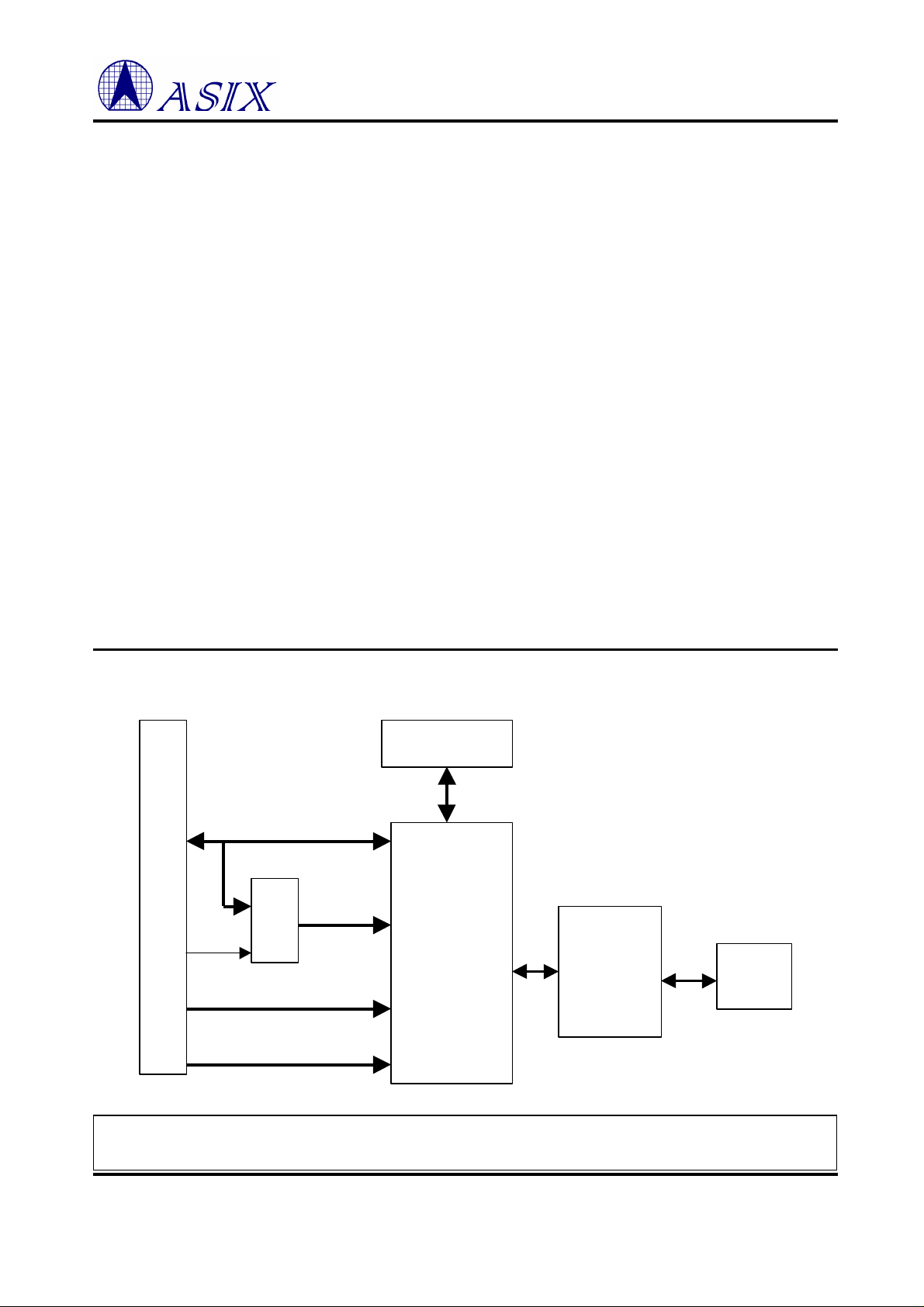
The AX88195 Fast Ethernet Controller is a high performance and highly integrated local CPU bus Ethernet Controller.
The AX88195 supports both 8 bit and 16 bit local CPU interfaces include MCS-51 series, 80x86 series, MC68K series
CPU and ISA bus. The AX88195 implements both 10Mbps and 100Mbps Ethernet function based on IEEE802.3 /
IEEE802.3u LAN standard and supports both 10Mbps/100Mbps media-independent interface (MII) to simplify the
design. Two low cost 32k*8 SRAM is required for packet buffer.
System Block Diagram
BUFFER
AD BUS
AX88195
PHY/TxRx RJ45
Always contact ASIX for possible updates before starting a design.
This data sheet contains new products information. ASIX ELECTRONICS reserves the rights to modify product specification without notice. No liability
is assumed as a result of the use of this product. No rights under any patent accompany the sale of the product.
ASIX ELECTRONICS CORPORATION First Released Date : Oct/02/1998
2F, NO.13, Industry East Rd. II, Science-based Industrial Park, Hsin-Chu City, Taiwan, R.O.C.
TEL: 886-3-579-9500 FAX: 886-3-579-9558 http://www.asix.com.tw
Page 2

AX88195 Local CPU Bus Fast Ethernet MAC Controller
CONTENTS
1.0 INTRODUCTION .............................................................................................................................................. 4
1.1 GENERAL DESCRIPTION:..................................................................................................................................... 4
1.2 AX88195 BLOCK DIAGRAM:.............................................................................................................................. 4
1.3 AX88195 PIN CONNECTION DIAGRAM ............................................................................................................... 5
1.3.1 AX88195 Pin Connection Diagram for ISA Bus Mode................................................................................ 6
1.3.2 AX88195 Pin Connection Diagram for 80x86 Mode ................................................................................... 7
1.3.3 AX88195 Pin Connection Diagram for MC68K Mode................................................................................ 8
1.3.4 AX88195 Pin Connection Diagram for MCS-51 Mode ............................................................................... 9
2.0 SIGNAL DESCRIPTION................................................................................................................................. 10
2.1 LOCAL CPU BUS INTERFACE SIGNALS GROUP................................................................................................... 10
2.2 MII INTERFACE SIGNALS GROUP........................................................................................................................ 11
2.3 EEPROM SIGNALS GROUP .............................................................................................................................. 12
2.4 SRAM INTERFACE PINS GROUP......................................................................................................................... 12
2.5 MISCELLANEOUS PINS GROUP............................................................................................................................ 12
2.6 POWER ON CONFIGURATION SETUP SIGNALS CROSS REFERENCE TABLE ................................................................ 13
3.0 MEMORY AND I/O MAPPING...................................................................................................................... 14
3.1 EEPROM MEMORY MAPPING.......................................................................................................................... 14
3.2 I/O MAPPING................................................................................................................................................... 14
3.3 SRAM MEMORY MAPPING .............................................................................................................................. 14
4.0 REGISTERS OPERATION............................................................................................................................. 15
4.1 COMMAND REGISTER (CR) OFFSET 00H (READ/WRITE)................................................................................... 17
4.2 INTERRUPT STATUS REGISTER (ISR) OFFSET 07H (READ/WRITE)..................................................................... 17
4.3 INTERRUPT MASK REGISTER (IMR) OFFSET 0FH (WRITE)................................................................................. 18
4.4 DATA CONFIGURATION REGISTER (DCR) OFFSET 0EH (WRITE)....................................................................... 18
4.5 TRANSMIT CONFIGURATION REGISTER (TCR) OFFSET 0DH (WRITE)................................................................ 18
4.6 TRANSMIT STATUS REGISTER (TSR) OFFSET 04H (READ) ................................................................................ 19
4.7 RECEIVE CONFIGURATION (RCR) OFFSET 0CH (WRITE) .................................................................................. 19
4.8 RECEIVE STATUS REGISTER (RSR) OFFSET 0CH (READ) .................................................................................. 19
4.9 INTER-FRAME GAP (IFG) OFFSET 16H (READ/WRITE) ...................................................................................... 20
4.10 INTER-FRAME GAP SEGMENT 1(IFGS1) OFFSET 12H (READ/WRITE)............................................................... 20
4.11 INTER-FRAME GAP SEGMENT 2(IFGS2) OFFSET 13H (READ/WRITE)............................................................... 20
4.12 MII/EEPROM MANAGEMENT REGISTER (MEMR) OFFSET 14H (READ/WRITE).............................................. 20
4.13 TEST REGISTER (TR) OFFSET 15H (WRITE) ................................................................................................... 20
5.0 CPU I/O READ AND WRITE FUNCTIONS.................................................................................................. 21
5.1 ISA BUS TYPE ACCESS FUNCTIONS. ................................................................................................................... 21
5.2 80186 CPU BUS TYPE ACCESS FUNCTIONS......................................................................................................... 21
5.3 MC68K CPU BUS TYPE ACCESS FUNCTIONS. ..................................................................................................... 22
5.3 MCS-51 CPU BUS TYPE ACCESS FUNCTIONS..................................................................................................... 22
6.0 ELECTRICAL SPECIFICATION AND TIMINGS........................................................................................ 23
6.1 ABSOLUTE MAXIMUM RATINGS........................................................................................................................ 23
6.2 GENERAL OPERATION CONDITIONS................................................................................................................... 23
6.3 DC CHARACTERISTICS..................................................................................................................................... 23
6.4 A.C. TIMING CHARACTERISTICS....................................................................................................................... 24
6.4.1 XTAL / CLOCK........................................................................................................................................ 24
6.4.2 Reset Timing............................................................................................................................................ 24
6.4.3 ISA Bus Access Timing ............................................................................................................................. 25
6.4.4 80186 Type I/O Access Timing................................................................................................................. 26
2
ASIX ELECTRONICS CORPORATION
Page 3

AX88195 Local CPU Bus Fast Ethernet MAC Controller
6.4.5 68K Type I/O Access Timing.................................................................................................................... 27
6.4.6 8051 Bus Access Timing........................................................................................................................... 28
6.4.7 MII Timing ............................................................................................................................................... 29
6.4.8 Asynchronous Memory I/F Access Timing................................................................................................ 30
7.0 PACKAGE INFORMATION........................................................................................................................... 31
APPENDIX A: APPLICATION NOTE 1............................................................................................................. 32
A.1 USING CRYSTAL.............................................................................................................................................. 32
A.2 USING OSCILLATOR......................................................................................................................................... 32
A.3 DUAL POWER (5V AND 3.3V/3.0V) APPLICATION ............................................................................................. 33
A.4 SINGLE POWER (3.3V/3.0V) APPLICATION........................................................................................................ 33
A.5 DUAL POWER (5V AND 3.3V) APPLICATION WITH 3.3V PHY............................................................................. 34
APPENDIX B: APPLICATION NOTE 2............................................................................................................. 35
B.1 ADVANCE APPLICATION FOR USING CRYSTAL................................................................................................... 35
APPENDIX C: APPLICATION NOTE FOR RDY IS NOT APPLICABLE ...................................................... 36
ERRATA OF AX88195 V1..................................................................................................................................... 37
FIGURES
FIG - 1 AX88195 BLOCK DIAGRAM ............................................................................................................................. 4
FIG - 2 AX88195 PIN CONNECTION DIAGRAM.............................................................................................................. 5
FIG - 3 AX88195 PIN CONNECTION DIAGRAM FOR ISA BUS MODE............................................................................... 6
FIG - 4 AX88195 PIN CONNECTION DIAGRAM FOR 80X86 MODE .................................................................................. 7
FIG - 5 AX88195 PIN CONNECTION DIAGRAM FOR MC68K MODE................................................................................ 8
FIG - 6 AX88195 PIN CONNECTION DIAGRAM FOR MCS-51 MODE............................................................................... 9
TABLES
TAB - 1 LOCAL CPU BUS INTERFACE SIGNALS GROUP.................................................................................................. 11
TAB - 2 MII INTERFACE SIGNALS GROUP..................................................................................................................... 11
TAB - 3 EEPROM BUS INTERFACE SIGNALS GROUP..................................................................................................... 12
TAB - 4 SRAM INTERFACE PINS GROUP...................................................................................................................... 12
TAB - 5 MISCELLANEOUS PINS GROUP......................................................................................................................... 13
TAB - 6 POWER ON CONFIGURATION SETUP TABLE ..................................................................................................... 13
TAB - 7 I/O ADDRESS MAPPING ................................................................................................................................. 14
TAB - 8 LOCAL MEMORY MAPPING ............................................................................................................................ 14
TAB - 9 PAGE 0 OF MAC CORE REGISTERS MAPPING.................................................................................................. 15
TAB - 10 PAGE 1 OF MAC CORE REGISTERS MAPPING................................................................................................ 16
3
ASIX ELECTRONICS CORPORATION
Page 4
AX88195 Local CPU Bus Fast Ethernet MAC Controller
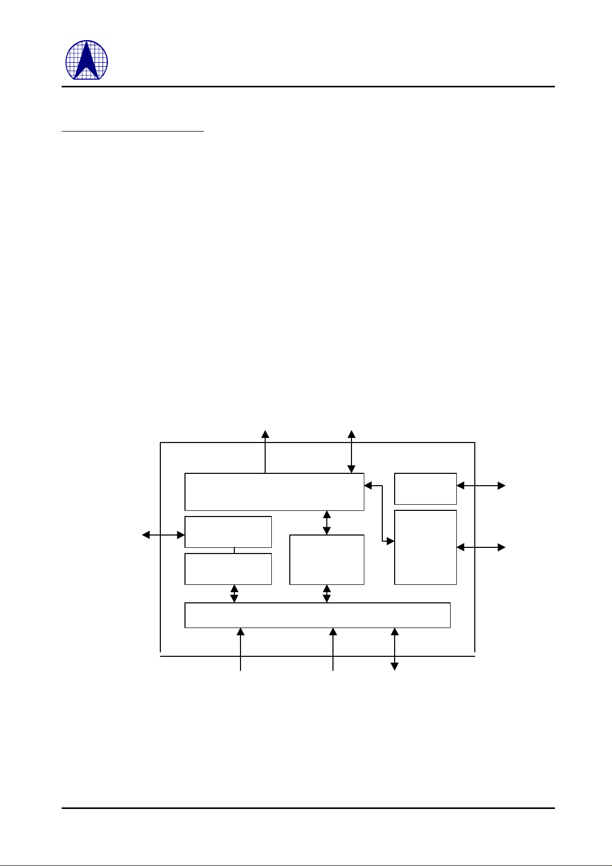
1.0 Introduction
Registers
I/F
SD[15:0]
SA[9:0]
Ctl BUS
MII I/F
MEMD[15:0]
MEMA[15:1]
EEDO
1.1 General Description:
The AX88195 provides industrial standard NE2000 registers level compatable instruction set. Various drivers
are easy acquired, maintenance and usage. No much additional effort to be paid. Software is easily port to
various embedded system with no pain and tears
The AX88195 Fast Ethernet Controller is a high performance local CPU bus Ethernet Controller. The AX88195
supports both 8 bit and 16 bit local CPU interfaces include MCS-51 series, 80x86 series, MC68K series CPU
and ISA bus. The AX88196 implements both 10Mbps and 100Mbps Ethernet function based on IEEE802.3 /
IEEE802.3u LAN standard and supports both 10Mbps/100Mbps media-independent interface (MII) to simplify
the design.
AX88195 use 128-pin LQFP low profile package, 25MHz operation, dual 5V and 3.3V CMOS process with 5V
I/O tolerance or pure 3.3V operation.
1.2 AX88195 Block Diagram:
EECS
EECK
EEDI
Fig - 1 AX88195 Block Diagram
SEEPROM
NE2000
SRAM
Arbiter
Remote
DMA
FIFOs
Host Interface
STA
MAC
Core
4
ASIX ELECTRONICS CORPORATION
Page 5

AX88195 Local CPU Bus Fast Ethernet MAC Controller
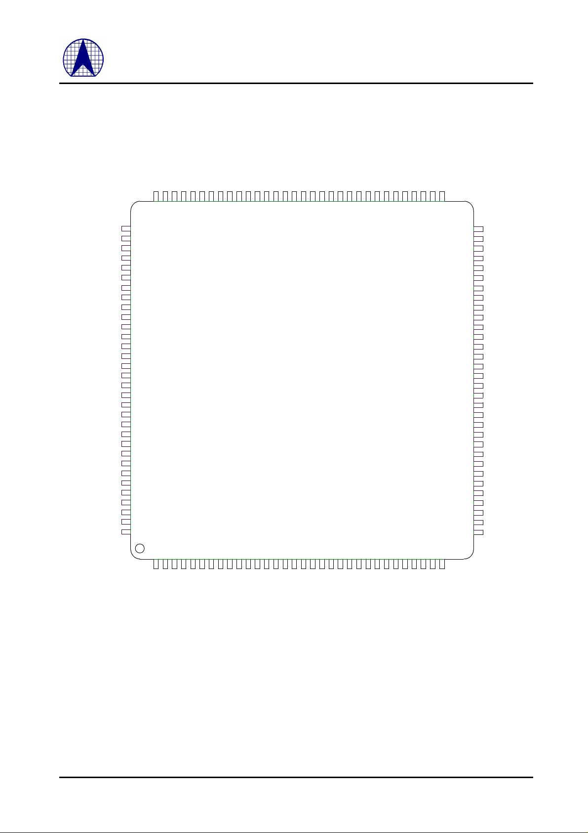
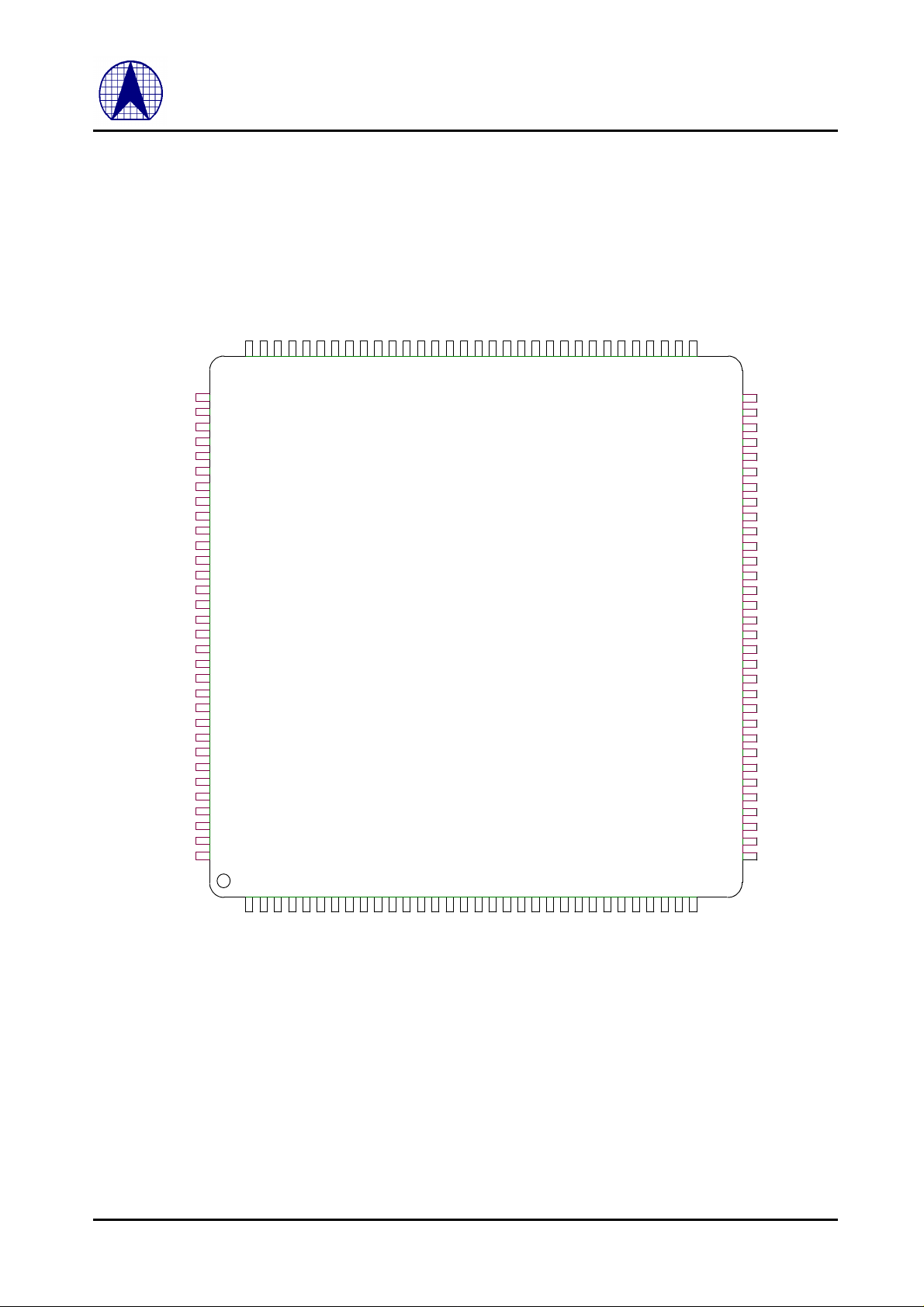
1.3 AX88195 Pin Connection Diagram
R/W
/LDS
/UDS
/IRQ
The AX88195 is housed in the 128-pin plastic light quad flat pack. Fig - 2 shows the AX88195 pin
connection diagram.
TX_EN
TXD[1]
TXD[2]
TXD[3]
LVDD
CLKO25M
VSS
LCLK/XTALIN
XTALOUT
VSS
EECS
EECK
EEDI
EEDO
LVDD
SAL[0]
SAL[1]
SAL[2]
SAH[0]
SAH[1]
SAH[2]
SAX[0]
SAX[1]
VSS
/IOCS16
SAX[2]
SAX[3]
/CS
AEN/PSEN
RDY/DTACK
/RESET
RESET
LVDD
97
98
99
100
101
102
103
104
105
106
107
108
109
110
111
112
113
114
115
116
117
118
119
120
121
122
123
124
125
126
127
128
TXD[0]
TX_CLK
96
95
94
VSS
93
MDC
MDIO
RXD[3]
RXD[2]
RXD[1]
90
8892858983
RXD[0]
CRS
RX_CLK
86
87
COL
84
AX88195
LOCAL CPU BUS
10/100BASE MAC
CONTROLLER
3
4
1
2
8
7
6
5
9
12
13
11
10
RX_DV
RX_ER
VSS
829181
16
15
14
MEMD[0]
MEMD[1]
MEMD[2]
MEMD[3]
78
77
797480
19
17
20
18
MEMD[4]
MEMD[5]
MEMD[6]
HVDD
75
73
76
24
21
23
22
MEMD[7]
MEMD[8]
MEMD[9]
VSS
71
72
70
69
26
25
28
27
MEMD[12]
MEMD[10]
MEMD[11]
MEMD[13]
66
65
68
67
32
31
29
30
64
63
62
61
60
59
58
57
56
55
54
53
52
51
50
49
48
47
46
45
44
43
42
41
40
39
38
37
36
35
34
33
HVDD
MEMD[14]
MEMD[15]
MEMA[1]
MEMA[2]
VSS
MEMA[3]
MEMA[4]
MEMA[5]
MEMA[6]
LVDD
MEMA[7]
MEMA[8]
MEMA[9]
MEMA[10]
VSS
MEMA[11]
MEMA[12]
MEMA[13]
MEMA[14]
LVDD
MEMA[15]
/MEMRD
/MEMWR
VSS
NC
SD[0]
SD[1]
SD[2]
SD[3]
VSS
SD[4]
NC
SA[1]
SA[0]
SA[3]
SA[2]
SA[5]
SA[4]
SA[6]
SA[7]
SA[9]
SA[8]
VSS
IRQ
NC
/IORD
/IOWR
NC
/BHE
HVDD
SD[14]
SD[13]
SD[15]
VSS
SD[12]
Fig - 2 AX88195 Pin Connection Diagram
5
ASIX ELECTRONICS CORPORATION
SD[9]
SD[11]
SD[10]
SD[8]
HVDD
SD[7]
SD[6]
SD[5]
Page 6
AX88195 Local CPU Bus Fast Ethernet MAC Controller
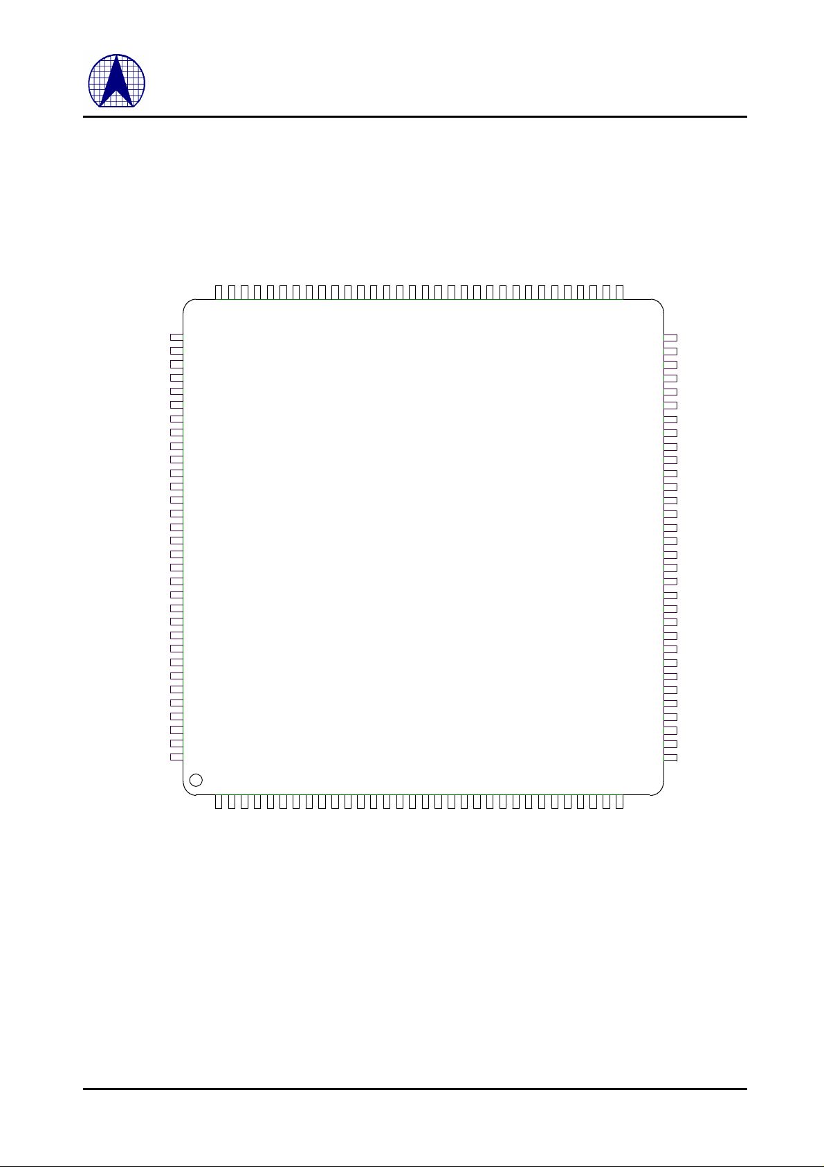
1.3.1 AX88195 Pin Connection Diagram for ISA Bus Mode
SA[1]
HVDD
HVDD
SA[0]
SA[3]
SA[2]
SA[5]
SA[4]
SA[6]
SA[7]
SA[9]
SA[8]
/IOWR
SD[15]
SD[14]
SD[13]
SD[12]
SD[11]
SD[10]
SD[9]
SD[8]
SD[6]
SD[5]
SD[7]
/BHE
/IORD
TX_EN
TXD[1]
TXD[2]
TXD[3]
LVDD
CLKO25M
VSS
LCLK/XTALIN
XTALOUT
VSS
EECS
EECK
EEDI
EEDO
LVDD
SAL[0]
SAL[1]
SAL[2]
SAH[0]
SAH[1]
SAH[2]
SAX[0]
SAX[1]
VSS
/IOCS16
SAX[2]
SAX[3]
/CS
AEN
RDY
/RESET
RESET
LVDD
97
98
99
100
101
102
103
104
105
106
107
108
109
110
111
112
113
114
115
116
117
118
119
120
121
122
123
124
125
126
127
128
TXD[0]
TX_CLK
96
95
94
VSS
93
MDC
MDIO
RXD[3]
RXD[2]
RXD[1]
90
8892858983
RXD[0]
CRS
RX_CLK
86
87
COL
84
AX88195
LOCAL CPU BUS
10/100BASE MAC
CONTROLLER
( for ISA Bus I/F )
RX_DV
RX_ER
VSS
829181
MEMD[0]
MEMD[1]
MEMD[2]
MEMD[3]
78
77
797480
MEMD[4]
MEMD[5]
MEMD[6]
HVDD
75
73
76
MEMD[7]
MEMD[8]
71
72
MEMD[9]
MEMD[10]
MEMD[11]
VSS
70
68
67
69
MEMD[12]
MEMD[13]
66
65
64
63
62
61
60
59
58
57
56
55
54
53
52
51
50
49
48
47
46
45
44
43
42
41
40
39
38
37
36
35
34
33
HVDD
MEMD[14]
MEMD[15]
MEMA[1]
MEMA[2]
VSS
MEMA[3]
MEMA[4]
MEMA[5]
MEMA[6]
LVDD
MEMA[7]
MEMA[8]
MEMA[9]
MEMA[10]
VSS
MEMA[11]
MEMA[12]
MEMA[13]
MEMA[14]
LVDD
MEMA[15]
/MEMRD
/MEMWR
VSS
NC
SD[0]
SD[1]
SD[2]
SD[3]
VSS
SD[4]
3
4
1
2
Fig - 3 AX88195 Pin Connection Diagram for ISA Bus Mode
8
7
6
5
9
10
11
VSS
IRQ
12
13
NC
15
14
6
16
17
NC
NC
19
18
24
21
23
22
20
VSS
ASIX ELECTRONICS CORPORATION
26
25
27
28
29
30
31
32
Page 7
AX88195 Local CPU Bus Fast Ethernet MAC Controller
1.3.2 AX88195 Pin Connection Diagram for 80x86 Mode
SA[1]
HVDD
HVDD
SA[0]
SA[3]
SA[2]
SA[5]
SA[4]
SA[6]
SA[7]
SA[9]
SA[8]
/IOWR
SD[15]
SD[14]
SD[13]
SD[12]
SD[11]
SD[10]
SD[9]
SD[8]
SD[6]
SD[5]
SD[7]
/BHE
/IORD
TX_EN
TXD[1]
TXD[2]
TXD[3]
LVDD
CLKO25M
VSS
LCLK/XTALIN
XTALOUT
VSS
EECS
EECK
EEDI
EEDO
LVDD
SAL[0]
SAL[1]
SAL[2]
SAH[0]
SAH[1]
SAH[2]
SAX[0]
SAX[1]
VSS
NC
SAX[2]
SAX[3]
/CS
NC
RDY
/RESET
RESET
LVDD
97
98
99
100
101
102
103
104
105
106
107
108
109
110
111
112
113
114
115
116
117
118
119
120
121
122
123
124
125
126
127
128
TXD[0]
TX_CLK
96
95
94
VSS
93
MDC
MDIO
RXD[3]
RXD[2]
RXD[1]
90
8892858983
RXD[0]
CRS
RX_CLK
86
87
COL
84
AX88195
LOCAL CPU BUS
10/100BASE MAC
CONTROLLER
(for x86 Interface)
RX_DV
RX_ER
VSS
829181
MEMD[0]
MEMD[1]
MEMD[2]
MEMD[3]
78
77
797480
MEMD[4]
MEMD[5]
MEMD[6]
HVDD
75
73
76
MEMD[7]
72
MEMD[8]
MEMD[9]
MEMD[10]
VSS
71
70
68
69
MEMD[12]
MEMD[11]
MEMD[13]
66
65
67
64
63
62
61
60
59
58
57
56
55
54
53
52
51
50
49
48
47
46
45
44
43
42
41
40
39
38
37
36
35
34
33
HVDD
MEMD[14]
MEMD[15]
MEMA[1]
MEMA[2]
VSS
MEMA[3]
MEMA[4]
MEMA[5]
MEMA[6]
LVDD
MEMA[7]
MEMA[8]
MEMA[9]
MEMA[10]
VSS
MEMA[11]
MEMA[12]
MEMA[13]
MEMA[14]
LVDD
MEMA[15]
/MEMRD
/MEMWR
VSS
NC
SD[0]
SD[1]
SD[2]
SD[3]
VSS
SD[4]
3
4
1
2
Fig - 4 AX88195 Pin Connection Diagram for 80x86 Mode
8
7
6
5
9
10
11
VSS
IRQ
12
13
NC
15
14
7
16
17
NC
NC
19
18
24
21
23
22
20
VSS
ASIX ELECTRONICS CORPORATION
26
25
27
28
29
30
31
32
Page 8
AX88195 Local CPU Bus Fast Ethernet MAC Controller
1.3.3 AX88195 Pin Connection Diagram for MC68K Mode
SA[1]
HVDD
HVDD
SA[3]
SA[2]
SA[5]
SA[4]
SA[6]
SA[7]
SA[9]
SA[8]
SD[15]
SD[14]
SD[13]
SD[12]
SD[11]
SD[10]
SD[9]
SD[8]
SD[6]
SD[5]
SD[7]
/LDS
/UDS
/IRQ
TX_EN
TXD[1]
TXD[2]
TXD[3]
LVDD
CLKO25M
VSS
LCLK/XTALIN
XTALOUT
VSS
EECS
EECK
EEDI
EEDO
LVDD
SAL[0]
SAL[1]
SAL[2]
SAH[0]
SAH[1]
SAH[2]
SAX[0]
SAX[1]
VSS
NC
SAX[2]
SAX[3]
/CS
NC
/DTACK
/RESET
RESET
LVDD
97
98
99
100
101
102
103
104
105
106
107
108
109
110
111
112
113
114
115
116
117
118
119
120
121
122
123
124
125
126
127
128
TXD[0]
TX_CLK
96
95
94
VSS
93
MDC
MDIO
RXD[3]
RXD[2]
RXD[1]
90
8892858983
RXD[0]
CRS
RX_CLK
86
87
COL
84
AX88195
LOCAL CPU BUS
10/100BASE MAC
CONTROLLER
(for 68K Interface)
3
4
1
2
8
7
6
5
9
12
13
11
10
RX_DV
RX_ER
VSS
829181
16
15
14
MEMD[0]
MEMD[1]
MEMD[2]
MEMD[3]
78
77
797480
19
17
20
18
MEMD[4]
MEMD[5]
MEMD[6]
HVDD
75
73
76
24
21
23
22
MEMD[7]
MEMD[8]
71
72
26
25
MEMD[9]
MEMD[10]
MEMD[11]
VSS
70
68
67
69
28
29
27
30
MEMD[12]
MEMD[13]
66
65
64
63
62
61
60
59
58
57
56
55
54
53
52
51
50
49
48
47
46
45
44
43
42
41
40
39
38
37
36
35
34
33
32
31
HVDD
MEMD[14]
MEMD[15]
MEMA[1]
MEMA[2]
VSS
MEMA[3]
MEMA[4]
MEMA[5]
MEMA[6]
LVDD
MEMA[7]
MEMA[8]
MEMA[9]
MEMA[10]
VSS
MEMA[11]
MEMA[12]
MEMA[13]
MEMA[14]
LVDD
MEMA[15]
/MEMRD
/MEMWR
VSS
NC
SD[0]
SD[1]
SD[2]
SD[3]
VSS
SD[4]
NC
NC
R/W
NC
VSS
VSS
NC
Fig - 5 AX88195 Pin Connection Diagram for MC68K Mode
8
ASIX ELECTRONICS CORPORATION
Page 9
AX88195 Local CPU Bus Fast Ethernet MAC Controller
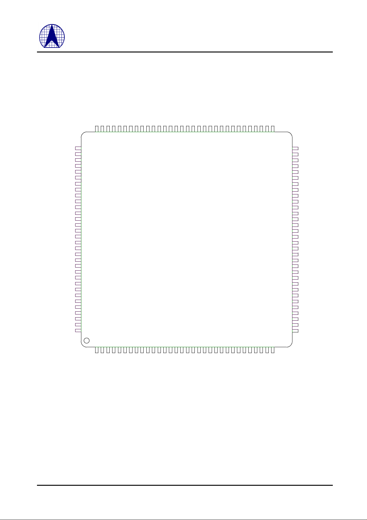
1.3.4 AX88195 Pin Connection Diagram for MCS-51 Mode
SA[1]
VSS
HVDD
HVDD
SA[0]
SA[3]
SA[2]
SA[5]
SA[4]
SA[6]
SA[7]
SA[9]
SA[8]
/IOWR
SD[6]
SD[5]
SD[7]
/IORD
/IRQ
TX_EN
TXD[1]
TXD[2]
TXD[3]
LVDD
CLKO25M
VSS
LCLK/XTALIN
XTALOUT
VSS
EECS
EECK
EEDI
EEDO
LVDD
SAL[0]
SAL[1]
SAL[2]
SAH[0]
SAH[1]
SAH[2]
SAX[0]
SAX[1]
VSS
NC
SAX[2]
SAX[3]
/CS
/PSEN
NC
/RESET
RESET
LVDD
97
98
99
100
101
102
103
104
105
106
107
108
109
110
111
112
113
114
115
116
117
118
119
120
121
122
123
124
125
126
127
128
TXD[0]
TX_CLK
96
95
94
VSS
93
MDC
MDIO
RXD[3]
RXD[2]
RXD[1]
90
8892858983
RXD[0]
CRS
RX_CLK
86
87
COL
84
AX88195
LOCAL CPU BUS
10/100BASE MAC
CONTROLLER
(for 8051 Interface)
3
4
1
2
8
7
6
5
9
12
13
11
10
RX_DV
RX_ER
VSS
829181
16
15
14
MEMD[0]
MEMD[1]
MEMD[2]
MEMD[3]
78
77
797480
19
17
20
18
MEMD[4]
MEMD[5]
MEMD[6]
HVDD
75
73
76
24
21
23
22
MEMD[7]
MEMD[8]
MEMD[9]
71
72
70
26
25
MEMD[10]
VSS
68
69
28
29
27
MEMD[12]
MEMD[11]
MEMD[13]
66
65
67
64
63
62
61
60
59
58
57
56
55
54
53
52
51
50
49
48
47
46
45
44
43
42
41
40
39
38
37
36
35
34
33
32
31
30
HVDD
MEMD[14]
MEMD[15]
MEMA[1]
MEMA[2]
VSS
MEMA[3]
MEMA[4]
MEMA[5]
MEMA[6]
LVDD
MEMA[7]
MEMA[8]
MEMA[9]
MEMA[10]
VSS
MEMA[11]
MEMA[12]
MEMA[13]
MEMA[14]
LVDD
MEMA[15]
/MEMRD
/MEMWR
VSS
NC
SD[0]
SD[1]
SD[2]
SD[3]
VSS
SD[4]
VSS
NC
NC
NC
NC
NCNCNC
NC
NC
Fig - 6 AX88195 Pin Connection Diagram for MCS-51 Mode
9
ASIX ELECTRONICS CORPORATION
NCNCNC
Page 10

AX88195 Local CPU Bus Fast Ethernet MAC Controller
2.0 Signal Description
The following terms describe the AX88195 pin-out:
All pin names with the “/” suffix are asserted low.
The following abbreviations are used in following Tables.
I Input PU Pull Up
O Output PD Pull Down
I/O Input/Output P Power Pin
OD Open Drain
2.1 Local CPU Bus Interface Signals Group
SIGNAL TYPE PIN NO. DESCRIPTION
SAL[2:0] I/PD 113 – 111 System Address Select Low : Signals SAL[2:0] are additional address
signal input lines which active low enable higher I/O address decoder
on chip.
SAH[2:0] I/PU 116 – 114 System Address Select High : Signals SAH[2:0] are additional
address signal input lines which active high enable higher I/O
address decoder on chip.
SAX[3:0] I/PU 122 – 121
118 – 117
SA[9:1],
SA[0]/UDS
/BHE
or
/LDS
SD[15:0] I/O 20 – 23,
IREQ/IREQ O 12 Interrupt Request : When ISA BUS or 80186 CPU mode is select.
RDY/DTACK OD 125 Ready : This signal is set low to insert wait states during Remote
/CS I 123 Chip Select
/IORD I 15 I/O Read :The host asserts /IORD to read data from AX88195 I/O
/IOWR
or
R/W
I 10 – 1 System Address : Signals SA[9:0] are address bus input lines which
I 18 Bus High Enable or Lower Data Strobe : Bus High Enable is active
25 – 28,
30 – 33,
35 – 38
I 14 I/O Write :The host asserts /IOWR to write data into AX88195 I/O
System Address Select Low/High : Signals SAX[3:0] are additional
address signal input lines which active low/high depend on power on
setting to enable higher I/O address decoder on chip.
lower I/O spaces on chip. SA[0] also means Upper Data Strobe
(/UDS) active low signal in 68K application mode.
low signal in some 16 bit application mode which enable high bus
(SD[15:8]) active. The signal also name as Lower Data Strobe (/LDS)
for 68K application mode.
System Data Bus : Signals SD[15:0] constitute the bi-directional
data bus.
IREQ is asserted high to indicate the host system that the chip
requires host software service. When MC68K or MCS-51 CPU
mode is select. /IREQ is asserted low to indicate the host system that
the chip requires host software service.
DMA transfer.
/Dtack : When Motorola CPU type is select, the pin is active low
inform CPU that data is accepted.
When the /CS signal is asserted, the chip is selected.
space. When Motorola CPU type is select , the pin is useless.
space. When Motorola CPU type is select, the pin is active high for
read operation at the same time.
10
ASIX ELECTRONICS CORPORATION
Page 11

AX88195 Local CPU Bus Fast Ethernet MAC Controller
/IOCS16 OD 120 I/O is 16 Bit Port : The /IOIS16 is asserted when the address at the
range corresponds to an I/O address to which the chip responds, and
the I/O port addressed is capable of 16-bit access.
AEN
or
/PSEN
Tab - 1 Local CPU bus interface signals group
I/PD 124 Address Enable : The signal is asserted when the address bus is
available for DMA cycle. When negated (low), AX88195 an I/O slave
device may respond to addresses and I/O command.
PSEN : This signal is active low for 8051 program access. For I/O
device, AX88195, this signal is active high to access the chip. This
signal is for 8051 bus application only.
2.2 MII interface signals group
SIGNAL TYPE PIN NO. DESCRIPTION
RXD[3:0] I 90 – 87 Receive Data : RXD[3:0] is driven by the PHY synchronously with
respect to RX_CLK.
CRS I 85 Carrier Sense : Asynchronous signal CRS is asserted by the PHY
when either the transmit or receive medium is non-idle.
RX_DV I 83 Receive Data Valid : RX_DV is driven by the PHY synchronously
with respect to RX_CLK. Asserted high when valid data is present on
RXD [3:0].
RX_ER I 82 Receive Error : RX_ER ,is driven by PHY and synchronous to
RX_CLK, is asserted for one or more RX_CLK periods to indicate to
the port that an error has detected.
RX_CLK I 86 Receive Clock : RX_CLK is a continuous clock that provides the
timing reference for the transfer of the RX_DV,RXD[3:0] and
RX_ER signals from the PHY to the MII port of the repeater.
COL I 84 Collision : this signal is driven by PHY when collision is detected.
TX_EN O 95 Transmit Enable : TX_EN is transition synchronously with respect to
the rising edge of TX_CLK. TX_EN indicates that the port is
presenting nibbles on TXD [3:0] for transmission.
TXD[3:0] O 99 – 96 Transmit Data : TXD[3:0] is transition synchronously with respect to
the rising edge of TX_CLK. For each TX_CLK period in which
TX_EN is asserted, TXD[3:0] are accepted for transmission by the
PHY.
TX_CLK I 94 Transmit Clock : TX_CLK is a continuous clock from PHY. It
provides the timing reference for the transfer of the TX_EN and
TXD[3:0] signals from the MII port to the PHY.
MDC O 92 Station Management Data Clock : The timing reference for MDIO.
All data transfers on MDIO are synchronized to the rising edge of this
clock. MDC is a 2.5MHz frequency clock output.
MDIO I/O/PU 91 Station Management Data Input / Output : Serial data input/output
transfers from/to the PHYs . The transfer protocol conforms to the
IEEE 802.3u MII specification.
Tab - 2 MII interface signals group
11
ASIX ELECTRONICS CORPORATION
Page 12

AX88195 Local CPU Bus Fast Ethernet MAC Controller
2.3 EEPROM Signals Group
SIGNAL TYPE PIN NO. DESCRIPTION
EECS O 106 EEPROM Chip Select : EEPROM chip select signal.
EECK O 107 EEPROM Clock : Signal connected to EEPROM clock pin.
EEDI O 108 EEPROM Data In : Signal connected to EEPROM data input pin.
EEDO I/PU 109 EEPROM Data Out : Signal connected to EEPROM data output pin.
Tab - 3 EEPROM bus interface signals group
2.4 SRAM Interface pins group
SIGNAL TYPE PIN NO. DESCRIPTION
MEMA[15:1] O 43, 45 – 48,
50 –53’
55 – 58,
60 – 61
MEMD[15:0] I/O/PU 62 – 63,
65 – 68,
70 – 74,
76 – 80
/MEMRD O 42 SRAM Read
/MEMWR O 41 SRAM Write
SRAM Address :
SRAM Data :
Tab - 4 SRAM Interface pins group
2.5 Miscellaneous pins group
SIGNAL TYPE PIN NO. DESCRIPTION
LCLK/XTALIN I 103 CMOS Local Clock : A 25Mhz clock, +/- 100 ppm, 40%-60% duty
cycle.
Crystal Oscillator Input : A 25Mhz crystal, +/- 25 ppm can be
connected across XTALIN and XTALOUT.
XTALOUT O 104 Crystal Oscillator Output : A 25Mhz crystal, +/- 25 ppm can be
connected across XTALIN and XTALOUT. If a single-ended external
clock (LCLK) is connected to XTALIN, the crystal output pin should
be left floating.
CLKO25M O 101 Clock Output 25MHz : This clock is source from LCLK/XTALIN.
RESET I/PD 127 Reset
Reset is active high then place AX88195 into reset mode immediately.
During Falling edge the AX88195 loads the power on setting data.
User can select either RESET or /RESET for applications.
/RESET I/PU 126 /Reset
Reset is active low then place AX88195 into reset mode immediately.
During rising edge the AX88195 loads the power on setting data.
User can select either RESET or /RESET for applications.
NC N/A 13, 16, 17,39No Connection : for manufacturing test only.
LVDD P 44, 54,
100, 110,
128
Power Supply : +3.3V DC.
12
ASIX ELECTRONICS CORPORATION
Page 13

AX88195 Local CPU Bus Fast Ethernet MAC Controller
HVDD P 19, 29, 64,75Power Supply : +5V DC.
Note : for pure 3.3V single power solution, all the HVDD pin can
connect to +3.3V. Care should be taken that HVDD input power must
be greater or equal ( > = ) than LVDD.
VSS P 11, 24, 34,
40, 49,59,
69, 81,93,
102, 105,
119
Tab - 5 Miscellaneous pins group
Power Supply : +0V DC or Ground Power.
2.6 Power on configuration setup signals cross reference table
SIGNAL NAME SHARE WITH DESCRIPTION
IO_BASE[2:0] MEMD[15:13] IO_BASE[2] IO_BASE[1] IO_BASE[0] IO_BASE
0 0 0 300h
0 0 1 320h
0 1 0 340h
0 1 1 360h
1 0 0 380h
1 0 1 3A0h
1 1 0 200h
1 1 1 220h
SAX[3:0] MEMD[12:9] SAX[3] address decode depends on MEMD[12] power on value
SAX[2] address decode depends on MEMD[11] power on value
SAX[1] address decode depends on MEMD[10] power on value
SAX[0] address decode depends on MEMD[9] power on value
CPU TYPE MEMD[8:7] MEMD[8] MEMD[7] CPU TYPE
0 0 ISA BUS
0 1 80186
1 0 MC68K
1 1 MCS-51 (805X)
All of the above signals are pull-up for default values.
Tab - 6 Power on Configuration Setup Table
13
ASIX ELECTRONICS CORPORATION
Page 14

AX88195 Local CPU Bus Fast Ethernet MAC Controller
3.0 Memory and I/O Mapping
There are four memory or I/O mapping used in AX88195.
1. EEPROM Memory Mapping
2. I/O Mapping
3. Local Memory Mapping
3.1 EEPROM Memory Mapping
User can define by themselves and can access via I/O address offset 14H MII/EEPROM registers
3.2 I/O Mapping
SYSTEM I/O OFFSET FUNCTION
0000H
001FH
Tab - 7 I/O Address Mapping
MAC CORE REGISTER
3.3 SRAM Memory Mapping
OFFSET FUNCTION
4000H
7FFF
0000H
FFFFH
Tab - 8 Local Memory Mapping
NE2000 COMPATABLE MODE
8K X 16 SRAM BUFFER
EXTENSION MODE
32K X 16 SRAM BUFFER
14
ASIX ELECTRONICS CORPORATION
Page 15

AX88195 Local CPU Bus Fast Ethernet MAC Controller
4.0 Registers Operation
All registers of MAC Core are 8-bit wide and mapped into pages which are selected by PS in the Command
Register.
PAGE 0 (PS1=0,PS0=0)
OFFSET READ WRITE
00H Command Register
( CR )
01H Page Start Register
( PSTART )
02H Page Stop Register
( PSTOP )
03H Boundary Pointer
( BNRY )
04H Transmit Status Register
( TSR )
05H Number of Collisions Register
( NCR )
06H Current Page Register
( CPR )
07H Interrupt Status Register
( ISR )
08H Current Remote DMA Address 0
( CRDA0 )
09H Current Remote DMA Address 1
( CRDA1 )
0AH Reserved Remote Byte Count 0
0BH Reserved Remote Byte Count 1
0CH Receive Status Register
( RSR )
0DH Frame Alignment Errors
( CNTR0 )
0EH CRC Errors
( CNTR1 )
0FH Missed Packet Errors
( CNTR2 )
10H
11H
12H IFGS1 IFGS1
13H IFGS2 IFGS2
14H MII/EEPROM Access MII/EEPROM Access
15H - Test Register
16H Inter-frame Gap (IFG) Inter-frame Gap (IFG)
17H
to
1EH
1FH Reset Reserved
Data Port Data Port
Reserved Reserved
Command Register
( CR )
Page Start Register
( PSTART )
Page Stop Register
( PSTOP )
Boundary Pointer
( BNRY )
Transmit Page Start Address
( TPSR )
Transmit Byte Count Register 0
( TBCR0 )
Transmit Byte Count Register 1
( TBCR1 )
Interrupt Status Register
( ISR )
Remote Start Address Register 0
( RSAR0 )
Remote Start Address Register 1
( RSAR1 )
( RBCR0 )
( RBCR1 0
Receive Configuration Register
( RCR )
Transmit Configuration Register ( TCR )
Data Configuration Register
( DCR )
Interrupt Mask Register
( IMR )
Tab - 9 Page 0 of MAC Core Registers Mapping
15
ASIX ELECTRONICS CORPORATION
Page 16

AX88195 Local CPU Bus Fast Ethernet MAC Controller
PAGE 1 (PS1=0,PS0=1)
OFFSET READ WRITE
00H Command Register
( CR )
01H Physical Address Register 0
( PARA0 )
02H Physical Address Register 1
( PARA1 )
03H Physical Address Register 2
( PARA2 )
04H Physical Address Register 3
( PARA3 )
05H Physical Address Register 4
( PARA4 )
06H Physical Address Register 5
( PARA5 )
07H Current Page Register
( CPR )
08H Multicast Address Register 0
( MAR0 )
09H Multicast Address Register 1
( MAR1 )
0AH Multicast Address Register 2
( MAR2 )
0BH Multicast Address Register 3
( MAR3 )
0CH Multicast Address Register 4
( MAR4 )
0DH Multicast Address Register 5
( MAR5 )
0EH Multicast Address Register 6
( MAR6 )
0FH Multicast Address Register 7
( MAR7 )
10H
11H
12H Inter-frame Gap Segment 1
13H Inter-frame Gap Segment 2
14H MII/EEPROM Access MII/EEPROM Access
15H - Test Register
16H Inter-frame Gap (IFG) Inter-frame Gap (IFG)
17H
to
1EH
1FH Reset Reserved
Data Port Data Port
IFGS1
IFGS2
Reserved Reserved
Command Register
( CR )
Physical Address Register 0
( PAR0 )
Physical Address Register 1
( PAR1 )
Physical Address Register 2
( PAR2 )
Physical Address Register 3
( PAR3 )
Physical Address Register 4
( PAR4 )
Physical Address Register 5
( PAR5 )
Current Page Register
( CPR )
Multicast Address Register 0
( MAR0 )
Multicast Address Register 1
( MAR1 )
Multicast Address Register 2
( MAR2 )
Multicast Address Register 3
( MAR3 )
Multicast Address Register 4
( MAR4 )
Multicast Address Register 5
( MAR5 )
Multicast Address Register 6
( MAR6 )
Multicast Address Register 7
( MAR7 )
Inter-frame Gap Segment 1
IFGS1
Inter-frame Gap Segment 2
IFGS2
Tab - 10 Page 1 of MAC Core Registers Mapping
16
ASIX ELECTRONICS CORPORATION
Page 17

AX88195 Local CPU Bus Fast Ethernet MAC Controller
4.1 Command Register (CR) Offset 00H (Read/Write)
FIELD NAME DESCRIPTION
7:6 PS1,PS0 PS1,PS0 : Page Select
The two bit selects which register page is to be accessed.
PS1 PS0
0 0 page 0
0 1 page 1
5:3 RD2,RD1
,RD0
2 TXP TXP : Transmit Packet
1 START START :
0 STOP STOP : Stop AX88195
RD2,RD1,RD0 : Remote DMA Command
These three encoded bits control operation of the Remote DMA channel. RD2 could be set
to abort any Remote DMA command in process. RD2 is reset by AX88195 when a Remote
DMA has been completed. The Remote Byte Count should be cleared when a Remote DMA
has been aborted. The Remote Start Address are not restored to the starting address if the
Remote DMA is aborted.
RD2 RD1 RD0
0 0 0 Not allowed
0 0 1 Remote Read
0 1 0 Remote Write
0 1 1 Not allowed
1 X X Abort / Complete Remote DMA
This bit could be set to initiate transmission of a packet
This bit is used to active AX88195 operation.
This bit is used to stop the AX88195 operation.
4.2 Interrupt Status Register (ISR) Offset 07H (Read/Write)
FIELD NAME DESCRIPTION
7 RST Reset Status :
Set when AX88195 enters reset state and cleared when a start command is issued to the
CR. Writing to this bit is no effect.
6 RDC Remote DMA Complete
Set when remote DMA operation has been completed
5 CNT Counter Overflow
Set when MSB of one or more of the Tally Counters has been set.
4 OVW OVERWRITE : Set when receive buffer ring storage resources have been exhausted.
3 TXE Transmit Error
Set when packet transmitted with one or more of the following errors
n Excessive collisions
n FIFO Underrun
2 RXE Receive Error
Indicates that a packet was received with one or more of the following errors
CRC error
Frame Alignment Error
FIFO Overrun
Missed Packet
1 PTX Packet Transmitted
Indicates packet transmitted with no error
0 PRX Packet Received
Indicates packet received with no error.
17
ASIX ELECTRONICS CORPORATION
Page 18

AX88195 Local CPU Bus Fast Ethernet MAC Controller
4.3 Interrupt mask register (IMR) Offset 0FH (Write)
FIELD NAME DESCRIPTION
7 - Reserved
6 RDCE DMA Complete Interrupt Enable. Default “low” disabled.
5 CNTE Counter Overflow Interrupt Enable. Default “low” disabled.
4 OVWE Overwrite Interrupt Enable. Default “low” disabled.
3 TXEE Transmit Error Interrupt Enable. Default “low” disabled.
2 RXEE Receive Error Interrupt Enable. Default “low” disabled.
1 PTXE Packet Transmitted Interrupt Enable. Default “low” disabled.
0 PRXE Packet Received Interrupt Enable. Default “low” disabled.
4.4 Data Configuration Register (DCR) Offset 0EH (Write)
FIELD NAME DESCRIPTION
7 RDCR Remote DMA always completed
6:2 - Reserved
1 BOS Byte Order Select
0: MS byte placed on AD15:AD8 and LS byte on AD7-AD0 (80186).
1: MS byte placed on AD7::AD0 and LS byte on AD15:AD0(MC68K)
0 WTS Word Transfer Select
0 : Selects byte-wide DMA transfers.
1 : Selects word-wide DMA transfers.
4.5 Transmit Configuration Register (TCR) Offset 0DH (Write)
FIELD NAME DESCRIPTION
7 FDU Full Duplex :
This bit indicates the current media mode is Full Duplex or not.
0 : Half duplex
1 : Full duplex
6 PD Pad Disable
0 : Pad will be added when packet length less than 60.
1 : Pad will not be added when packet length less than 60.
5 RLO Retry of late collision
0 : Don’t retransmit packet when late collision happens.
1 : Retransmit packet when late collision happens.
4:3 - Reserved
2:1 LB1,LB0 Encoded Loop-back Control
These encoded configuration bits set the type of loop-back that is to be performed.
LB1 LB0
Mode 0 0 0 Normal operation
Mode 1 0 1 Internel NIC loop-back
Mode 2 1 0 PHYcevisor loop-back
0 CRC Inhibit CRC
0 : CRC appended by transmitter.
1 : CRC inhibited by transmitter.
18
ASIX ELECTRONICS CORPORATION
Page 19

AX88195 Local CPU Bus Fast Ethernet MAC Controller
4.6 Transmit Status Register (TSR) Offset 04H (Read)
FIELD NAME DESCRIPTION
7 OWC Out of window collision
6:4 - Reserved
3 ABT Transmit Aborted
Indicates the AX88195 aborted transmission because of excessive collision.
2 COL Transmit Collided
Indicates that the transmission collided at least once with another station on the network.
1 - Reserved
0 PTX Packet Transmitted
Indicates transmission without error.
4.7 Receive Configuration (RCR) Offset 0CH (Write)
FIELD NAME DESCRIPTION
7 - Reserved
6 INTT Interrupt Trigger Mode for ISA and 80186 modes
0 : Low active
1 : High active (default)
Interrupt Trigger Mode for MCS-51 and MC68K modes
0 : High active
1 : Low active (default)
5 MON Monitor Mode
0 : Normal Operation
1 : Monitor Mode, the input packet will be checked on NODE ADDRESS and CRC but not
buffered into memory.
4 PRO PRO : Promiscuous Mode
Enable the receiver to accept all packets with a physical address.
3 AM AM : Accept Multicast
Enable the receiver to accept packets with a multicast address. That multicast address must
pass the hashing array.
2 AB AB : Accept Broadcast
Enable the receiver to accept broadcast packet.
1 AR AR : Accept Runt
Enable the receiver to accept runt packet.
0 SEP SEP : Save Error Packet
Enable the receiver to accept and save packets with error.
4.8 Receive Status Register (RSR) Offset 0CH (Read)
FIELD NAME DESCRIPTION
7 - Reserved
6 DIS Receiver Disabled
5 PHY Multicast Address Received.
4 MPA Missed Packet
3 FO FIFO Overrun
2 FAE Frame alignment error.
1 CR CRC error.
0 PRX Packet Received Intact
19
ASIX ELECTRONICS CORPORATION
Page 20

AX88195 Local CPU Bus Fast Ethernet MAC Controller
4.9 Inter-frame gap (IFG) Offset 16H (Read/Write)
FIELD NAME DESCRIPTION
7 - Reserved
6:0 IFG Inter-frame Gap. Default value 15H.
4.10 Inter-frame gap Segment 1(IFGS1) Offset 12H (Read/Write)
FIELD NAME DESCRIPTION
7 - Reserved
6:0 IFG Inter-frame Gap Segment 1. Default value 0cH.
4.11 Inter-frame gap Segment 2(IFGS2) Offset 13H (Read/Write)
FIELD NAME DESCRIPTION
7 - Reserved
6:0 IFG Inter-frame Gap Segment 2. Default value 11H.
4.12 MII/EEPROM Management Register (MEMR) Offset 14H (Read/Write)
FIELD NAME DESCRIPTION
7 EECLK EECLK:
EEPROM Clock
6 EEO EEO : (Read only)
EEPROM Data Out value. That reflects Pin-109 EEDO value.
5 EEI EEI
EEPROM Data In. That output to Pin-108 EEDI as EEPROM data input value.
4 EECS EECS
EEPROM Chip Select
3 MDO MDO
MII Data Out
2 MDI MDI: (Read only)
MII Data In. That reflects Pin-91 MDIO value.
1 MDIR MII STA MDIO signal Direction
MII Read Control Bit, assert this bit let MDIO signal as the input signal. Deassert this bit
let MDIO as output signal.
0 MDC MDC
MII Clock
4.13 Test Register (TR) Offset 15H (Write)
FIELD NAME DESCRIPTION
7:5 - Reserved
4 TF16T Test for Collision
3 TPE Test pin Enable
2:0 IFG Select Test Pins Output
20
ASIX ELECTRONICS CORPORATION
Page 21

AX88195 Local CPU Bus Fast Ethernet MAC Controller
5.0 CPU I/O Read and Write Functions
The AX88195 supports four kinds of CPU/BUS types access function, including ISA, 80186,
MC68000 and MCS-51. These Access methods are described as the following sections.
5.1 ISA bus type access functions.
ISA bus I/O Read function
Function Mode /CS /BHE A0 /IORD /IOWR SD[15:8] SD[7:0]
Standby Mode H X X X X High-Z High-Z
Byte Access L
L
Word Access L L L L H Odd-Byte Even-Byte
ISA bus I/O Write function
Function Mode /CS /BHE A0 /IORD /IOWR SD[15:8] SD[7:0]
Standby Mode H X X X X X X
Byte Access L
L
Word Access L L L H L Odd-Byte Even-Byte
5.2 80186 CPU bus type access functions.
H
H
H
H
L
H
L
H
L
L
H
H
H
H
L
L
Not Valid
Not Valid
X
X
Even-Byte
Odd-Byte
Even-Byte
Odd-Byte
80186 CPU bus I/O Read function
Function Mode /CS /BHE A0 /IORD /IOWR SD[15:8] SD[7:0]
Standby Mode H X X X X High-Z High-Z
Byte Access L
L
Word Access L L L L H Odd-Byte Even-Byte
80186 CPU bus I/O Write function
Function Mode /CS /BHE A0 /IORD /IOWR SD[15:8] SD[7:0]
Standby Mode H X X X X X X
Byte Access L
L
Word Access L L L H L Odd-Byte Even-Byte
H
L
H
L
L
H
L
H
L
L
H
H
H
H
L
L
Not Valid
Odd-Byte
X
Odd-Byte
Even-Byte
Not Valid
Even-Byte
X
21
ASIX ELECTRONICS CORPORATION
Page 22

AX88195 Local CPU Bus Fast Ethernet MAC Controller
5.3 MC68K CPU bus type access functions.
68K bus I/O Read function
Function Mode /CS /UDS /LDS R/W SD[15:8] SD[7:0]
Standby Mode H X X X High-Z High-Z
Byte Access L
L
Word Access L L L H Even-Byte Odd-Byte
68K bus I/O Write function
Function Mode /CS /UDS /LDS R/W SD[15:8] SD[7:0]
Standby Mode H X X X X X
Byte Access L
L
Word Access L L L L Even-Byte Odd-Byte
H
L
H
L
L
H
L
H
H
H
L
L
Not Valid
Even-Byte
X
Even-Byte
Odd-Byte
Not Valid
Odd-Byte
X
5.3 MCS-51 CPU bus type access functions.
8051 bus I/O Read function
Function Mode /CS /PSEN SA0 /IORD /IOWR SD[15:8] SD[7:0]
Standby Mode H
X
Byte Access L
L
X
L
H
H
X
X
L
H
X
X
L
L
X
X
H
H
High-Z
High-Z
Not Valid
Not Valid
High-Z
High-Z
Even-Byte
Odd-Byte
8051 bus I/O Write function
Function Mode /CS /PSEN SA0 /IORD /IOWR SD[15:8] SD[7:0]
Standby Mode H
X
Byte Access L
L
X
L
H
H
X
X
L
H
X
X
H
H
X
X
L
L
X
X
X
X
X
X
Even-Byte
Odd-Byte
22
ASIX ELECTRONICS CORPORATION
Page 23

AX88195 Local CPU Bus Fast Ethernet MAC Controller
6.0 Electrical Specification and Timings
6.1 Absolute Maximum Ratings
Description SYM Min Max Units
Operating Temperature Ta 0 +85
Storage Temperature Ts -55 +150
Supply Voltage HVdd -0.3 +6 V
Supply Voltage LVdd -0.3 +4.6 V
Input Voltage HVin
LVin
Output Voltage HVout
LVin
Lead Temperature (soldering 10 seconds maximum) Tl -55 +220
Note : Stress above those listed under Absolute Maximum Ratings may cause permanent damage to the device. Exposure
to Absolute Maximum Ratings conditions for extended period, adversely affect device life and reliability.
Note : The power supply voltages must always fulfill HVdd >= LVdd inequality.
-0.3
-0.3
-0.3
-0.3
HVdd+0.5
LVdd+0.5
HVdd+0.5
LVdd+0.5
6.2 General Operation Conditions
Description SYM Min Tpy Max Units
Operating Temperature Ta 0 25 +75
Supply Voltage HVdd
LVdd
+4.75V
+2.70
+3.00
+5.00V
+3.00
+3.30
+5.25V
+3.30
+3.60
°C
°C
V
V
V
V
°C
°C
V
V
V
Note : The power supply voltages must always fulfill HVdd >= LVdd inequality.
6.3 DC Characteristics
(Vdd=5.0V, Vss=0V, Ta=0°C to 75°C)
Description SYM Min Tpy Max Units
Low Input Voltage Vil - 0.8 V
High Input Voltage Vih 2 - V
Low Output Voltage Vol - 0.4 V
High Output Voltage Voh Vdd-0.4 - V
Input Leakage Current Iil -1 +1 uA
Output Leakage Current Iol -1 +1 uA
(Vdd=3.0V to 3.6V, Vss=0V, Ta=0°C to 75°C)
Description SYM Min Tpy Max Units
Low Input Voltage Vil - 0.8 V
High Input Voltage Vih 1.9 - V
Low Output Voltage Vol - 0.4 V
High Output Voltage Voh Vdd-0.4 - V
Input Leakage Current Iil -1 +1 uA
Output Leakage Current Iol -1 +1 uA
Description SYM Min Tpy Max Units
Power Consumption (Dual power) DPt5v
DPt3v
Power Consumption (Single power 3.3V) SPt3v 46 mA
20
38
mA
mA
23
ASIX ELECTRONICS CORPORATION
Page 24

AX88195 Local CPU Bus Fast Ethernet MAC Controller
6.4 A.C. Timing Characteristics
6.4.1 XTAL / CLOCK
Thigh
LCLK/XTALIN
Tr Tf Tlow
Tcyc
CLK25M
Tod
Symbol Description Min Typ. Max Units
Tcyc CYCLE TIME
Thigh CLK HIGH TIME
Tlow CLK LOW TIME
Tr/Tf CLK SLEW RATE
Tod LCLK/XTALIN TO CLK25M OUT DELAY
(INVERTED)
6.4.2 Reset Timing
16 20 24 ns
16 20 24 ns
1 - 4 ns
1 3 6 ns
40 ns
LCLK/XTALIN
RESET
/RESET
Symbol Description Min Typ. Max Units
Trst Reset pulse width
100 - - LClk
24
ASIX ELECTRONICS CORPORATION
Page 25

AX88195 Local CPU Bus Fast Ethernet MAC Controller
6.4.3 ISA Bus Access Timing
Tsu(AEN) Th(AEN)
AEN
/BHE
SA[9:0],SAL,SAH,SAX
/IOCS16
/IOWR,/IORD Tw(RW)
RDY
Read Data
SD[15:0](Dout) DATA Valid
Write Data
SD[15:0](Din) DATA Input Establish
Tsu(A) Th(A)
Tv(CS16-A) Tdis(CS16-A)
Ten(RD)
Tv(RDY) Tdis(RDY)
Tdis(RD)
Tsu(WR) Th(WR)
Symbol Description Min Typ. Max Units
Tsu(A) ADDRESS SETUP TIME
Th(A) ADDRESS HOLD TIME
Tsu(AEN) AEN SETUP TIME
Th(AEN) AEN HOLD TIME
Tv(CS16-A) /IOCS16 VALID FROM ADDRESS CHANGE
Tdis(CS16-A) /IOCS16 DISABLE FROM ADDRESS CHANGE
Tv(RDY) RDY VALID FROM /IORD OR /IOWR
Tdis(RDY) RDY DISABLE FROM /IORD OR /IOWR
Ten(RD) OUTPUT ENABLE TIME FROM /IORD
Tdis(RD) OUTPUT DISABLE TIME FROM /IORD
Tsu(WR) DATA SETUP TIME
Th(WR) DATA HOLD TIME
Tw(RW) /IORD OR /IOWR WIDTH TIME
0 - - ns
5 - - ns
0 - - ns
5 - - ns
- - 20 ns
- - 6 ns
- - 20 ns
0 - - ns
- - 20 ns
0.5 - 4 ns
5 - - ns
5 - - ns
*90 ns
* Note : for byte access minimum is 90ns, for word access minimum is 50 ns.
25
ASIX ELECTRONICS CORPORATION
Page 26

AX88195 Local CPU Bus Fast Ethernet MAC Controller
6.4.4 80186 Type I/O Access Timing
/BHE
SA[9:0],SAL,SAH,SAX
/IOWR,/IORD
Tv(RDY) Tdis(RDY)
RDY
Read Data
SD[15:0](Dout) DATA Valid
Write Data
SD[15:0](Din) DATA Input Establish
Tsu(A) Th(A)
Tw(RW)
Ten(RD) Tdis(RD)
Tsu(WR) Th(WR)
Symbol Description Min Typ. Max Units
Tsu(A) ADDRESS SETUP TIME
Th(A) ADDRESS HOLD TIME
Tv(RDY) RDY VALID FROM /IORD OR /IOWR
Tdis(RDY) RDY DISABLE FROM /IORD OR /IOWR
Ten(RD) OUTPUT ENABLE TIME FROM /IORD
Tdis(RD) OUTPUT DISABLE TIME FROM /IORD
Tsu(WR) DATA SETUP TIME
Th(WR) DATA HOLD TIME
Tw(RW) /IORD OR /IOWR WIDTH TIME
0 - - ns
5 - - ns
- - 20 ns
0 - - ns
- - 20 ns
0.5 - 4 ns
5 - - ns
5 - - ns
*90 ns
* Note : for byte access minimum is 90ns, for word access minimum is 50 ns.
26
ASIX ELECTRONICS CORPORATION
Page 27

AX88195 Local CPU Bus Fast Ethernet MAC Controller
6.4.5 68K Type I/O Access Timing
SA[9:1],SAL,SAH,SAX
Tv(DS-WR) Tw(DS) Tdis(WR-DS)
/UDS,/LDS
(Read)
R/W
Tsu(A) Th(A)
(Write)
R/W
Tv(DTACK) Tdis(DTACK)
/DTACK
(Read Data)
SD[15:0](Dout) DATA Valid
(Write Data)
SD[15:0](Din) DATA Input Establish
Ten(DS)
Tdis(DS)
Tsu(DS) Th(DS)
Symbol Description Min Typ. Max Units
Tsu(A) ADDRESS SETUP TIME
Th(A) ADDRESS HOLD TIME
Tv(DS-WR) /UDS OR /LDS VALID FROM /W
Tdis(WR-DS) /W DISABLE FROM /UDS OR /LDS
Tv(DTACK) DACK VALID FROM /UDS OR /LDS
Tdis(DTACK) DACK DISABLE FROM /UDS OR /LDS
Ten(DS) OUTPUT ENABLE TIME FROM /UDS OR /LDS
Tdis(DS) OUTPUT DISABLE TIME FROM /UDS OR /LDS
Tsu(DS) DATA SETUP TIME
Th(DS) DATA HOLD TIME
Tw(DS) /UDS OR /LDS WIDTH TIME
0 - - ns
5 - - ns
0 - - ns
5 - - ns
- - 20 ns
0 - - ns
- - 20 ns
0.5 - 4 ns
5 - - ns
5 - - ns
*90 ns
* Note : for byte access minimum is 90ns, for word access minimum is 50 ns.
27
ASIX ELECTRONICS CORPORATION
Page 28

AX88195 Local CPU Bus Fast Ethernet MAC Controller
6.4.6 8051 Bus Access Timing
/PSEN
SA[9:0],SAL,SAH,SAX
/IOWR,/IORD Tw(RW)
(For Reference)
RDY
Read Data
SD[7:0](Dout) DATA Valid
Write Data
SD[7:0](Din) DATA Input Establish
Tsu(PSEN) Th(PSEN)
Tsu(A) Th(A)
Ten(RD)
Tv(RDY) Tdis(RDY)
Tdis(RD)
Tsu(WR) Th(WR)
Symbol Description Min Typ. Max Units
Tsu(A) ADDRESS SETUP TIME
Th(A) ADDRESS HOLD TIME
Tsu(PSEN) /PSEN SETUP TIME
Th(PSEN) /PSEN HOLD TIME
Ten(RD) OUTPUT ENABLE TIME FROM /IORD
Tdis(RD) OUTPUT DISABLE TIME FROM /IORD
Tsu(WR) DATA SETUP TIME
Th(WR) DATA HOLD TIME
Tw(RW) /IORD OR /IOWR WIDTH TIME
0 - - ns
5 - - ns
0 - - ns
5 - - ns
- - 20 ns
0.5 - 4 ns
5 - - ns
5 - - ns
90 ns
28
ASIX ELECTRONICS CORPORATION
Page 29

AX88195 Local CPU Bus Fast Ethernet MAC Controller
6.4.7 MII Timing
Ttclk Ttch Ttcl
TXCLK
Ttv Tth
TXD<3:0>
TXEN
Trclk Trch Trcl
RXCLK
Trs Trh
RXD<3:0>
RXDV
Trs1
RXER
Symbol Description Min Typ. Max Units
Ttclk Cycle time(100Mbps)
Ttclk Cycle time(10Mbps)
Ttch high time(100Mbps)
Ttch high time(10Mbps)
Trch low time(100Mbps)
Trch low time(10Mbps)
Ttv Clock to data valid
Tth Data output hold time
Trclk Cycle time(100Mbps)
Trclk Cycle time(10Mbps)
Trch high time(100Mbps)
Trch high time(10Mbps)
Trcl low time(100Mbps)
Trcl low time(10Mbps)
Trs data setup time
Trh data hold time
Trs1 RXER data setup time
- 40 - ns
- 400 - ns
14 - 26 ns
140 - 260 ns
14 - 26 ns
140 - 260 ns
- - 20 ns
5 - - ns
- 40 - ns
- 400 - ns
14 - 26 ns
140 - 260 ns
14 - 26 ns
140 - 260 ns
6 - - ns
10 - - ns
10 - - ns
29
ASIX ELECTRONICS CORPORATION
Page 30

AX88195 Local CPU Bus Fast Ethernet MAC Controller
6.4.8 Asynchronous Memory I/F Access Timing
MEMORY WRITE
Tsu(A) Th(A)
MEMA[15:1]
Tw(WR)
/MEMWR
Tw(RDdis)
/MEMRD
Tsu(D) Th(D)
Write Data
SD[15:0](Dout) DATA Valid
Td(WtoR)
Symbol Description Min Typ. Max Units
Tsu(A) ADDRESS SETUP TIME
Th(A) ADDRESS HOLD TIME
Tw(WR) WRITE PULSE WIDTH
Tw(RDdis) READ DISABLE PULSE WIDTH
Td(WtoR) WRITE TO READ DEALY
Tsu(D) DATA SETUP TIME
Th(D) DATA HOLD TIME
36 - - ns
0.3 - 1 ns
* - ns
* - ns
1 - 4.5 ns
16 - - ns
0.3 - 2 ns
MEMORY READ
Tsu(A) Th(A)
MEMA[15:1]
Referance Tw(RD)
Internal
“/MEMRD”
/MEMWR
/MEMRD
Read Data
MEMD[15:1] Valid DATA
( High Level )
( Low Level )
Tsu(RD) Th(RD)
Symbol Description Min Typ. Max Units
Tsu(A) ADDRESS SETUP TIME
Th(A) ADDRESS HOLD TIME
Tw(RD) READ PULSE WIDTH
Tsu(D) DATA SETUP TIME
Th(D) DATA HOLD TIME
30 - - ns
1.3 - 1 ns
* - ns
3 - - ns
0 - 2 ns
* NOTE : The pulse width can be seen as LCLK/XTALIN high time. See also 6.4.1 “Thigh” parameter.
NOTE : All most any brand asynchronous SRAM access time under 20 ns can fit into the specification.
30
ASIX ELECTRONICS CORPORATION
Page 31

AX88195 Local CPU Bus Fast Ethernet MAC Controller
7.0 Package Information
Hd
He
E
D
pin 1
b
e
A
A2 A1
L1
L
θ
MILIMETERSYMBOL
MIN. NOM MAX
A1 0.1
A2 1.3 1.4 1.5
A 1.7
b 0.155 0.16 0.26
D 13.90 14.00 14.10
E 13.90 14.00 14.10
e 0.40
Hd 15.60 16.00 16.40
He 15.60 16.00 16.40
L 0.30 0.50 0.70
L1 1.00
θ
0 10
31
ASIX ELECTRONICS CORPORATION
Page 32

AX88195 Local CPU Bus Fast Ethernet MAC Controller
Appendix A: Application Note 1
A.1 Using Crystal
AX88195 To PHY
CLKO25M
XTALIN XTALOUT
25MHz
Crystal
8pf 2Mohm 8pf
Note : The capacitors (8pf) may be various depend on the specification of crystal. While designing, please
refer to the suggest circuit provided by crystal supplier.
A.2 Using Oscillator
XTALIN XTALOUT
3.3V Power OSC 25MHz
AX88195 To PHY
CLKO25M
NC
32
ASIX ELECTRONICS CORPORATION
Page 33

AX88195 Local CPU Bus Fast Ethernet MAC Controller
A.3 Dual power (5V and 3.3V/3.0V) application
MAGNETIC
SRAM
MAGNETIC
SRAM
RJ45
+5V +5V
+5V HVdd +5V
+3.3V LVdd +5V
PHY/TxRx
AX88195
A.4 Single power (3.3V/3.0V) application
RJ45
Optional
EEPROM
+5V CPU I/F
+3.3V +3.3V
+3.3V HVdd +3.3V
+3.3V LVdd +3.3V
PHY/TxRx
Optional
EEPROM
AX88195
+3.3V CPU I/F
33
ASIX ELECTRONICS CORPORATION
Page 34

AX88195 Local CPU Bus Fast Ethernet MAC Controller
A.5 Dual power (5V and 3.3V) application with 3.3V PHY
AX88195
PHY
The 510 and 1K Ohm resisters are just for voltage adjustment
RXD[3:0]
CRS
RX_DV
RX_ER
RX_CLK
COL
TX_EN
TXD[3:0]
TX_CLK
MDC
MDIO
RXD[3:0]
CRS
RX_DV
RX_ER
RX_CLK
COL
TX_EN
TXD[3:0]
TX_CLK
MDC
MDIO
510 ohm 1k ohm
34
ASIX ELECTRONICS CORPORATION
Page 35

AX88195 Local CPU Bus Fast Ethernet MAC Controller
Appendix B: Application Note 2
B.1 Advance Application for Using Crystal
Date: May 21, 1999
Condition: In short cable, AX88195 +AH 101 Phyceiver can’t link to BCM 5308
Switch.
Conclusion: 1. After measuring and verifying, we found it’s relevant to clock source.
2. We ascertain the problem is caused by matching issues between crystal
and capacitor.
Solution: Change the value of capacitors beside crystal as below:
C22
18p
Y1
25MHZ
R4
2M
C23
18p
XIN XOUT
Note: The capacitors may be various depend on the specification of crystal. While
designing, please refer to the circuit provided by crystal supplier.
35
ASIX ELECTRONICS CORPORATION
Page 36

AX88195 Local CPU Bus Fast Ethernet MAC Controller
Appendix C: Application Note for RDY is not applicable
This application note is for some kind of CPU that doesn’t support asynchronous wait state insertion function.
For example, 8051 CPU series have only fix access cycle time. For some application that the CPU has the
capability of wait state insertion, but the designer do not want to use the handshake signal in order to simply the
design. This application note is helpful for those cases.
The following criteria must be meet:
1. The bus access timing must meet the AC timing specification.
2. The “remote DMA” move data from/to data port access time can’ t faster than 120ns.
Solution:
Because of the access time from FIFO to Packet Buffer RAM or from Packet Buffer RAM to FIFO is
120ns/Word. The “remote DMA read” operation is the only case that RDY signal will be active to request some
wait state to pre-fetch data from RAM into FIFO. As soon as the first word of data feed into the FIFO, the RDY
will not active again for the lasting cycle. For the critical time, just insert “No Operation” instruction (to insert
wait state using software) after write remote DMA read command and before read data port.
Ex : IOBASE=300 ; Insert wait state by software.
Mov dx,308h ; Index = 308h
Mov al,0h ;
Out dx,al ; Set Remote Start Address low byte = 0
Inc dx ; Index = 309h
Mov al,4dh ;
Out dx,al ; Set Remote Start Address high byte = 4d
Inc dx ; Index = 30Ah
Mov al,40h ;
Out dx,al ; Set Remote DMA Byte Count low byte = 40h
Inc dx ; Index = 30Bh
Mov al,40h ;
Out dx,al ; Set Remote DMA Byte Count high byte = 00h
Mov dx,300h ; Index = 300h
Mov al,0ah ;
Out dx,al ; Set remote DMA read command
Nop ; Insert wait state here
Nop ; Insert more wait states again if necessary
Mov dx,310h ; Index = 310h
Lea di, RxBuffer ; Set Rx Buffer Address
Mov cx, RxLen ; Set Rx Length
Rep insw ; Read data port
…
36
ASIX ELECTRONICS CORPORATION
Page 37

AX88195 Local CPU Bus Fast Ethernet MAC Controller
Errata of AX88195 V1
1. Interrupt Status can’t always clean up
Solution : Using software to do clean and check iteration until clean up.
Ex : IOBASE=300 ; Clear Tx/Rx interrupt.
Mov dx,307h
ClrISR :
Mov al,3 ; clear Tx/Rx interrupt
Out dx,al ; output to clear ISR
In al,dx ; read ISR
Test al,3 ; Check ISR cleared or not
Jz ClrISRDone ; Clear ok
Mov al,0 ; if not, clear again
Out dx,al
Jmp ClrISR
ClrISRDone: … ; clear successful
2. DTACK can’t fit 68K CPU timing in 68K mode
Solution : Using the DTACK automatic insertion function in 68K CPU.
37
ASIX ELECTRONICS CORPORATION
 Loading...