

Page 1
Features
DAA
MAGNETIC
EEPROM
MAGNETIC
RJ11 or BNC
AX88190AL
PCMCIA Fast Ethernet MAC Controller
10/100BASE PCMCIA Fast Ethernet MAC Controller
Document No.: AX190A-13 / V1.3 / June. 27 ’00
• IEEE 802.3u 100BASE-T, TX, and T4 Compatible
• Single chip PCMCIA bus 10/100Mbps Fast
Ethernet MAC Controller
• Embedded 8K * 16 bit SRAM
• NE2000 register level compatible instruction
• Compliant with 16 bit PC Card Standard - February
1995
• Support both 10Mbps and 100Mbps data rate
• Support both full-duplex or half-duplex operation
• Provides a MII port for both 10/100Mbps operation
• Provides SNI I/F for Home LAN PHY or 10M
transceiver option
• Support 128/256 bytes EEPROM (used for saving
CIS)
• Support automatic loading of Ethernet ID, CIS and
Adapter Configuration from EEPROM on power-on
initialization
• External and internal loop-back capability
• Support 8 General Purpose I/O ports
• 128-pin LQFP low profile package
• 20MHz to 25MHz Operation, Dual 5V and 3.3V
CMOS process with 5V I/O tolerance. Or pure 3.3V
operation
*IEEE is a registered trademark of the Institute of
Electrical and Electronic Engineers, Inc.
*All other trademarks and registered trademark are the
property of their respective holders.
Product description
The AX88190A Fast Ethernet Controller is a high performance and highly integrated PCMCIA bus Ethernet Controller
with embedded 8K*16 bit SRAM. The AX88190A contains a 16 bit PCMCIA interfaces to host CPU and compliant with
PC Card Standard – February 1995. The AX88190A implements both 10Mbps and 100Mbps Ethernet function based on
IEEE802.3 / IEEE802.3u LAN standard. The AX88190A supports 10Mbps/100Mbps media-independent interface (MII)
and legacy pure 10Mbps SNI interface to simplify the design. Using Serial Network Interface (SNI) transceiver, Home
LAN PHY or 10BASE-2 BNC type media can be supported. The AX88190A is built in interface to connect
FAX/MODEM chipset with parallel bus interface.
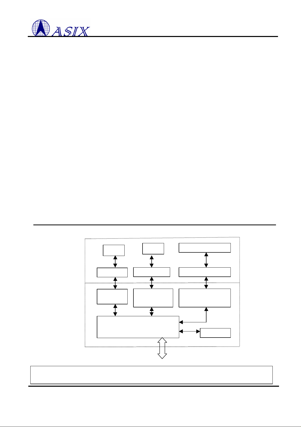
System Block Diagram
RJ11
MODEM
AX88190A
RJ45
10/100
PHY/TxRx
Home LAN PHY or
10M PHY/TxRx
PCMCIA I/F
This data sheet contains new products information. ASIX ELECTRONICS reserves the rights to modify product specification without notice. No liability
is assumed as a result of the use of this product. No rights under any patent accompany the sale of the product.
Always contact ASIX for possible updates before starting a design.
ASIX ELECTRONICS CORPORATION Frist Released Date : Dec/13/1999
2F, NO.13, Industry East Rd. II, Science-based Industrial Park, Hsin-Chu City, Taiwan, R.O.C.
TEL: 886-3-579-9500 FAX: 886-3-579-9558 http://www.asix.com.tw
Page 2

AX88190A PCMCIA Fast Ethernet MAC Controller
CONTENTS
1.0 INTRODUCTION...............................................................................................................................................5
1.1 GENERAL DESCRIPTION: ..................................................................................................................................... 5
1.2 AX88190A BLOCK DIAGRAM:............................................................................................................................5
1.3 AX88190A PIN CONNECTION DIAGRAM ............................................................................................................. 6
2.0 SIGNAL DESCRIPTION.................................................................................................................................... 7
2.1 PCMCIA BUS INTERFACE SIGNALS GROUP .........................................................................................................7
2.2 EEPROM SIGNALS GROUP.................................................................................................................................8
2.3 MII INTERFACE SIGNALS GROUP ..........................................................................................................................8
2.4 SNI INTERFACE PINS GROUP................................................................................................................................9
2.5 MODEM INTERFACE PINS GROUP .......................................................................................................................... 9
2.6 GENERAL PURPOSE I/O PINS GROUP.....................................................................................................................9
2.7 MISCELLANEOUS PINS GROUP ............................................................................................................................ 10
2.8 POWER ON CONFIGURATION SETUP SIGNALS CROSS REFERENCE TABLE.................................................................11
3.0 MEMORY AND I/O MAPPING ......................................................................................................................12
3.1 EEPROM MEMORY MAPPING ..........................................................................................................................12
3.2 ATTRIBUTE MEMORY MAPPING......................................................................................................................... 12
3.3 I/O MAPPING....................................................................................................................................................13
3.4 SRAM MEMORY MAPPING...............................................................................................................................13
4.0 REGISTERS OPERATION ..............................................................................................................................14
4.1 PCMCIA FUNCTION CONFIGURATION REGISTER SET OF LAN............................................................................14
4.1.1 Configuration Option Register of LAN (LCOR) Offset 3C0H (Read/Write)...............................................15
4.1.2 Configuration and Status Register of LAN (LCSR) Offset 3C2H (Read/Write)..........................................16
4.1.3 I/O Base Register 0/1 of LAN (LIOBASE0/1) Offset 3CAH/3CCH (Read/Write).......................................16
4.2 PCMCIA FUNCTION CONFIGURATION REGISTER SET OF MODEM.....................................................................17
4.2.1 Configuration Option Register of MODEM (MCOR) Offset 3E0H (Read/Write)....................................... 17
4.2.2 Configuration and Status Register of MODEM (MCSR) Offset 3E2H (Read/Write).................................. 18
4.2.3 I/O Base Register 0/1 of MODEM (MIOBASE0/1) Offset 3EAH/3ECH (Read/Write)...............................18
4.3 MAC CORE REGISTERS .................................................................................................................................... 19
4.3.1 Command Register (CR) Offset 00H (Read/Write) ....................................................................................21
4.3.2 Interrupt Status Register (ISR) Offset 07H (Read/Write)........................................................................... 21
4.3.3 Interrupt mask register (IMR) Offset 0FH (Write) ....................................................................................22
4.3.4 Data Configuration Register (DCR) Offset 0EH (Write)...........................................................................22
4.3.5 Transmit Configuration Register (TCR) Offset 0DH (Write).....................................................................22
4.3.6 Transmit Status Register (TSR) Offset 04H (Read) ...................................................................................23
4.3.7 Receive Configuration (RCR) Offset 0CH (Write) ....................................................................................23
4.3.8 Receive Status Register (RSR) Offset 0CH (Read)....................................................................................23
4.3.9 Inter-frame gap (IFG) Offset 16H (Read/Write)........................................................................................23
4.3.10 Inter-frame gap Segment 1(IFGS1) Offset 12H (Read/Write)..................................................................24
4.3.11 Inter-frame gap Segment 2(IFGS2) Offset 13H (Read/Write)..................................................................24
4.3.12 MII/EEPROM Management Register (MEMR) Offset 14H (Read/Write) ................................................. 24
4.3.13 Test Register (TR) Offset 15H (Write)..................................................................................................... 24
4.3.14 General Purpose Input Register (GPI) Offset 18H (Read) ......................................................................24
4.3.15 General Purpose I/O Register (GPIO) Offset 1AH (Read/Write).............................................................25
5.0 PCMCIA DEVICE ACCESS FUNCTIONS....................................................................................................26
5.1 ATTRIBUTE MEMORY ACCESS FUNCTION FUNCTIONS..........................................................................................26
5.2 I/O ACCESS FUNCTION FUNCTIONS..................................................................................................................... 26
2
ASIX ELECTRONICS CORPORATION
Page 3

AX88190A PCMCIA Fast Ethernet MAC Controller
6.0 ELECTRICAL SPECIFICATION AND TIMINGS .......................................................................................27
6.1 ABSOLUTE MAXIMUM RATINGS.........................................................................................................................27
6.2 GENERAL OPERATION CONDITIONS ................................................................................................................... 27
6.3 DC CHARACTERISTICS...................................................................................................................................... 27
6.4 A.C. TIMING CHARACTERISTICS........................................................................................................................28
6.4.1 XTAL / CLOCK......................................................................................................................................... 28
6.4.2 Reset Timing.............................................................................................................................................28
6.4.3 Attribute Memory Read Timing.................................................................................................................29
6.4.4 Attribute Memory Write Timing ................................................................................................................30
6.4.5 I/O Read Timing ....................................................................................................................................... 31
6.4.6 I/O Write Timing.......................................................................................................................................32
6.4.7 MII Timing................................................................................................................................................33
6.4.8 SNI Timing................................................................................................................................................34
7.0 PACKAGE INFORMATION........................................................................................................................... 35
APPENDIX A: APPLICATION NOTE................................................................................................................. 36
A.1 USING CRYSTAL 25MHZ OR 20MHZ.................................................................................................................36
A.2 USING OSCILLATOR 25MHZ OR 20MHZ............................................................................................................36
A.3 USING 60MHZ OSCILLATOR/CRYSTAL..............................................................................................................36
A.4 DUAL POWER (5V AND 3.3V) APPLICATION.......................................................................................................37
A.5 SINGLE POWER (3.3V) APPLICATION ................................................................................................................. 37
A.6 DUAL POWER (5V AND 3.3V) APPLICATION WITH 3.3V PHY .............................................................................38
APPENDIX B: AX88190 DESIGN CHANGES TO AX88190A ...........................................................................39
ERRATA OF AX88190A VERSION ED2..............................................................................................................40
DEMONSTRATION CIRCUIT : AX88190A + ETHERNET PHY + HOMEPNA 1M8 PHY ...........................41
REFERENCE BILL OF MATERIALS..................................................................................................................47
SPONSORS OF COMPONENTS ...........................................................................................................................48
SPONSORS OF COMPONENTS (CHINESE)......................................................................................................49
3
ASIX ELECTRONICS CORPORATION
Page 4

AX88190A PCMCIA Fast Ethernet MAC Controller
FIGURES
FIG - 1 AX88190A BLOCK DIAGRAM ...........................................................................................................................5
FIG - 2 AX88190A PIN CONNECTION DIAGRAM............................................................................................................6
TABLES
TAB - 1 PCMCIA BUS INTERFACE SIGNALS GROUP ........................................................................................................7
TAB - 2 EEPROM BUS INTERFACE SIGNALS GROUP........................................................................................................8
TAB - 3 MII INTERFACE SIGNALS GROUP........................................................................................................................8
TAB - 4 SERIAL NETWORK INTERFACE PINS GROUP ........................................................................................................9
TAB - 5 MODEM INTERFACE SIGNALS GROUP..................................................................................................................9
TAB - 6 GENERAL PURSOSE I/O PINS GROUP ................................................................................................................ 10
TAB - 7 MISCELLANEOUS PINS GROUP..........................................................................................................................10
TAB - 8 POWER ON CONFIGURATION SETUP TABLE...................................................................................................... 11
TAB - 9 EEPROM MEMORY MAPPING........................................................................................................................ 12
TAB - 10 ATTRIBUTE MEMORY MAPPING.................................................................................................................... 12
TAB - 11 I/O ADDRESS MAPPING................................................................................................................................ 13
TAB - 12 LOCAL MEMORY MAPPING........................................................................................................................... 13
TAB - 13 PCMCIA FUNCTION CONFIGURATION REGISTER MAPPING OF LAN............................................................... 14
TAB - 14 PCMCIA FUNCTION CONFIGURATION REGISTER MAPPING OF MODEM........................................................17
TAB - 15 PAGE 0 OF MAC CORE REGISTERS MAPPING.................................................................................................19
TAB - 16 PAGE 1 OF MAC CORE REGISTERS MAPPING.................................................................................................20
4
ASIX ELECTRONICS CORPORATION
Page 5
AX88190A PCMCIA Fast Ethernet MAC Controller
Registers
LOADER I/F
SD[15:0]
SA[9:0]
Ctl BUS
MII I/F
SMDIO
EEDO
SNI I/F
1.0 Introduction
1.1 General Description:
The AX88190A provides industrial standard NE2000 registers level compatable instruction set. Various drivers
are easy acquired, maintenance and usage with no pain and tears
The AX88190A Fast Ethernet Controller is a high performance and highly integrated PCMCIA bus Ethernet
Controller with embedded 8K*16 bit SRAM. The AX88190A contains a 16 bit PCMCIA interfaces to host CPU
and compliant with PC Card Standard – February 1995. The AX88190A implements both 10Mbps and
100Mbps Ethernet function based on IEEE802.3 / IEEE802.3u LAN standard. The AX88190A support
10Mbps/100Mbps media-independent interface (MII) and legacy pure 10Mbps SNI interface to simplify the
design. Using Serial Network Interface (SNI) transceiver, Home LAN PHY or 10BASE-2 BNC type media can be
supported. The AX88190A is built in interface to connect FAX/MODEM chipset with parallel bus interface.
The main difference between AX88190A and AX88190 are : 1) Replace memory I/F with SNI I/F. 2) Fix OE#
signal synchronous problem 3) Fix interrupt status can’t always clean up problem of AX88190. 4) Add 8 general
Purpose I/O ports. 5) Change MPD_SET (pin 74 -> pin 68) and PPD_SET (pin 76 -> pin 70) power on setup
pins location.
AX88190A use 128-pin LQFP low profile package, typical 25MHz operation, dual 5V and 3.3V CMOS process
with 5V I/O tolerance or pure 3.3V operation.
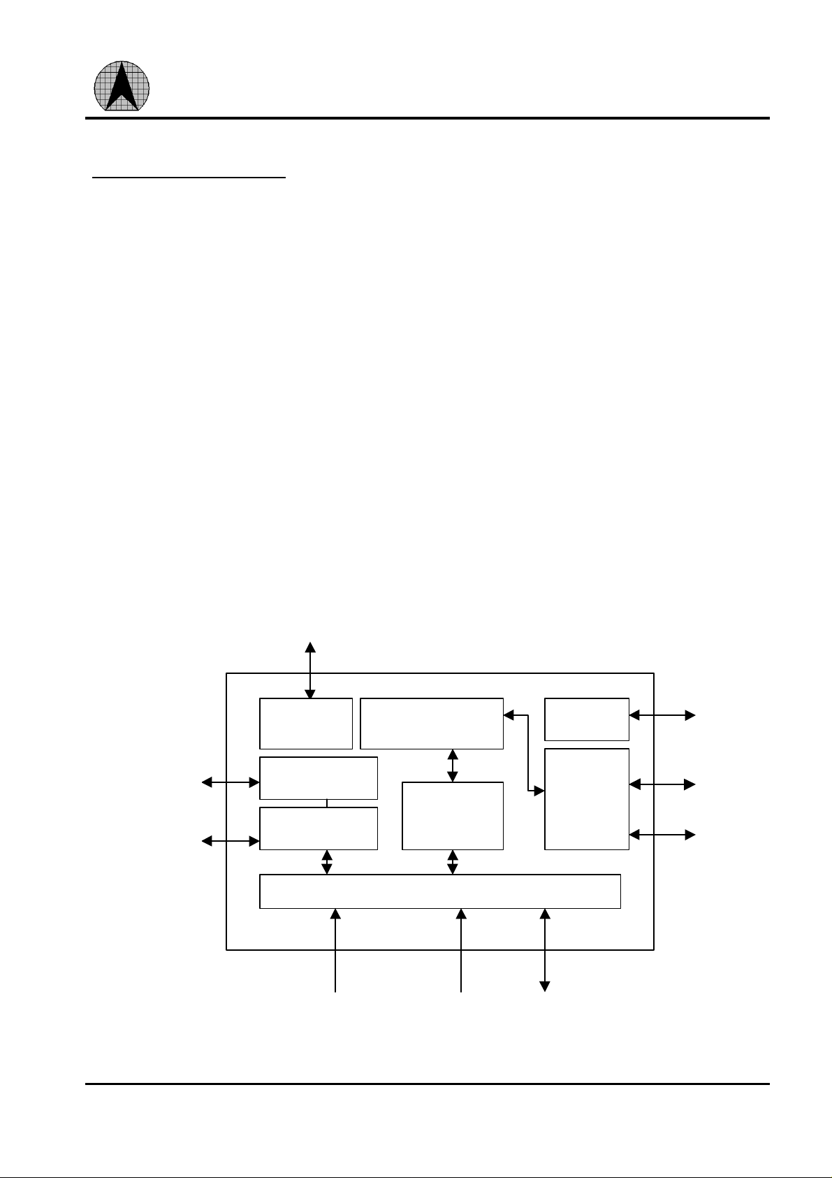
1.2 AX88190A Block Diagram:
SMDC
EECS
EECK
EEDI
GPI/O
MODEM
I/F
SEEPROM
NE2000/GPIO
8K* 16 SRAM
and Memory Arbiter
Remote
DMA
FIFOs
PCMCIA Interface
STA
MAC
Core
Fig - 1 AX88190A Block Diagram
5
ASIX ELECTRONICS CORPORATION
Page 6
AX88190A PCMCIA Fast Ethernet MAC Controller
SA[1]
HVDD
HVDD
SA[0]
SA[3]
SA[2]
SA[5]
SA[4]
SA[6]
SA[7]
SA[9]
SA[8]
IREQ#
IORD#
IOWR#
SD[15]
SD[14]
SD[13]
SD[12]
SD[11]
SD[10]
SD[9]
SD[8]
SD[6]
SD[5]
SD[7]
CE2#
CE1#
GPIO1#
GPIO0#
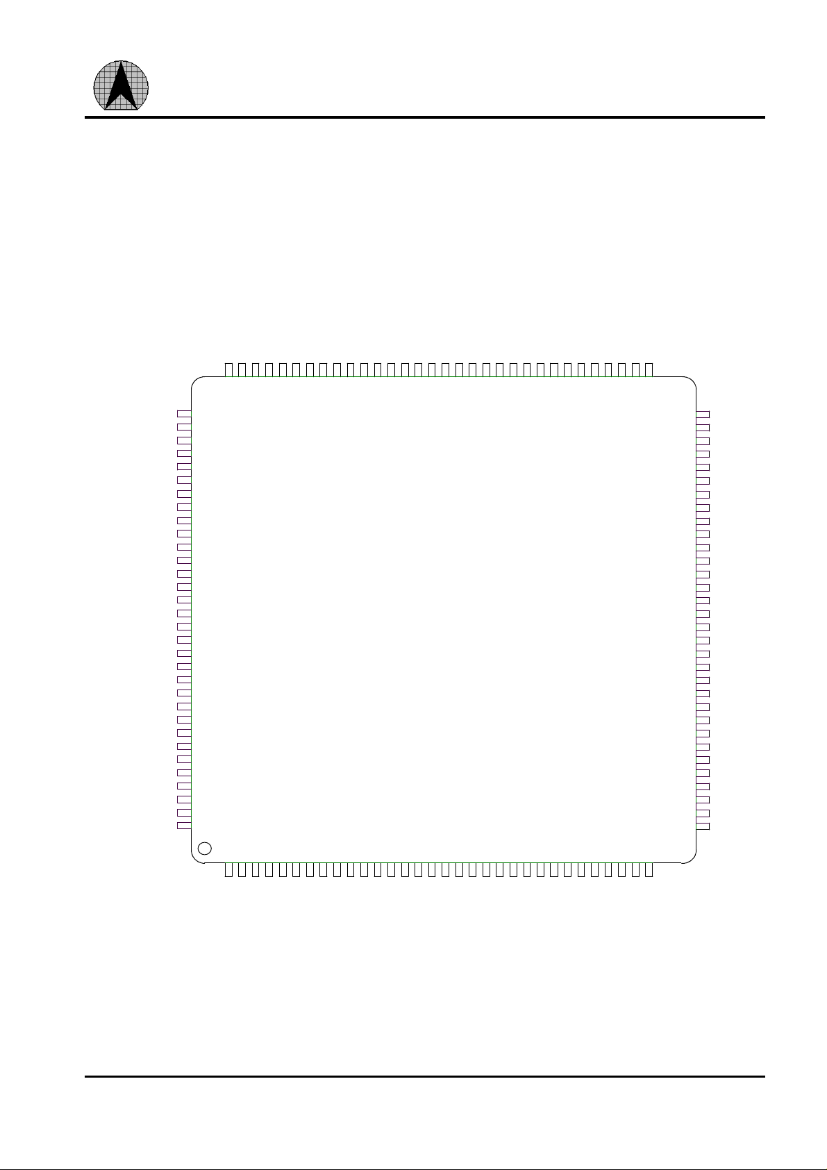
1.3 AX88190A Pin Connection Diagram
The AX88190A is housed in the 128-pin plastic light quad flat pack. See Fig - 2 AX88190A Pin
Connection Diagram.
TXD[1]
TXD[2]
TXD[3]
LVDD
CLKO
VSS
LCLK/XTALIN
XTALOUT
VSS
EECS
EECK
EEDI
EEDO
LVDD
MDCS#
MINT
MAUDIO
PPWDN
MRIN#
MPWDN
MRESET#
MRDY
VSS
IOIS16#
STSCHG#
SPKR#
REG#
INPACK#
WAIT#
LVDD
RESET
LVDD
97
98
99
100
101
102
103
104
105
106
107
108
109
110
111
112
113
114
115
116
117
118
119
120
121
122
123
124
125
126
127
128
TX_EN
TXD[0]
TX_CLK
94
95
96
3
1
2
MDC
VSS
93
928589
MDIO
RXD[3]
RXD[2]
90
RXD[1]
88
RXD[0]
RX_CLK
CRS
86
87
COL
RX_DV
84
83
RX_ER
VSS
SCRS
829181
SRXD
SRXC
78
797480
TEST
SCOL
77
76
SLINK#
NC
HVDD
EEPROM_SIZE
75
72
73
NC
71
AX88190A
PCMCIA
10/100BASE MAC
CONTROLLER
8
7
4
6
5
9
10
11
12
13
14
15
16
17
18
19
20
21
22
23
24
25
26
VSS
STXE
70
69
28
27
NC
STXC
CLK_DIV3#
STXD
66
65
68
67
32
31
29
30
64
63
62
61
60
59
58
57
56
55
54
53
52
51
50
49
48
47
46
45
44
43
42
41
40
39
38
37
36
35
34
33
HVDD
NC
NC
GPI0
GPI1
VSS
GPI2
GPI3
NC
NC
LVDD
NC
NC
NC
NC
VSS
NC
NC
NC
LVDD
GPIO2
GPIO3
VSS
VSS
SD[0]
SD[1]
SD[2]
SD[3]
VSS
SD[4]
Fig - 2 AX88190A Pin Connection Diagram
VSS
WE#
OE#
6
VSS
ASIX ELECTRONICS CORPORATION
Page 7

AX88190A PCMCIA Fast Ethernet MAC Controller
2.0 Signal Description
The following terms describe the AX88190A pin-out:
All pin names with the “#” suffix are asserted low.
The following abbreviations are used in following Tables.
I Input PU Pull Up
O Output PD Pull Down
I/O Input/Output P Power Pin
OD Open Drain
2.1 PCMCIA Bus Interface Signals Group
SIGNAL TYPE PIN NO. DESCRIPTION
SA[9:0] I 10 – 1 System Address : Signals SA[9:0] are address bus input lines which
enable direct address of up to 64K memory and I/O spaces on card.
SD[15:0] I/O 20 – 23,
25 – 38,
30 – 33,
35 – 38
IREQ# O 12 Interrupt Request : IREQ# is asserted to indicate the host system that
WAIT# O 125 Wait : This signal is set low to insert wait states during Remote DMA
REG# I 123 Attribute Memory and I/O Space Select : When the REG# signal is
IORD# I 15 I/O Read : The host asserts IORD# to read data from AX88190A I/O
IOWR# I 14 I/O Write : The host asserts IOWR# to write data into AX88190A I/O
OE# I 16 Output Enable : The OE# line is used to gate Memory Read data from
WE# I 13 Write Enable : The WE# signal is used for strobing Memory Write
IOIS16# O 120 I/O is 16 Bit Port : The IOIS16# is asserted when the address at the
INPACK# O 124 Input Port Acknowledge : The signal is asserted when the AX88190A
CE1#-CE2# I 18, 17 Card Enable : The CE1# enables even numbered address bytes and
BVD1_STSCHG# O 121 Battery Voltage Detect 1 / Status Change
BVD2_SPKR# O 122 Battery Voltage Detect 2 / Audio speaker out
System Data Bus : Signals SD[15:0] constitute the bi-directional data
bus.
the PC Card device requires host software service.
transfer.
asserted, access is limited to Attribute Memory and to the I/O space.
space.
space.
memory on PC Card
data into the memory on PC Card.
socket corresponds to an I/O address to which the card responds, and
the I/O port addressed is capable of 16-bit access.
is selected and can respond to and I/O read cycle at the address on the
address bus.
CE2# enables odd numbered address bytes
Tab - 1 PCMCIA bus interface signals group
7
ASIX ELECTRONICS CORPORATION
Page 8

AX88190A PCMCIA Fast Ethernet MAC Controller
2.2 EEPROM Signals Group
SIGNAL TYPE PIN NO. DESCRIPTION
EECS O 106 EEPROM Chip Select : EEPROM chip select signal.
EECK O 107 EEPROM Clock : Signal connected to EEPROM clock pin.
EEDI O 108 EEPROM Data In : Signal connected to EEPROM data input pin.
EEDO I/PU 109 EEPROM Data Out : Signal connected to EEPROM data output pin.
Tab - 2 EEPROM bus interface signals group
2.3 MII interface signals group
SIGNAL TYPE PIN NO. DESCRIPTION
RXD[3:0] I 90 – 87 Receive Data : RXD[3:0] is driven by the PHY synchronously with
respect to RX_CLK.
CRS I 85 Carrier Sense : Asynchronous signal CRS is asserted by the PHY
when either the transmit or receive medium is non-idle.
RX_DV I 83 Receive Data Valid : RX_DV is driven by the PHY synchronously
with respect to RX_CLK. Asserted high when valid data is present on
RXD [3:0].
RX_ER I 82 Receive Error : RX_ER ,is driven by PHY and synchronous to
RX_CLK, is asserted for one or more RX_CLK periods to indicate to
the port that an error has detected.
RX_CLK I 86 Receive Clock : RX_CLK is a continuous clock that provides the
timing reference for the transfer of the RX_DV,RXD[3:0] and
RX_ER signals from the PHY to the MII port of the repeater.
COL I 84 Collision : this signal is driven by PHY when collision is detected.
TX_EN O 95 Transmit Enable : TX_EN is transition synchronously with respect to
the rising edge of TX_CLK. TX_EN indicates that the port is
presenting nibbles on TXD [3:0] for transmission.
TXD[3:0] O 99 – 96 Transmit Data : TXD[3:0] is transition synchronously with respect to
the rising edge of TX_CLK. For each TX_CLK period in which
TX_EN is asserted, TXD[3:0] are accepted for transmission by the
PHY.
TX_CLK I 94 Transmit Clock : TX_CLK is a continuous clock from PHY. It
provides the timing reference for the transfer of the TX_EN and
TXD[3:0] signals from the MII port to the PHY.
MDC O 92 Station Management Data Clock : The timing reference for MDIO.
All data transfers on MDIO are synchronized to the rising edge of this
clock. MDC is a 2.5MHz frequency clock output.
MDIO I/O/PU 91 Station Management Data Input / Output : Serial data input/output
transfers from/to the PHYs . The transfer protocol conforms to the
IEEE 802.3u MII specification.
Tab - 3 MII interface signals group
8
ASIX ELECTRONICS CORPORATION
Page 9

AX88190A PCMCIA Fast Ethernet MAC Controller
2.4 SNI Interface pins group
SIGNAL TYPE PIN NO. DESCRIPTION
STXC I 66 Transmit Clock : this signal is driven by PHY with 20MHz clock.
STXD O 68 Transmit Data : STXD is transition synchronously with respect to the
rising edge of STXC. For each STXC period in which STXE is
asserted, STXD is accepted for transmission by the PHY.
STXE O 70 Transmit Enable : STXE is transition synchronously with respect to
the rising edge of STXC. STXE indicates that the port is presenting
data on STXD for transmission.
SCOL I 76 Collision : this signal is driven by PHY when collision is detected.
SRXC I 78 Receive Clock : SRXC is driven by PHY for received data
synchronization.
SRXD I 79 Receive Data : SRXD is driven by the PHY synchronously with respect
to SRXC.
SCRS I 80 Carrier Sense : Asynchronous signal SCRS is asserted by the PHY
when either the transmit or receive medium is non-idle.
SLINK# I/PU 74 Link indicator : Active low indicate the SNI interface is link to
network. When SNI is not used must keep the pin no connection or
pull high the signal.
Tab - 4 Serial Network Interface pins group
2.5 Modem interface pins group
Signal Name Type Pin No. Description
MRDY I/PU 118 Modem Ready : MRDY low indicates that modem is initializing the
modem after reset signal asserted or the modem is at SLEEP/STOP
mode.
MRESET# O 117 Modem Reset :This signal asserts low to reset the modem chipset.
MDCS# O 111 Modem Chip Select : This signal connected to modem chip select pin.
MPWDN O 116 Modem Power Down : Rockwell modem chipset, this signal asserts
low to let modem chipset into power down mode. AT&T modem
chipset, this signal asserts high to let modem chipset into power down
mode.
MINT I/PD 112 Modem Interrupt : This signal driven by modem chipset to active
interrupt.
MRIN# I/PU 115 Ring Input :This signal is driven by DAA’s ring detect circuit. When
a telephone ringing signal is being received.
MAUDIO I/PD 113 Modem Audio : This signal is passed to PCMCIA interface via SPKR.
Tab - 5 Modem interface signals group
2.6 General Purpose I/O pins group
Signal Name Type Pin No. Description
GPI[3] I 57 Read register offset 18h bit 3 value reflects this input value.
GPI[2] I 58 Read register offset 18h bit 2 value reflects this input value.
GPI[1] I 60 Read register offset 18h bit 1 value reflects this input value.
GPI[0] I 61 Read register offset 18h bit 0 value reflects this input value.
9
ASIX ELECTRONICS CORPORATION
Page 10

AX88190A PCMCIA Fast Ethernet MAC Controller
GPIO3# I/O 41 Default “1”. The pin reflects register offset 1Ah bit 3 inverted value.
GPIO2 I/O 42 Default “0”. The pin reflects register offset 1Ah bit 2 value.
GPIO1# I/O 43 Default “1”. The pin reflects register offset 1Ah bit 1 inverted value.
GPIO0# I/O 45 Default “1”. The pin reflects register offset 1Ah bit 0 inverted value.
Tab - 6 General Pursose I/O pins group
2.7 Miscellaneous pins group
SIGNAL TYPE PIN NO. DESCRIPTION
LCLK/XTALIN I 103 CMOS Local Clock : Typical a 25Mhz clock, +/- 100 ppm, 40%-60%
duty cycle. ( See application note also )
Crystal Oscillator Input : Typical a 25Mhz crystal, +/- 25 ppm can be
connected across XTALIN and XTALOUT.
XTALOUT O 104 Crystal Oscillator Output : Typical a 25Mhz crystal, +/- 25 ppm can be
connected across XTALIN and XTALOUT. If a single-ended external
clock (LCLK) is connected to XTALIN, the crystal output pin should
be left floating.
CLKO O 101 Clock Output : This clock is source from LCLK/XTALIN.
CLK_DIV3# I/PU 67 Clock Devide 3 Enable : Active low to enable the devided 3 circuit.
That internally devides LCLK/XTALIN input frequeny by 3 and then
feed into internal circuit for system clock used.
Default value set to logic high, this function is disabled.
PPWDN O 114 Phy Power Down : This pin connects to PHY chip power down mode
control input.
RESET I/PD 127 Reset
Reset is active high then place AX88190A into reset mode
immediately. During Falling edge the AX88190A loads the EEPROM
data.
TEST# I/PU 77
EEPROM SIZE I/PU 73 EEPROM SIZE = 0 : 93C46 128 byte type EEPROM is used.
NC N/A 46–48, 50–
53, 55-56,
LVDD P 44, 54,
100, 110,
126, 128
HVDD P 19, 29, 64,75Power Supply : +5V DC.
VSS P 11, 24, 34,
39, 40, 49,
59, 69, 81,
93, 102, 105,
119
Test Pin : Active LOW
The pin is just for test mode setting purpose only. Must be pull high
when normal operation.
EEPROM SIZE = 1 : 93C56 256 byte type EEPROM is used.
No Connection : for manufacturing test only.
Power Supply : +3.3V DC.
Note : for pure 3.3V single power solution, all the HVDD pin can
connect to +3.3V. Care should be taken that HVDD input power must
be greater or equal ( > = ) than LVDD.
Power Supply : +0V DC or Ground Power.
Tab - 7 Miscellaneous pins group
10
ASIX ELECTRONICS CORPORATION
Page 11

AX88190A PCMCIA Fast Ethernet MAC Controller
2.8 Power on configuration setup signals cross reference table
Signal Name Share with Description
MPD_SET STXD MPD_SET = 0 : MPWDN pin active high.
MPD_SET = 1 : MPWDN pin active low.
PPD_SET STXE PPD_SET = 0 : PPWDN pin active high.
PPD_SET = 1 : PPWDN pin active low.
All of the above signals are pull-up for default values.
Tab - 8 Power on Configuration Setup Table
11
ASIX ELECTRONICS CORPORATION
Page 12

AX88190A PCMCIA Fast Ethernet MAC Controller
3.0 Memory and I/O Mapping
There are four memory or I/O mapping used in AX88190A.
1. EEPROM Memory Mapping
2. Attribute Memory Mapping
3. I/O Mapping
4. Local Memory Mapping
3.1 EEPROM Memory Mapping
EEPROM OFFSET HIGH BYTE LOW BYTE
00H RESERVED WORD COUNT
01H CFH CFL
02H NODE-ID1 NODE ID 0
03H NODE ID 3 NODE ID 2
04H NODE ID 5 NODE ID 4
05H CHECKSUM RESERVED
06H – 10H RESERVED RESERVED
10H – FFH CIS CIS
Tab - 9 EEPROM Memory Mapping
Note : bit 3 register of LCOR in AX88190 is replaced by bit 0 of CFL in AX88190A
Bit 0 of CFL : Enable Power Down mode
this bit is set to 1, the LAN will go into power down mode. At power down mode AX88190A will disable MAC
transmitting and receiving operation. But the host interface will not be affected.
3.2 Attribute Memory Mapping
ATTRIBUTE MEMORY
OFFSET
0000H
03BFH
03C0H LCOR
03C2H LCCSR
03C4H 03C6H -
03CAH LIOBASE0
03CCH LIOBASE1
03CEH
03DFH
03E0H MCOR
03E2H MCCSR
03E4H 03E6H -
03EAH MIOBASE0
03ECH MIOBASE1
03EEH
03FFH
CONTENTS
CIS
RESERVED
RESERVED
Tab - 10 Attribute Memory Mapping
12
ASIX ELECTRONICS CORPORATION
Page 13

AX88190A PCMCIA Fast Ethernet MAC Controller
3.3 I/O Mapping
SYSTEM I/O OFFSET FUNCTION
0000H
001FH
Tab - 11 I/O Address Mapping
3.4 SRAM Memory Mapping
OFFSET FUNCTION
0000H
03BFH
03C0H LCOR *1
03C2H LCCSR *1
03C4H 03C6H -
03CAH LIOBASE0 *1
03CCH LIOBASE1 *1
03CEH
03DFH
03E0H MCOR *1
03E2H MCCSR *1
03E4H 03E6H -
03EAH MIOBASE0 *1
03ECH MIOBASE1 *1
03EEH
03FFH
0400H NODE ID 0
0401H NODE ID 1
0402H NODE ID 2
0403H NODE ID 3
0404H NODE ID 4
0405H NODE ID 5
0406H
07FFH
4000H
7FFFH
MAC CORE REGISTER
CIS *1
RESERVED
RESERVED
RESERVED
8K X 16
SRAM BUFFER
Tab - 12 Local Memory Mapping
13
ASIX ELECTRONICS CORPORATION
Page 14

AX88190A PCMCIA Fast Ethernet MAC Controller
4.0 Registers Operation
There are three register sets in AX88190A :
The PCMCIA function configuration registers of LAN.
The PCMCIA function configuration registers of MODEM.
The MAC core register.
4.1 PCMCIA Function Configuration Register Set of LAN
REGISTER NAME OFFSET
LCOR CONFIGURATION OPTION REGISTER 3C0H
LCSR CONFIGURATION AND STATUS REGISTER 3C2H
LIOBASE0 I/O BASED REGISTER 0 3CAH
LIOBASE1 I/O BASED REGISTER 1 3CCH
Tab - 13 PCMCIA Function Configuration Register Mapping of LAN
14
ASIX ELECTRONICS CORPORATION
Page 15

AX88190A PCMCIA Fast Ethernet MAC Controller
4.1.1 Configuration Option Register of LAN (LCOR) Offset 3C0H (Read/Write)
FIELD R/W/C DESCRIPTION
7 R/W Software Reset
Assert this bit will reset the LAN function of AX88190A. Return a 0 to this bit will leave
the LAN function of AX88190A in a post-reset state as same as that following a hardware
reset. The value of this bit is 0 at power-on.
6 R/W Level IRQ
This bit should be set to 1, the AX88190A always generates Level Mode Interrupt.
5:0 R/W Function Configuration Index
These six bits are used to indicate entry of the card configuration table locate in the CIS.
The default value is 0
.
On multifunction PC Card,
Bit 5, Bit 4, Bit 3 : MODEM I/O base registers
Bit 5 Bit 4 Bit 3 LAN I/O base MODEM I/O base
0 0 0 300H Decided by MIOBASE registers
0 0 1 320H 2f8H
0 1 0 340H 3e8H
0 1 1 360H 2e8H
1 0 0 380H Decided by MIOBASE registers
1 0 1 200H 2f8H
1 1 0 220H 3e8H
1 1 1 240H 2e8H
Bit 2 : Enable IREQ# Routing
If bit 0 of LCOR is set to 0, this bit is ignored.
If bit 0 of LCOR is set to 1 and this bit is set to 1, the LAN will generate interrupt request
via IREQ# signal. If this bit is set to 0, the LAN will not generate interrupt request via
IREQ# line.
Bit 1 : Enable Base and Limit Registers
If bit 0 of LCOR is set to 0, this bit is ignored.
If bit 0 of LCOR is set to 1 and this bit is set to 1,only I/O addresses that are qualified by
the Base and Limit registers are passed to LAN function. If this bit is set to 0,all I/O
addresses are passed to LAN function.
Bit 0 : Enable Function
If this bit is set to 0, the LAN function is disabled.
If this bit is set to 1, the LAN function is enabled.
15
ASIX ELECTRONICS CORPORATION
Page 16

AX88190A PCMCIA Fast Ethernet MAC Controller
4.1.2 Configuration and Status Register of LAN (LCSR) Offset 3C2H (Read/Write)
FIELD R/W/C DESCRIPTION
7:3 - Reserved
2 R/W PPwrDwn : PHY power down setting
While this bit set to 1, PPWDN pin (pin 114) will be active to force PHY chip into power
down mode. As for PPWDN is active high or active low. Please refer section 2.7 Power on
configuration setup signal cross reference table.
1 R Intr : Interrupt Request
The LAN function will set this bit to 1 when it need interrupt service and set it to 0 when it
is not request interrupt service.
0 R IntrAck : Interrupt Acknowledge
This bit will be 0. The Intr will reflect the status of interrupt requesting.
4.1.3 I/O Base Register 0/1 of LAN (LIOBASE0/1) Offset 3CAH/3CCH (Read/Write)
The I/O Base registers (LIOBASE0 and LIOBASE1) determine the base address of the I/O range used to
access the LAN specific registers (MAC Core Registers).
I/O Base Register 0
FIELD R/W/C DESCRIPTION
7:0 R/W Base I/O address bit 7 – 0.
I/O Base Register 1
FIELD R/W/C DESCRIPTION
7:0 R/W Base I/O address bit 15 – 8.
16
ASIX ELECTRONICS CORPORATION
Page 17

AX88190A PCMCIA Fast Ethernet MAC Controller
4.2 PCMCIA Function Configuration Register Set of MODEM
REGISTER NAME OFFSET
MCOR CONFIGURATION OPTION REGISTER 3E0H
MCSR CONFIGURATION AND STATUS REGISTER 3E2H
MIOBASE0 I/O BASED REGISTER 0 3EAH
MIOBASE1 I/O BASED REGISTER 1 3ECH
Tab - 14 PCMCIA Function Configuration Register Mapping of MODEM
4.2.1 Configuration Option Register of MODEM (MCOR) Offset 3E0H (Read/Write)
FIELD R/W/C DESCRIPTION
7 R/W Software Reset
Assert this bit will reset the MODEM function of AX88190A. Return a 0 to this bit will
leave the MODEM function of AX88190A in a post-reset state as same as that following
a hardware reset. The value of this bit is 0 at power-on.
6 R/W Level IRQ
This bit should be set to 1, the AX88190A always generates Level Mode Interrupt.
5:0 R/W Function Configuration Index
These six bits are used to indicate entry of the card configuration table locate in the CIS.
The default value is 0
.
On multifunction PC Card,
Bit 5, Bit4 : Reserved
Bit 3 : MINT route to STSCHG#
If bit 0 of MCOR is set to 0, this bit is ignored.
If both bit 0 and bit 2 of MCOR are set to 1 and this bit is set to 1, the MODEM will route
interrupt request to STSCHG# signal. If this bit is set to 0, the MODEM will generate
interrupt request via IREQ# line.
Bit 2 : MINT route to IREQ# (Enable IREQ# Routing)
If bit 0 of MCOR is set to 0, this bit is ignored.
If bit 0 of MCOR is set to 1 and this bit is set to 1, the MODEM will generate interrupt
request via IREQ# signal. If this bit is set to 0, the MODEM will not generate interrupt
request via IREQ# line.
Bit 1 : Enable Base and Limit Registers
If bit 0 of MCOR is set to 0, this bit is ignored.
If bit 0 of MCOR is set to 1 and this bit is set to 1,only I/O addresses that are qualified
by the Base and Limit registers are passed to MODEM function. If this bit is set to 0,all
I/O addresses are passed to LAN function.
Bit 0 : Enable Function
If this bit is set to 0, the MODEM function is disabled.
If this bit is set to 1, the MODEM function is enabled.
17
ASIX ELECTRONICS CORPORATION
Page 18

AX88190A PCMCIA Fast Ethernet MAC Controller
4.2.2 Configuration and Status Register of MODEM (MCSR) Offset 3E2H (Read/Write)
FIELD R/W/C DESCRIPTION
7:3 - Reserved
2 R/W MPwrDwn : Modem power down setting
While this bit set to 1, MPWDN pin (pin 116) will be active to force modem chip into power
down mode. As for MPWDN is active high or active low. Please refer section 2.7 Power on
configuration setup signal cross reference table.
1 R Intr : Interrupt Request
The LAN function will set this bit to 1 when it need interrupt service and set it to 0 when it
is not request interrupt service.
0 R IntrAck : Interrupt Acknowledge
This bit will be 0. The Intr will reflect the status of interrupt requesting.
4.2.3 I/O Base Register 0/1 of MODEM (MIOBASE0/1) Offset 3EAH/3ECH (Read/Write)
The I/O Base registers (MIOBASE0 and MIOBASE1) determine the base address of the I/O range used to
access the MODEM specific registers.
I/O Base Register 0
FIELD R/W/C DESCRIPTION
7:0 R/W Base I/O address bit 7 – 0.
I/O Base Register 1
FIELD R/W/C DESCRIPTION
7:0 R/W Base I/O address bit 15 – 8.
18
ASIX ELECTRONICS CORPORATION
Page 19

AX88190A PCMCIA Fast Ethernet MAC Controller
4.3 MAC Core Registers
All registers of MAC Core are 8-bit wide and mapped into pages which are selected by PS in the Command
Register.
PAGE 0 (PS1=0,PS0=0)
OFFSET READ WRITE
00H Command Register
( CR )
01H Page Start Register
( PSTART )
02H Page Stop Register
( PSTOP )
03H Boundary Pointer
( BNRY )
04H Transmit Status Register
( TSR )
05H Number of Collisions Register
( NCR )
06H Current Page Register
( CPR )
07H Interrupt Status Register
( ISR )
08H Current Remote DMA Address 0
( CRDA0 )
09H Current Remote DMA Address 1
( CRDA1 )
0AH Reserved Remote Byte Count 0
0BH Reserved Remote Byte Count 1
0CH Receive Status Register
( RSR )
0DH Frame Alignment Errors
( CNTR0 )
0EH CRC Errors
( CNTR1 )
0FH Missed Packet Errors
( CNTR2 )
10H
11H
12H IFGS1 IFGS1
13H IFGS2 IFGS2
14H MII/EEPROM Access MII/EEPROM Access
15H - Test Register
16H Inter-frame Gap (IFG) Inter-frame Gap (IFG)
17H – 18H Reserved Reserved
19H GPI Reserved
1AH GPIO GPIO
1BH - 1EH Reserved Reserved
1FH Reset Reserved
Data Port Data Port
Command Register
( CR )
Page Start Register
( PSTART )
Page Stop Register
( PSTOP )
Boundary Pointer
( BNRY )
Transmit Page Start Address
( TPSR )
Transmit Byte Count Register 0
( TBCR0 )
Transmit Byte Count Register 1
( TBCR1 )
Interrupt Status Register
( ISR )
Remote Start Address Register 0
( RSAR0 )
Remote Start Address Register 1
( RSAR1 )
( RBCR0 )
( RBCR1 0
Receive Configuration Register
( RCR )
Transmit Configuration Register ( TCR )
Data Configuration Register
( DCR )
Interrupt Mask Register
( IMR )
Tab - 15 Page 0 of MAC Core Registers Mapping
19
ASIX ELECTRONICS CORPORATION
Page 20

AX88190A PCMCIA Fast Ethernet MAC Controller
PAGE 1 (PS1=0,PS0=1)
OFFSET READ WRITE
00H Command Register
( CR )
01H Physical Address Register 0
( PARA0 )
02H Physical Address Register 1
( PARA1 )
03H Physical Address Register 2
( PARA2 )
04H Physical Address Register 3
( PARA3 )
05H Physical Address Register 4
( PARA4 )
06H Physical Address Register 5
( PARA5 )
07H Current Page Register
( CPR )
08H Multicast Address Register 0
( MAR0 )
09H Multicast Address Register 1
( MAR1 )
0AH Multicast Address Register 2
( MAR2 )
0BH Multicast Address Register 3
( MAR3 )
0CH Multicast Address Register 4
( MAR4 )
0DH Multicast Address Register 5
( MAR5 )
0EH Multicast Address Register 6
( MAR6 )
0FH Multicast Address Register 7
( MAR7 )
10H
11H
12H Inter-frame Gap Segment 1
13H Inter-frame Gap Segment 2
14H MII/EEPROM Access MII/EEPROM Access
15H - Test Register
16H Inter-frame Gap (IFG) Inter-frame Gap (IFG)
17H – 18H Reserved Reserved
19H GPI Reserved
1AH GPIO GPIO
1BH - 1EH Reserved Reserved
1FH Reset Reserved
Data Port Data Port
IFGS1
IFGS2
Command Register
( CR )
Physical Address Register 0
( PAR0 )
Physical Address Register 1
( PAR1 )
Physical Address Register 2
( PAR2 )
Physical Address Register 3
( PAR3 )
Physical Address Register 4
( PAR4 )
Physical Address Register 5
( PAR5 )
Current Page Register
( CPR )
Multicast Address Register 0
( MAR0 )
Multicast Address Register 1
( MAR1 )
Multicast Address Register 2
( MAR2 )
Multicast Address Register 3
( MAR3 )
Multicast Address Register 4
( MAR4 )
Multicast Address Register 5
( MAR5 )
Multicast Address Register 6
( MAR6 )
Multicast Address Register 7
( MAR7 )
Inter-frame Gap Segment 1
IFGS1
Inter-frame Gap Segment 2
IFGS2
Tab - 16 Page 1 of MAC Core Registers Mapping
20
ASIX ELECTRONICS CORPORATION
Page 21

AX88190A PCMCIA Fast Ethernet MAC Controller
4.3.1 Command Register (CR) Offset 00H (Read/Write)
FIELD NAME DESCRIPTION
7:6 PS1,PS0 PS1,PS0 : Page Select
The two bit selects which register page is to be accessed.
PS1 PS0
0 0 page 0
0 1 page 1
5:3 RD2,RD1
,RD0
2 TXP TXP : Transmit Packet
1 START START :
0 STOP STOP : Stop AX88190A
RD2,RD1,RD0 : Remote DMA Command
These three encoded bits control operation of the Remote DMA channel. RD2 could be set
to abort any Remote DMA command in process. RD2 is reset by AX88190A when a Remote
DMA has been completed. The Remote Byte Count should be cleared when a Remote DMA
has been aborted. The Remote Start Address are not restored to the starting address if the
Remote DMA is aborted.
RD2 RD1 RD0
0 0 0 Not allowed
0 0 1 Remote Read
0 1 0 Remote Write
0 1 1 Not allowed
1 X X Abort / Complete Remote DMA
This bit could be set to initiate transmission of a packet
This bit is used to active AX88190A operation.
This bit is used to stop the AX88190A operation.
4.3.2 Interrupt Status Register (ISR) Offset 07H (Read/Write)
FIELD NAME DESCRIPTION
7 RST Reset Status :
Set when AX88190A enters reset state and cleared when a start command is issued to the
CR. Writing to this bit is no effect.
6 RDC Remote DMA Complete
Set when remote DMA operation has been completed
5 CNT Counter Overflow
Set when MSB of one or more of the Tally Counters has been set.
4 OVW Over Write : Set when receive buffer ring storage resources have been exhausted.
3 TXE Transmit Error
Set when packet transmitted with one or more of the following errors
Excessive collisions
FIFO Under-run
2 RXE Receive Error
Indicates that a packet was received with one or more of the following errors
CRC error
Frame Alignment Error
FIFO Overrun
Missed Packet
1 PTX Packet Transmitted
Indicates packet transmitted with no error
0 PRX Packet Received
Indicates packet received with no error.
21
ASIX ELECTRONICS CORPORATION
Page 22

AX88190A PCMCIA Fast Ethernet MAC Controller
4.3.3 Interrupt mask register (IMR) Offset 0FH (Write)
FIELD NAME DESCRIPTION
7 - Reserved
6 RDCE DMA Complete Interrupt Enable. Default “low” disabled.
5 CNTE Counter Overflow Interrupt Enable. Default “low” disabled.
4 OVWE Overwrite Interrupt Enable. Default “low” disabled.
3 TXEE Transmit Error Interrupt Enable. Default “low” disabled.
2 RXEE Receive Error Interrupt Enable. Default “low” disabled.
1 PTXE Packet Transmitted Interrupt Enable. Default “low” disabled.
0 PRXE Packet Received Interrupt Enable. Default “low” disabled.
4.3.4 Data Configuration Register (DCR) Offset 0EH (Write)
FIELD NAME DESCRIPTION
7 RDCR Remote DMA always completed
6:2 - Reserved
1 BOS Byte Order Select
0: MS byte placed on AD15:AD8 and LS byte on AD7-AD0 (80X86).
1: MS byte placed on AD7::AD0 and LS byte on AD15:AD0(68K)
0 WTS Word Transfer Select
0 : Selects byte-wide DMA transfers.
1 : Selects word-wide DMA transfers.
4.3.5 Transmit Configuration Register (TCR) Offset 0DH (Write)
FIELD NAME DESCRIPTION
7 FDU Full Duplex :
This bit indicates the current media mode is Full Duplex or not.
0 : Half duplex
1 : Full duplex
6 PD Pad Disable
0 : Pad will be added when packet length less than 60.
1 : Pad will not be added when packet length less than 60.
5 RLO Retry of late collision
0 : Don’t retransmit packet when late collision happens.
1 : Retransmit packet when late collision happens.
4:3 - Reserved
2:1 LB1,LB0 Encoded Loop-back Control
These encoded configuration bits set the type of loop-back that is to be performed.
LB1 LB0
Mode 0 0 0 Normal operation
Mode 1 0 1 Internal NIC loop-back
Mode 2 1 0 PHYcevisor loop-back
0 CRC Inhibit CRC
0 : CRC appended by transmitter.
1 : CRC inhibited by transmitter.
22
ASIX ELECTRONICS CORPORATION
Page 23

AX88190A PCMCIA Fast Ethernet MAC Controller
4.3.6 Transmit Status Register (TSR) Offset 04H (Read)
FIELD NAME DESCRIPTION
7 OWC Out of window collision
6:4 - Reserved
3 ABT Transmit Aborted
Indicates the AX88190A aborted transmission because of excessive collision.
2 COL Transmit Collided
Indicates that the transmission collided at least once with another station on the network.
1 - Reserved
0 PTX Packet Transmitted
Indicates transmission without error.
4.3.7 Receive Configuration (RCR) Offset 0CH (Write)
FIELD NAME DESCRIPTION
7 INT_RG Interrupt Regeneration
0 : Enable interrupt regeneration function in multifunction application. (default) But must
set CIS relative Enable function first, than the function will be open.
1: Disable
6
5 MON Monitor Mode
4 PRO PRO : Promiscuous Mode
3 AM AM : Accept Multicast
2 AB AB : Accept Broadcast
1 AR AR : Accept Runt
0 SEP SEP : Save Error Packet
Reserved
-
0 : Normal Operation
1 : Monitor Mode, the input packet will be checked on NODE ADDRESS and CRC but not
buffered into memory.
Enable the receiver to accept all packets with a physical address.
Enable the receiver to accept packets with a multicast address. That multicast address must
pass the hashing array.
Enable the receiver to accept broadcast packet.
Enable the receiver to accept runt packet.
Enable the receiver to accept and save packets with error.
4.3.8 Receive Status Register (RSR) Offset 0CH (Read)
FIELD NAME DESCRIPTION
7 - Reserved
6 DIS Receiver Disabled
5 PHY Multicast Address Received.
4 MPA Missed Packet
3 FO FIFO Overrun
2 FAE Frame alignment error.
1 CR CRC error.
0 PRX Packet Received Intact
4.3.9 Inter-frame gap (IFG) Offset 16H (Read/Write)
FIELD NAME DESCRIPTION
7 - Reserved
6:0 IFG Inter-frame Gap. Default value 15H.
23
ASIX ELECTRONICS CORPORATION
Page 24

AX88190A PCMCIA Fast Ethernet MAC Controller
4.3.10 Inter-frame gap Segment 1(IFGS1) Offset 12H (Read/Write)
FIELD NAME DESCRIPTION
7 - Reserved
6:0 IFG Inter-frame Gap Segment 1. Default value 1cH.
4.3.11 Inter-frame gap Segment 2(IFGS2) Offset 13H (Read/Write)
FIELD NAME DESCRIPTION
7 - Reserved
6:0 IFG Inter-frame Gap Segment 2. Default value 11H.
4.3.12 MII/EEPROM Management Register (MEMR) Offset 14H (Read/Write)
FIELD NAME DESCRIPTION
7 EECLK EECLK
EEPROM Clock
6 EEO EEO
EEPROM Data Out
5 EEI EEI
EEPROM Data In
4 EECS EECS
EEPROM Chip Select
3 MDO MDO
MII Data Out
2 MDI MDI
MII Data In
1 MDIR MII STA MDIO signal Direction
MII Read Control Bit, assert this bit let MDIO signal as the input signal. Deassert this bit
let MDIO as output signal.
0 MDC MDC
MII Clock
4.3.13 Test Register (TR) Offset 15H (Write)
FIELD NAME DESCRIPTION
7 - Reserved
6 MPSEL Media Priority Select : default value is logic 0
MPSEL /SLINK Media Selected
0 0 SNI
0 1 MII
1 x Depand on MPSET bit
5 MPSET Media Set by Program : The signal is valid only when MPSEL is set to high.
When MPSET is logic 0 , SNI is selected.
When MPSET is logic 1 , MII is selected.
4 TF16T Test for Collision, default value is logic 0
3 TPE Test pin Enable, default value is logic 0
2:0 IFG Select Test Pins Output, default value is logic 0
4.3.14 General Purpose Input Register (GPI) Offset 18H (Read)
FIELD NAME DESCRIPTION
7:4 - Reserved
3 GPI3 This register reflects GPI[3] input value
2 GPI2 This register reflects GPI[2] input value
1 GPI1 This register reflects GPI[1] input value
0 GPI0 This register reflects GPI[0] input value
24
ASIX ELECTRONICS CORPORATION
Page 25

AX88190A PCMCIA Fast Ethernet MAC Controller
4.3.15 General Purpose I/O Register (GPIO) Offset 1AH (Read/Write)
FIELD NAME DESCRIPTION
7:6 - Reserved
5 CTL Default “1”. And must keep it to logic 1 always.
4 - Reserved
3 GPIO3 Default “0”. The register reflects to GPIO3# pin with inverted value.
2 GPIO2 Default “0”. The register reflects to GPIO2 pin directly.
1 GPIO1 Default “0”. The register reflects to GPIO1# pin with inverted value.
0 GPIO0 Default “0”. The register reflects to GPIO0# pin with inverted value.
25
ASIX ELECTRONICS CORPORATION
Page 26

AX88190A PCMCIA Fast Ethernet MAC Controller
5.0 PCMCIA Device Access Functions
5.1 Attribute Memory access function functions.
Attribute Memory Read function
Function Mode REG# CE2# CE1# SA0 OE# WE# SD[15:8] SD[7:0]
Standby Mode X H H X X X High-Z High-Z
Byte Access (8 bits) L
L
Word Access (16 bits) L L L X L H Not Valid Even-Byte
Odd Byte Only Access L L H X L H Not Valid High-Z
Attribute Memory Write function
Function Mode REG# CE2# CE1# SA0 OE# WE# SD[15:8] SD[7:0]
Standby Mode X H H X X X X X
Byte Access (8 bits) L
L
Word Access (16 bits) L L L X H L X Even-Byte
Odd Byte Only Access L L H X H L X X
H
H
H
H
L
L
L
L
L
H
L
H
L
L
H
H
H
H
L
L
High-Z
High-Z
X
X
Even-Byte
Not Valid
Even-Byte
X
5.2 I/O access function functions.
I/O Read function
Function Mode REG# CE2# CE1# SA0 OE# WE# SD[15:8] SD[7:0]
Standby Mode X H H X X X High-Z High-Z
Byte Access (8 bits) L
L
Word Access (16 bits) L L L L L H Odd-Byte Even-Byte
I/O Inhibit H X X X L H High-Z High-Z
Odd Byte Only Access L L H X L H Odd-Byte High-Z
I/O Write function
Function Mode REG# CE2# CE1# SA0 IORD# IOWR# SD[15:8] SD[7:0]
Standby Mode X H H X X X X X
Byte Access (8 bits) L
L
Word Access (16 bits) L L L L H L Odd-Byte Even-Byte
I/O Inhibit H X X X H L X X
Odd Byte Only Access L L H X H L Odd-Byte X
H
H
H
H
L
L
L
L
L
H
L
H
L
L
H
H
H
H
L
L
High-Z
High-Z
X
X
Even-Byte
Odd-Byte
Even-Byte
Odd-Byte
26
ASIX ELECTRONICS CORPORATION
Page 27

AX88190A PCMCIA Fast Ethernet MAC Controller
6.0 Electrical Specification and Timings
6.1 Absolute Maximum Ratings
Description SYM Min Max Units
Operating Temperature Ta 0 +85
Storage Temperature Ts -55 +150
Supply Voltage HVdd -0.3 +6 V
Supply Voltage LVdd -0.3 +4.6 V
Input Voltage HVin
LVin
Output Voltage HVout
LVin
Lead Temperature (soldering 10 seconds maximum) Tl -55 +220
Note : Stress above those listed under Absolute Maximum Ratings may cause permanent damage to the device. Exposure
to Absolute Maximum Ratings conditions for extended period, adversely affect device life and reliability.
Note : The power supply voltages must always fulfill HVdd >= LVdd inequality.
-0.3
-0.3
-0.3
-0.3
HVdd+0.5
LVdd+0.5
HVdd+0.5
LVdd+0.5
°C
°C
V
V
V
V
°C
6.2 General Operation Conditions
Description SYM Min Tpy Max Units
Operating Temperature Ta 0 25 +75
Supply Voltage HVdd
LVdd
Note : The power supply voltages must always fulfill HVdd >= LVdd inequality.
+4.75V
+2.70
+3.00
+5.00V
+3.00
+3.30
+5.25V
+3.30
+3.60
°C
V
V
V
6.3 DC Characteristics
(Vdd=5.0V, Vss=0V, Ta=0°C to 75°C)
Description SYM Min Tpy Max Units
Low Input Voltage Vil - 0.8 V
High Input Voltage Vih 2 - V
Low Output Voltage Vol - 0.4 V
High Output Voltage Voh Vdd-0.4 - V
Input Leakage Current Iil -1 +1 uA
Output Leakage Current Iol -1 +1 uA
(Vdd=3.0V to 3.6V, Vss=0V, Ta=0°C to 75°C)
Description SYM Min Tpy Max Units
Low Input Voltage Vil - 0.8 V
High Input Voltage Vih 1.9 - V
Low Output Voltage Vol - 0.4 V
High Output Voltage Voh Vdd-0.4 - V
Input Leakage Current Iil -1 +1 uA
Output Leakage Current Iol -1 +1 uA
Description SYM Min Tpy Max Units
Power Consumption (Dual power) DPt5v
DPt3v
Power Consumption (Single power 3.3V) SPt3v 48 mA
27
17
31
ASIX ELECTRONICS CORPORATION
mA
mA
Page 28

AX88190A PCMCIA Fast Ethernet MAC Controller
6.4 A.C. Timing Characteristics
6.4.1 XTAL / CLOCK
Thigh
LCLK/XTALIN
Tr Tf Tlow
Tcyc
CLKO Tod
Symbol Description Min Typ. Max Units
Tcyc CYCLE TIME
Thigh CLK HIGH TIME
Tlow CLK LOW TIME
Tr/Tf CLK SLEW RATE
Tod LCLK/XTALIN TO CLKO OUT DELAY
16 20 24 ns
16 20 24 ns
1 - 4 ns
* Note : The Tcyc can be from 16.6ns to 50ns, that is frequency from 60MHz to 20MHz.
40* ns
10
6.4.2 Reset Timing
LCLK
RESET
Symbol Description Min Typ. Max Units
Trst Reset pulse width
100 - - LClk
28
ASIX ELECTRONICS CORPORATION
Page 29

AX88190A PCMCIA Fast Ethernet MAC Controller
6.4.3 Attribute Memory Read Timing
TcR
Ta(A) Th(A)
A[9:0], REG#
Ta(CE) Tv(A)
CE#
Tsu(A) Ta(OE) Th(CE)
OE#
Tv(WT-OE) Tw(WT) Tdis(CE)
WAIT#
D[15:0] DATA Valid
Tsu(CE)
Ten(OE) Tv(WT) Tdis(OE)
Symbol Description Min Typ. Max Units
TcR READ CYCLE TIME
Ta(A) ADDRESS ACCESS TIME
Ta(CE) CARD ENABLE ACCESS TIME
Ta(OE) OUTPUT ENABLE ACCESS TIME
Tdis(OE) OUTPUT DISABLE TIME FROM OE#
Ten(OE) OUTPUT ENABLE TIME FROM OE#
Tv(A) DATA VALID FROM ADDRESS CHANGE
Tsu(A) ADDRESS SETUP TIME
Th(A) ADDRESS HOLD TIME
Tsu(CE) CARD ENABLE SETUP TIME
Th(CE) CARD ENABLE HOLD TIME
Tv(WT-OE) WAIT# VALID FROM OE#
Tw(WT) WAIT# PULSE WIDTH
Tv(WT) DATA SETUP FOR WAIT# RELEASED
300 - - ns
- - 120 ns
- - 100 ns
- - 100 ns
0.5 - - ns
- - 100 ns
0 - - ns
30 - - ns
20 - - ns
0 - - ns
20 - - ns
- - 10 ns
- - 200 ns
100 - - ns
29
ASIX ELECTRONICS CORPORATION
Page 30

AX88190A PCMCIA Fast Ethernet MAC Controller
6.4.4 Attribute Memory Write Timing
TcW
A[9:0], REG#
Tsu(CE-WEH)
CE# Tsu(CE)
Tsu(A-WEH) Th(CE)
OE#
Tsu(A) Tw(WE) Trec(WE)
WE#
Tv(WT-WE) Tv(WT)
Tw(WT) Th(OE-WE)
WAIT#
Tsu(OE-WE) Tsu(D-WEH) Th(D)
D[15:0](Din) DATA Input Establish
Tdis(WE) Ten(OE)
D[15:0](Dout)
Tdis(OE) Ten(WE)
Symbol Description Min Typ. Max Units
TcW WRITE CYCLE TIME
Tw(WE) WRITE PULSE WIDTH
Tsu(A) ADDRESS SETUP TIME
Tsu(A-WEH) ADDRESS SETUP TIME FOR WE#
Tsu(CE-WEH) CARD ENABLE SETUP TIME FOR WE#
Tsu(D-WEH) DATA SETUP TIME FOR WE#
Th(D) DATA HOLD TIME
Trec(WE) WRITE RECOVER TIME
Tdis(WE) OUTPUT DISABLE TIME FROM WE#
Tdis(OE) OUTPUT DISABLE TIME FROM OE#
Ten(WE) OUTPUT ENABLE TIME FROM WE#
Ten(OE) OUTPUT ENABLE TIME FROM OE#
Tsu(OE-WE) OUTPUT ENABLE SETUP TIME FROM OE#
Th(OE-WE) OUTPUT ENABLE HOLD TIME FROM OE#
Tsu(CE) CARD ENABLE SETUP TIME
Th(CE) CARD ENABLE HOLD TIME
Tv(WT-WE) WAIT# VALID FROM WE#
Tw(WT) WAIT# PULSE WIDTH
Tv(WT) WE# HIGH FROM WAIT# RELEASED
250 - - ns
150 - - ns
30 - - ns
180 - - ns
180 - - ns
80 - - ns
30 - - ns
30 - - ns
- - 5 ns
- - 5 ns
5 - - ns
5 - - ns
10 - - ns
10 - - ns
0 - - ns
20 - - ns
- - 15 ns
- - 200 ns
0 - - ns
30
ASIX ELECTRONICS CORPORATION
Page 31

AX88190A PCMCIA Fast Ethernet MAC Controller
6.4.5 I/O Read Timing
A[9:0]
REG#
TsuREG ThREG
TsuCE ThCE
CE#
Tw
IORD#
TsuA TdrINPACK
INPACK#
TdfINPACK TdrIOIS16
IOIS16#
TdfIOIS16 Td
Tdr(WT)
WAIT#
TdfWT Tw(WT) Th
D[15:0] DATA Valid
ThA
Symbol Description Min Typ. Max Units
Td DATA DELAY AFTER IORD#
Th DATA HOLD FOLLOWING IORD#
Tw IORD# WIDTH TIME
TsuA ADDRESS SETUP BEFORE IORD#
ThA ADDRESS HOLD BEFORE IORD#
TsuCE CE# SETUP BEFORE IORD#
ThCE CE# HOLD BEFORE IORD#
TsuREG REG# SETUP BEFORE IORD#
ThREG REG# HOLD BEFORE IORD#
TdfINPACK INPACK# DELAY FALLING FROM IORD#
TdrINPACK INPACK# DELAY RISING FROM IORD#
TdfIOIS16 IOIS16# DELAY FALLING FROM ADDRESS*
TdrIOIS16 IOIS16# DELAY RISING FROM ADDRESS*
TdfWT WAIT# DELAY FALLING FROM IORD#
Tdr(WT) DATA DELAY FROM WAIT# RISING
Tw(WT) WAIT# WIDTH TIME
- - 50 ns
0.5 - - ns
165 - - ns
70 - - ns
20 - - ns
5 - - ns
20 - - ns
5 - - ns
0 - - ns
0 - 10 ns
- - 10 ns
- - 10 ns
- - 0 ns
- - 5 ns
- - 0 us
- - 100 ns
* Note : The address includes REG# and CE1# signal
31
ASIX ELECTRONICS CORPORATION
Page 32

AX88190A PCMCIA Fast Ethernet MAC Controller
6.4.6 I/O Write Timing
A[9:0]
REG#
TsuREG ThREG
TsuCE ThCE
CE#
Tw
IOWR#
TsuA TdrIOIS16
IOIS16#
TdfIOIS16
TdrIOWR
WAIT#
TdfWT Tw(WT) Th
D[15:0] DATA
ThA
Tsu
Symbol Description Min Typ. Max Units
Tsu DATA SETUP BEFORE IOWR#
Th DATA HOLD FOLLOWING IOWR#
Tw IOWR# WIDTH TIME
TsuA ADDRESS SETUP BEFORE IOWR#
ThA ADDRESS HOLD BEFORE IOWR#
TsuCE CE# SETUP BEFORE IOWR#
ThCE CE# HOLD BEFORE IOWR#
TsuREG REG# SETUP BEFORE IOWR#
ThREG REG# HOLD BEFORE IOWR#
TdfIOIS16 IOIS16# DELAY FALLING FROM ADDRESS*
TdrIOIS16 IOIS16# DELAY RISING FROM ADDRESS*
TdfWT WAIT# DELAY FALLING FROM IOWR#
Tw(WT) WAIT# WIDTH TIME
TdrIOWR IOWR# HIGH FROM WAIT# HIGH
60 - - ns
30 - - ns
165 - - ns
70 - - ns
20 - - ns
5 - - ns
20 - - ns
5 - - ns
0 - - ns
- - 10 ns
- - 0 ns
- - ** ns
- - ** ns
0 - - us
*Note : The address includes REG# and CE1# signal
** Note : There is no wait state while I/O Write operation
32
ASIX ELECTRONICS CORPORATION
Page 33

AX88190A PCMCIA Fast Ethernet MAC Controller
6.4.7 MII Timing
Ttclk Ttch Ttcl
TXCLK
Ttv Tth
TXD<3:0>
TXEN
Trclk Trch Trcl
RXCLK
Trs Trh
RXD<3:0>
RXDV
Trs1
RXER
Symbol Description Min Typ. Max Units
Ttclk Cycle time(100Mbps)
Ttclk Cycle time(10Mbps)
Ttch high time(100Mbps)
Ttch high time(10Mbps)
Trch low time(100Mbps)
Trch low time(10Mbps)
Ttv Clock to data valid
Tth Data output hold time
Trclk Cycle time(100Mbps)
Trclk Cycle time(10Mbps)
Trch high time(100Mbps)
Trch high time(10Mbps)
Trcl low time(100Mbps)
Trcl low time(10Mbps)
Trs data setup time
Trh data hold time
Trs1 RXER data setup time
- 40 - ns
- 400 - ns
14 - 26 ns
140 - 260 ns
14 - 26 ns
140 - 260 ns
- - 20 ns
5 - - ns
- 40 - ns
- 400 - ns
14 - 26 ns
140 - 260 ns
14 - 26 ns
140 - 260 ns
6 - - ns
10 - - ns
10 - - ns
33
ASIX ELECTRONICS CORPORATION
Page 34

AX88190A PCMCIA Fast Ethernet MAC Controller
6.4.8 SNI Timing
Ttclk Ttch Ttcl
STXC
Ttv Tth
STXD
STXE
Trclk Trch Trcl
SRXC
Trs Trh
SRXD
SCRS
Symbol Description Min Typ. Max Units
Ttclk Cycle time(10Mbps)
Ttch high time(10Mbps)
Trch low time(10Mbps)
Ttv Clock to data valid
Tth Data output hold time
Trclk Cycle time(10Mbps)
Trch high time(10Mbps)
Trcl low time(10Mbps)
Trs data setup time
Trh data hold time
- 100 - ns
45 - 55 ns
45 - 55 ns
- - 26 ns
5 - - ns
- 100 - ns
45 - 55 ns
45 - 55 ns
10 - - ns
5 - - ns
34
ASIX ELECTRONICS CORPORATION
Page 35

AX88190A PCMCIA Fast Ethernet MAC Controller
7.0 Package Information
Hd
He
E
D
pin 1
b
e
A
A2 A1
L1
L
θ
MILIMETERSYMBOL
MIN. NOM MAX
A1 0.1
A2 1.3 1.4 1.5
A 1.7
b 0.155 0.16 0.26
D 13.90 14.00 14.10
E 13.90 14.00 14.10
e 0.40
Hd 15.60 16.00 16.40
He 15.60 16.00 16.40
L 0.30 0.50 0.70
L1 1.00
θ
0 10
35
ASIX ELECTRONICS CORPORATION
Page 36

AX88190A PCMCIA Fast Ethernet MAC Controller
Appendix A: Application Note
A.1 Using Crystal 25MHz or 20MHz
AX88190A To PHY
CLKO 25MHz
XTALIN XTALOUT
25MHz
Crystal
8pf 2Mohm 8pf
Note : The capacitors (8pf) may be various depend on the specification of crystal. While designing, please
refer to the suggest circuit provided by crystal supplier.
A.2 Using Oscillator 25MHz or 20MHz
AX88190A To PHY
CLKO 20MHz
XTALIN XTALOUT
NC
3.3V Power OSC 20MHz
A.3 Using 60MHz Oscillator/Crystal
AX88190A To PHY
CLK_DIV3#
Pull Low 20MHz
Devided
By 3
XTALIN XTALOUT
CLKO 60MHz
NC
3.3V Power OSC 60MHz
36
ASIX ELECTRONICS CORPORATION
Page 37

AX88190A PCMCIA Fast Ethernet MAC Controller
DAA
MAGNETIC
EEPROM
DAA
MAGNETIC
EEPROM
A.4 Dual power (5V and 3.3V) application
RJ45RJ11
+5V +5V
+5V HVdd +5V
+3.3V LVdd
AX88190A
A.5 Single power (3.3V) application
PHY/TxRxMODEM
+5V PCMCIA I/F
RJ45RJ11
+3.3V
(option for core logic)
+3.3V +3.3V
+3.3V HVdd +3.3V
+3.3V LVdd
AX88190A
PHY/TxRxMODEM
+3.3V PCMCIA I/F
37
ASIX ELECTRONICS CORPORATION
Page 38

AX88190A PCMCIA Fast Ethernet MAC Controller
AX88190A
PHY
A.6 Dual power (5V and 3.3V) application with 3.3V PHY
The 510 and 1K Ohm resisters are just for voltage adjustment
RXD[3:0]
CRS
RX_DV
RX_ER
RX_CLK
COL
TX_EN
TXD[3:0]
TX_CLK
MDC
MDIO
RXD[3:0]
CRS
RX_DV
RX_ER
RX_CLK
COL
TX_EN
TXD[3:0]
TX_CLK
MDC
MDIO
510 ohm 1k ohm
38
ASIX ELECTRONICS CORPORATION
Page 39

AX88190A PCMCIA Fast Ethernet MAC Controller
Appendix B: AX88190 design changes to AX88190A
Please refer to following circuit diagram that implement in AX88190 PWB and follow the following
four steps.
1. Remove AX88190 and replace with AX88190A
2. Remove 2 pieces of buffer memory(32k*8 SRAM). Because they are not necessary anymore.
3. Remove 74F86 and 74F74 TTL IC
4. Shorten the jumper shown as below circuit diagram lable “Jumper for future use”
From AX88190
Pin 101
CLK25M
OE_# OE_M#
From PCMCIA
Connector
Pin 9
U2A
1
2
74F86
3
Jumper for future use
12
11
2
3
D
CLK
D
CLK
10
PR
13
4
PR
CL
1
U1B
74F74
9
Q
8
Q
CL
U1A
74F74
5
Q
Q
6
To AX88190
Pin 16
39
ASIX ELECTRONICS CORPORATION
Page 40

AX88190A PCMCIA Fast Ethernet MAC Controller
Errata of AX88190A Version ED2
1. SNI (Serial Network Interface) has bug for HomePNA application.
Solution: Using MII interface for HomePNA solution. Refer to “Demonstration Circuit”
on page 39 to 44.
40
ASIX ELECTRONICS CORPORATION
Page 41

AX88190A 10/100Mbps PCMCIA Fast Ethernet MAC Controller
Demonstration Circuit : AX88190A + Ethernet PHY + HomePNA 1M8 PHY
IREQ#
IOIS16#
WAIT#
INPACK#
SPKR#
STSCHG#
GND
SD3
SD4
SD5
SD6
SD7
CE1#
OE#
SA9
SA8
WE#
IREQ#
VCC
SA7
SA6
SA5
SA4
SA3
SA2
SA1
SA0
SD0
SD1
SD2
IOIS16#
GND
IREQ#
IOIS16#
WAIT#
INPACK#
SPKR#
STSCHG#
U4
1
GND
2
D3
3
D4
4
D5
5
D6
6
D7
7
CE1#
8
A10
9
OE#
10
A11
11
A9
12
A8
13
A13
14
A14
15
WE#
16
IREQ#
17
VCC
18
VPP1
19
A16
20
A15
21
A12
22
A7
23
A6
24
A5
25
A4
26
A3
27
A2
28
A1
29
A0
30
D0
31
D1
32
D2
33
IOIS16#
34
GND
PCMCIA-68
ICM-68FYC-OM03
GND
CD1#
D11
D12
D13
D14
D15
CE2#
VS1#
IORD#
IOWR#
A17
A18
A19
A20
A21
VCC
VPP2
A22
A23
A24
A25
VS2#
RESET
WAIT#
INPACK#
REG#
SPKR#
STSCHG#
D10
CD2#
GND
CE1#
OE#
WE#
CE2#
IORD#
IOWR#
RESET
REG#
3.3V
GND
VCC
35
GND
36
GND
37
SD11
SD12
38
39
SD13
SD14
40
SD15
41
CE2#
42
43
IORD#
44
IOWR#
45
46
47
48
49
50
VCC
51
52
53
54
55
56
57
58
RESET
59
WAIT#
INPACK#
60
REG#
61
SPKR#
62
63
STSCHG#
SD8
64
D8
65
D9
SD9
66
SD10
GND
67
GND
68
CE1#
OE#
WE#
CE2#
IORD#
IOWR#
RESET
REG#
3.3V
GND
VCC
SA[0..9]
SD[0..15]
R40 : option for 3.3V card tpye.
R40
1k
VCC
GND
AX88190AL 10BASE-T/100BASE-TX & 1M HomePNA
Application with DP83846A & DP83851 PHYceiver.
(reference only)
VCC
GND
+
C8
4.7uF/16V
C32
0.01u
4.7uF/16V
U7
AMS117
+
C1
C12
0.01u
TAB/OUT
OUTIN
ADJ/GND
4
23
1
+
C10
4.7uF/16V
3.3V
C9
0.01u
41
ASIX ELECTRONICS CORPORATION
Page 42

AX88190A 10/100Mbps PCMCIA Fast Ethernet MAC Controller
SA[0..9]
SD[0..15]
CE1#
OE#
WE#
CE2#
IORD#
IOWR#
RESET
REG#
RXER
RXDV
RXCLK
COL
CRS
RXD[0..3]
TXCLK
MDIO
3.3V
GND
VCC
CE1#
OE#
WE#
CE2#
IORD#
IOWR#
RESET
REG#
RXER
RXDV
RXCLK
COL
CRS
RXD[0..3]
TXCLK
MDIO
RXD0
RXD1
RXD2
RXD3
3.3V
GND
5V
5V
3.3V
SD0
SD1
SD2
SD3
SD4
SD5
SD6
SD7
SD8
SD9
SD10
SD11
SD12
SD13
SD14
SD15
SA0
SA1
SA2
SA3
SA4
SA5
SA6
SA7
SA8
SA9
CE1#
OE#
WE#
IREQ#
IOIS16#
CE2#
IORD#
IOWR#
RESET
WAIT#
INPACK#
REG#
SPKR#
STSCHG#
120
127
125
124
123
122
121
100
110
126
128
102
105
119
1
2
3
4
5
6
7
8
9
10
38
37
36
35
33
32
31
30
28
27
26
25
23
22
21
20
18
16
13
12
17
15
14
19
29
64
75
44
54
11
24
34
39
40
49
59
69
81
93
U5
SA0
SA1
SA2
SA3
SA4
SA5
SA6
SA7
SA8
SA9
SD0
SD1
SD2
SD3
SD4
SD5
SD6
SD7
SD8
SD9
SD10
SD11
SD12
SD13
SD14
SD15
CE1#
OE#
WE#
IREQ#
IOIS16#
CE2#
IORD#
IOWR#
RESET
WAIT#
INPACK#
REG#
SPKR#
STSCHG#
HVDD
HVDD
HVDD
HVDD
LVDD
LVDD
LVDD
LVDD
LVDD
LVDD
VSS
VSS
VSS
VSS
VSS
VSS
VSS
VSS
VSS
VSS
VSS
VSS
VSS
AX88190AL
MDCS#
MMINT
MAUDIO
MRIN#
MPWDN
MRESET#
MRDY
MPD_SET
PPD_SET
SLINK#
RX_ER
RX_DV
RX_CLK
RXD0
RXD1
RXD2
RXD3
TX_CLK
TX_EN
TXD0
TXD1
TXD2
TXD3
MDIO
EECS
EECK
EEDI
EEDO
PPWDN
CLKO25M
LCLK/XTALIN
XTALOUT
TEST#
EEPROM SIZE
COL
CRS
MDC
GPI1
GPI0
111
112
113
115
116
RESET#
117
118
68
70
74
82
RXER
RXDV
83
COL
84
CRS
85
RXCLK
86
RXD0
87
RXD1
88
RXD2
89
RXD3
90
TXCLK
94
TXEN
95
TXD0
96
TXD1
97
98
TXD2
TXD3
99
MDIO
91
MDC
92
EECS
106
EESK
107
EEDI
108
EEDO
109
114
101
XIN
103
XOUT
104
(R22 : option for test)
77
73
(R23 : option for use 93C46)
60
61
(R42 : option for RESERVED)
R6
10K
R25 10K
R21 10k
R22 10K
R23 10K
R41 10K
R42 10K
R2
4.7K
R8
20
3.3V
3.3V
3.3V
PCLK
5V
GND
3.3V
GND
EECS
EESK
EEDI
EEDO
IREQ#
IOIS16#
WAIT#
INPACK#
SPKR#
STSCHG#
RESET#
TXEN
MDC
PCLK
1
2
3
4 5
XIN
IREQ#
IOIS16#
WAIT#
INPACK#
SPKR#
STSCHG#
RESET#
TXEN
TXD[0..3]
MDC
PCLK
U1
C25
0.1u
C19
0.1u
VCC
NC
NC
8
7
6
C24
0.1u
XOUT
CS
SK
DI
DO GND
93C56
Y1 25MHZ-CRYSTAL
R7
2M
C18
8p
C23
0.1u
C20
0.1u
C17
8p
5V
GND
C16
0.1u
42
ASIX ELECTRONICS CORPORATION
Page 43

TXD[0..3]
TXEN
MDC
MDIO
RESET#
PCLK
3.3V
GND
AX88190A 10/100Mbps PCMCIA Fast Ethernet MAC Controller
RXD3
RXD2
TXD[0..3]
TXEN
MDC
MDIO
RESET#
PCLK
3.3V
GND
TXCLK
RXCLK
3.3V
R19 20
R18 20
R3 4.7K
TXD3
TXD2
TXD1
TXD0
TXEN
RXD3
RXD2
RXD1
RXD0
RXDV
COL
CRS
MDIO
MDC
PCLK
3.3V
3.3VA1
3.3VA2
U3
36
TXD3
35
TXD2
34
TXD1
33
TXD0/TXD
32
TX_EN
31
TX_CLK
23
RXD3/PHYAD0
24
RXD2/CMDDIS#
25
RXD1/HI_POWER_EN#
26
RXD0/RXD/LOW_SPEED_EN#
27
RX_DV/GPSI_SEL#
28
RX_CLK
37
COL/MDIO_INT_EN#
38
CRS/PIN_INTRP_EN#
21
MDIO
22
MDC
45
X1
46
X2
19
IO_VDD1
29
IO_VDD2
39
CORE_VDD
48
ANA_VDD1
5
ANA_VDD2
11
ANA_VDD3
20
IO_GND1
30
IO_GND2
40
CORE_GND
41
CORE_SUB(0V)
47
ANA_GND1
3
ANA_GND2
6
ANA_GND3
10
ANA_GND4
1
SUB_GND1
2
SUB_GND2
9
SUB_GND3
DP83851
TIP
RING
RBIAS
LED_COL/PHYAD2
LED_ACT/PHYAD1
LED_SPEED/PHYAD3
LED_POWER/PHYAD4
RESET#
RESERVED
RESERVED
RESERVED
RESERVED
RESERVED
RXD1
RXD0
7
TIP
8
RING
4
R20
9.31K
1%
17
COLLED
18
ACTLED
SPDLED
16
PWRLED
15
RESET#
44
12
13
14
42
43
3.3V
GND
3.3V
GND
RXD3
COLLED
C4
0.1u
TXCLK
COL
RXCLK
RXD[0..3]
RXDV
CRS
TIP
RING
HACTLED
HCOLLED
HSPDLED
ACTLED
COLLED
SPDLED
ACTLED
SPDLED
PWRLED
L2
F.B.
TXCLK
COL
RXCLK
RXD[0..3]
RXDV
CRS
TIP
RING
HACTLED
HCOLLED
HSPDLED
3.3VA1
R14
510
R16
510
R17
510
R1
4.7K
R4
4.7K
R13
4.7K
R5
4.7K
R15
4.7K
C7
+
4.7uF/16V
C5
0.1u
HACTLED
HCOLLED
HSPDLED
GND
Set PHY address to 00000.
3.3V
GND
C13
0.1u
C14
0.1u
C21
0.1u
L1
F.B.
C26
0.1u
3.3VA2
C15
0.1u
43
ASIX ELECTRONICS CORPORATION
Page 44

AX88190A 10/100Mbps PCMCIA Fast Ethernet MAC Controller
TXCLK
GND
RXCLK
R45
4.7K
TXEN
TXD[0..3]
MDIO
MDC
RESET#
PCLK
RDP
RDN
GND
R44 20
R12 4.7K
R27 20
3.3V
3.3VA1
3.3VA2
3.3V
TXEN
TXD[0..3]
MDIO
MDC
RESET#
PCLK
RDP
RDN
3.3V
GND
R45 : Setting FDPX LED
(OPTION)
TXD3
TXD2
TXD1
TXD0
TXEN
RXD3
RXD2
RXD1
RXD0
RXDV
RXER
COL
CRS
MDIO
MDC
PCLK
U8
59
TXD3
58
TXD2
55
TXD1
54
TXD0
52
TX_EN
51
TX_CLK
50
TX_ER
38
RXD3
39
RXD2
40
RXD1
41
RXD0
44
RX_DV
45
RX_CLK
46
RX_ER/PAUSE_EN#
60
COL
61
CRS/LED_CFG#
36
MDIO
37
MDC
67
X1
66
X2
35
IO_VDD
43
IO_VDD
57
IO_VDD
65
IO_VDD
24
CORE_VDD
49
CORE_VDD
72
CORE_VDD
4
ANA_VDD
7
ANA_VDD1
12
ANA_VDD2
14
ANA_VDD3
34
IO_GND
42
IO_GND
53
IO_GND
56
IO_GND
64
IO_GND
23
CORE_GND
48
CORE_GND
73
CORE_GND
2
ANA_GND
6
ANA_GND
9
ANA_GND
13
ANA_GND
15
ANA_GND
18
ANA_GND
19
SUB_GND
76
SUB_GND
79
SUB_GND
DP83846A
RESET#
RBIAS
LED_DPLX/PHY0
LED_COL/PHY1
LED_GDLNK/PHY2
LED_TX/PHY3
LED_RX/PHY4
LED_SPEED
AN_EN
AN_1
AN_0
RESERVED
RESERVED
RESERVED
RESERVED
RESERVED
RESERVED
RESERVED
RESERVED
RESERVED
RESERVED
RESERVED
RESERVED
RESERVED
RESERVED
RESERVED
RESERVED
RESERVED
TD+
TD-
RD+
RD-
RXD3
RXD2
RXD1
RXD0
TDP3.3V
16
TDN
17
11
RDP
RDN
10
62
RESET#
3
33
FLED
CLED
32
31
LLED
TLED
30
RLED
29
28
SLED
27
26
25
1
5
8
20
21
22
47
63
68
69
70
71
74
75
77
78
80
R47
9.31K
BY PASS CAP WITH DIGITAL POWER SUPPLY
3.3V
GND
BY PASS CAP WITH ANALOG POWER SUPPLY
3.3V
GND
RXER
RXDV
COL
RXCLK
RXD[0..3]
TXCLK
CRS
TDP
TDN
ACTLED
LNKLED
SPDLED
C41
0.01u
L4
F.B.
RXER
RXDV
COL
RXCLK
RXD[0..3]
TXCLK
CRS
TDP
TDN
ACTLED
LNKLED
SPDLED
C29
0.1u
3.3VA1
PHYAD0
PHYAD1
PHYAD2
PHYAD3
PHYAD4
TLED
RLED
C27
0.1u
C39
0.1u
D2 1N4148
D1 1N4148
Transmit Activity : used R29.
Receive Activity : used R30.
Transmit/Receive Activity :
D1 & D2 & R31.
C35
C34
0.1u
0.1u
3.3V
GND
Set PHY ADDRESS TO 00011
FLED
CLED
LLED
TLED
RLED
R43 4.7K
R26 4.7K
R24 4.7K
R28 4.7K
R11 4.7K
To PCMJ15 Connect
SLED
LLED
R33 510
R32 510
R29 510
R31 510
R30 510
C33
0.1u
L3
F.B.
C22
0.01u
SPDLED
LNKLED
ACTLED
3.3VA2
C31
0.1u
3.3V
GND
44
ASIX ELECTRONICS CORPORATION
Page 45

AX88190A 10/100Mbps PCMCIA Fast Ethernet MAC Controller
TDP
TDN
TIP
RING
HSPDLED
HCOLLED
HACTLED
SPDLED
LNKLED
ACTLED
3.3V
GND
TDN
TDP
RDN
RDP
TDP
TDN
TIP
RING R9
HSPDLED
HCOLLED
HACTLED
SPDLED
LNKLED
ACTLED
3.3V
GND
C36
10p
C30
10p
R36
49.9
1%
R35
49.9
1%
R34
49.9
1%
3.3V
R46
49.9
1%
C38
10p
TIP
RING
C40
0.1u
6
7
8
1
2
3
U6
CT
TD+
TD-
RD+
RDCT
16ST0009P
R10
49.9
1%
C2
P0800SA
CT
TX+
TX-
RX+
RX-
CT
49.9
1%
3.3V
11
10
9
16
15
14
TXTX+
RXRX+
C6
4
6
1
2
R37
75
0.1u
U2
TUT+
TUTZ+
Z-
LHR002
R48
75
R39
RDN
RDP
LTIP
11
TIP+
RING-
C+
C-
R38
75
75
LRING
9
14
13
C3
0.01u/2KV
RXRX+
HACTLED
HCOLLED
ACTLED
LNKLED
HSPDLED
SPDLED
LTIP
LRING
GND
TXTX+
C42
10p
RDN
RDP
J1
15
14
13
12
11
10
9
8
7
6
5
4
3
2
1
PCMCIA-15
RMC-E15MY-OM-MA2
C28
0.01u
C37
0.01u
C43 0.01u
R49 1M
C11
0.01u/2KV
45
CHASSIS
ASIX ELECTRONICS CORPORATION
Page 46

AX88190A 10/100Mbps PCMCIA Fast Ethernet MAC Controller
J5
1
2
3
4
5
6
7
8
CON8
J3
1
2
3
4
5
6
7
8
CON8
HACTLED
HCOLLED
HSPDLED
GND
R45
R78
LTIP
LRING
ACTLED
LNKLED
SPDLED
GND
RXRX+
TXTX+
LTIP
LRING
TX+
TX-
RX+
RX-
R45
R78
J2
1
NC
2
A1
3
TIP
4
RING
5
A2
6
NC
RJ11-S
J4
1
2
3
6
4
5
7
8
RJ45N
HCOLLED
HACTLED
HSPDLED
ACTLED
LNKLED
SPDLED
D6
HomePNA collision LED
LED
D8
HomePNA activity LED
LED
D5
HomePNA speed LED
LED
D7
10/100M collision LED
LED
D4
10/100M link LED
LED
D3
10/100Mspeed LED
LED
46
ASIX ELECTRONICS CORPORATION
Page 47

AX88190A 10/100Mbps PCMCIA Fast Ethernet MAC Controller
Reference Bill Of Materials
Item Quantity Reference Part Reamrk
1 2 C18,C17 8p 0603
2 4 C30,C36,C38,C42 10p 0603
3 8 C9,C12,C22,C28,C32,C37,C41,C43 0.01uF 0603
4 22 C4,C5,C6,C13,C14,C15,C16,C19,C20,C21,C23,C24,C25,C26,C27,C29,C31,C33,C34,C35,C39,C40 0.1uF 0603
5 4 C1,C7,C8,C10 4.7uF/16V 1206
6 2 C11,C3 0.01u/2KV 1206
7 1 C2 P0800SA *1
8 2 D2,D1 1N4148 SMD
9 6 D3,D4,D5,D6,D7,D8 LED DIP
10 4 L1,L2,L3,L4 F.B 1206
11 5 R8,R18,R19,R27,R44 20 0603
12 4 R37,R38,R39,R48 75 0603
13 5 R9,R10,R35,R46,R34,R36 49.9 1% 0603
14 5 R14,R16,R17,R32,R33 510 0603
14-1 1 R31 330 0603
15 13 R1,R2,R3,R4,R5,R11,R12,R13,R15,R24,R26,R28,R43 4.7K 0603
16 2 R47,R20 9.31K 1% 0603
17 4 R6,R21,R25,R42 10K 0603
18 1 R49 1M 0603
19 1 R7 2M 0603
20 1 U5 AX88190AL TQFP
21 1 U1 93C56 SMD
22 1 U2 LHR002 *2
23 1 U6 16ST0009P *2
24 1 U3 DP83851 *3
25 1 U8 DP83846A *3
26 1 U7 AMS117 SMD
27 1 Y1 25MHZ CRYSTAL DIP
28 1 J2 RJ11 DIP
39 2 J3,J5 CON8 DIP
30 1 J4 RJ45 DIP
31 1 J1 PCMCIA-15 *4
32 1 U4 PCMCIA-68 *4
47
ASIX ELECTRONICS CORPORATION
Page 48

AX88190A 10/100Mbps PCMCIA Fast Ethernet MAC Controller
Sponsors of Components
Components Company Contect person Telephone
SIDACtor (P0800SA) GID GLORIA INTERNATIONAL Jason Hsu 02-25068371
TRANSFORMERS BOTHHAND ENTERPRISE INC. Dennis Fan 03-3698237
PHYceiver National Semiconductor Henry Chou 02-25370217
HONDA PCMCIA connectors & Frames Yun Hui Ltd. Zong-Ming Chen 02-27669242
48
ASIX ELECTRONICS CORPORATION
Page 49

AX88190A 10/100Mbps PCMCIA Fast Ethernet MAC Controller
Sponsors of Components (Chinese)
Components Company Contect person Telephone
SIDACtor (P0800SA) GID GLORIA INTERNATIONAL
ºa´_°ê»Ú¦³--¤½¥q
TRANSFORMERS BOTHHAND ENTERPRISE INC.
©-º~ªÑ¥÷¦³--¤½¥q
PHYceiver National Semiconductor Henry Chou
HONDA PCMCIA connectors & Frames
¤¹¶×¦³--¤½¥q ³¯Á`©ú
Jason Hsu
®}ªø·Ë
Dennis Fan
-S¥ò¦¨
©P·çÅï
02-25068371
03-3698237
02-25370217
02-27669242
49
ASIX ELECTRONICS CORPORATION
 Loading...