

Page 1

AX88141
ASIX
Fast Ethernet MAC Controller
ASIX AX88141
100BASE-TX/FX PCI Bus
Fast Ethernet MAC Controller
with Power management
Data Sheet (4/11/’ 98)
Always contact ASIX for possible updates
before starting a design.
DOCUMENT NO. : AX141-01.DOC
This data sheets contain new products information. ASIX ELECTRONICS reserves the rights to modify the products
specification without notice. No liability is assumed as a result of the use of this product. No rights under any patent
accompany the sale of the product.
ASIX ELECTRONICS CORPORATION
2F, NO.13, Industry East Rd. II, Science-based Industrial Park, Hsin-Chu City, Taiwan, R.O.C.
TEL: 886-3-579-9500 FAX: 886-3-579-9558 http:/www.asix.com.tw
Page 2

AX88141 PRELIMINARY
CONFIDENTIAL
CONTENTS
1.0 INTRODUCTION..........................................................................................................................................6
1.1 GENERAL DESCRIPTION: ................................................................................................................................ 6
1.2 FEATURES .....................................................................................................................................................7
1.3 BLOCK DIAGRAM:..........................................................................................................................................8
1.4 AX88141 PIN CONNECTION DIAGRAM...........................................................................................................9
2.0 SIGNAL DESCRIPTION............................................................................................................................. 10
2.1 SIGNAL DESCRIPTIONS.................................................................................................................................10
2.2 PCI INTERFACE GROUP.................................................................................................................................10
2.3 BOOT ROM , SERIAL ROM , GENERAL-PURPOSE SIGNALS GROUP..................................................................11
2.4 MII INTERFACE SIGNALS GROUP ................................................................................................................... 12
2.5 POWER PINS GROUP......................................................................................................................................13
3.0 CONFIGURATION OPERATION .............................................................................................................14
3.1 CONFIGURATION SPACE MAPPING ................................................................................................................ 14
3.2 CONFIGURATION SPACE ...............................................................................................................................15
3.2.1 Configuration ID Register (CSID)....................................................................................................... 15
3.2.2 Command and Status Configuration Register (CSCS)...........................................................................15
3.2.3 Configuration Revision Register (CSRV) ............................................................................................. 15
3.2.4 Configuration Latency Timer Register (CSLT) .................................................................................... 15
3.2.5 Configuration Base I/O Address Register (CBIO) ...............................................................................16
3.2.6 Configuration Base Memory Address Register (CBMA) ...................................................................... 16
3.2.7 Expansion ROM Base Address Register (CBER)................................................................................. 16
3.2.8 Configuration Interrupt Register (CSIT)..............................................................................................16
3.2.9 Special Use Register (SUD) ................................................................................................................ 16
3.2.10 Subsystem ID and Subsystem Vendor Register (SSID) .......................................................................16
3.2.11 New Capabilities Pointer (CNCP)..................................................................................................... 17
3.2.12 Power Management register block (Offset 44H to 49H)......................................................................17
4.0 REGISTERS OPERATION ......................................................................................................................... 18
4.1 REGISTERS MAPPING ...................................................................................................................................18
4.2 HOST REGS ................................................................................................................................................19
4.2.1 Bus Mode Register (REG0).................................................................................................................. 19
4.2.2 Magic Packet Password Low (REG0B)................................................................................................ 19
4.2.3 Transmit Poll Demand (REG1) ........................................................................................................... 19
4.2.4 Magic Packet Password High (REG1B) .............................................................................................. 19
4.2.5 Receive Poll Demand (REG2)............................................................................................................. 20
4.2.6 Receive List Base Address (REG3) ...................................................................................................... 20
4.2.7 Transmit List Base Address (REG4)....................................................................................................20
4.2.8 Status Register (REG5).......................................................................................................................21
4.2.9 Operation Mode Register (REG6)....................................................................................................... 22
4.2.10 Interrupt Enable Register (REG7).....................................................................................................24
4.2.11 Missed Frame and Overflow Counter (REG8)..................................................................................24
4.2.12 Serial ROM and MII Management Register (REG9).......................................................................... 25
4.2.13 General -Purpose Timer (REG11)..................................................................................................... 25
4.2.14 General -Purpose Port Register (REG12)..........................................................................................26
4.2.15 Filtering Index (REG13) ................................................................................................................... 26
4.2.16 Filtering data (REG14)..................................................................................................................... 26
5.0 HOST COMMUNICATION ........................................................................................................................ 28
5.1 DESCRIPTOR LISTS AND DATA BUFFERS........................................................................................................28
5.2 RECEIVE DESCRIPTORS ................................................................................................................................29
5.2.1 Receive Descriptor 0 (RDES0).............................................................................................................29
2
ASIX ELECTRONICS CORPORATION
Page 3

AX88141 PRELIMINARY
CONFIDENTIAL
5.2.2 Receive Descriptor 1 (RDES1).............................................................................................................30
5.2.3 Receive Descriptor 2 (RDES2).............................................................................................................30
5.2.4 Receive Descriptor 3 (RDES3).............................................................................................................30
5.3 TRANSMIT DESCRIPTORS.............................................................................................................................. 31
5.3.1 Transmit Descriptor 0 (TDES0)............................................................................................................31
5.3.2 Transmit Descriptor 1 (TDES1)............................................................................................................32
5.3.3 Transmit Descriptor 2 (TDES2)............................................................................................................32
5.3.4 Transmit Descriptor 3 (TDES3)............................................................................................................32
6.0 ELECTRICAL SPECIFICATION AND TIMINGS .................................................................................. 33
6.1 ABSOLUTE MAXIMUM RATINGS.................................................................................................................... 33
6.2 GENERAL OPERATION CONDITIONS .............................................................................................................. 33
6.3 DC CHARACTERISTICS................................................................................................................................. 33
6.4 A.C. TIMING CHARACTERISTICS...................................................................................................................34
6.4.1 PCI CLOCK.........................................................................................................................................34
6.4.2 PCI Timings......................................................................................................................................... 34
6.4.3 Reset Timing........................................................................................................................................34
6.4.4 MII Timing...........................................................................................................................................35
6.4.5 Boot ROM Read Cycles ....................................................................................................................... 36
7.0 PACKAGE INFORMATION......................................................................................................................37
APPENDIX A H/W NOTE .......................................................................................................................38
A.1 BOOT ROM READ CYCLE ............................................................................................................................ 38
A.2 POWER SUPPLY...........................................................................................................................................39
A.3 BOUNDARY SCAN TEST PINS ....................................................................................................................... 39
APPENDIX B FUNCTION APPLICATION...........................................................................................40
B.1 APPLICATION FOR PCI INTERFACE............................................................................................................... 40
B.2 APPLICATION FOR BOOT ROM INTERFACE................................................................................................... 41
B.3 APPLICATION FOR SERIAL ROM INTERFACE.................................................................................................41
B.4 APPLICATIONS ............................................................................................................................................ 42
B.4.1 Application for NS DP83843...............................................................................................................42
B.4.2 Application for LUCENT M-LU6612/M-3X51 ..................................................................................... 42
B.4.3 Application for TI XTNETE2101 ......................................................................................................... 43
3
ASIX ELECTRONICS CORPORATION
Page 4

AX88141 PRELIMINARY
CONFIDENTIAL
FIGURES
FIG - 1 AX88141 BLOCK DIAGRAM .....................................................................................................8
FIG - 2 AX88141 PIN CONNECTION DIAGRAM ......................................................................................9
FIG - 3 DESCRIPTOR STRUCTURE EXAMPLE ...........................................................................................28
FIG - 4 RECEIVE DESCRIPTOR FORMAT .................................................................................................29
FIG - 5 TRANSMIT DESCRIPTOR FORMAT ...............................................................................................31
FIG - 6 APPLICATION FOR LXT970 .....................................................................................................42
FIG - 7 APPLICATION FOR MTD972 +MTD971 ...............................................................................43
FIG - 8 APPLICATION FOR DM9101 .....................................................................................................43
4
ASIX ELECTRONICS CORPORATION
Page 5

AX88141 PRELIMINARY
CONFIDENTIAL
TABLES
TAB - 1 PCI INTERFACE GROUP..............................................................................................................................11
TAB - 2 BOOT ROM , SERIAL ROM , GENERAL-PURPOSE SIGNALS GROUP...............................................................12
TAB - 3 MII INTERFACE SIGNALS GROUP.................................................................................................................12
TAB - 4 POWER PINS GROUP...................................................................................................................................13
TAB - 5 CONFIGURATION SPACE MAPPING..............................................................................................................14
TAB - 6 CSID CONFIGURATION ID REGISTER DESCRIPTION....................................................................................15
TAB - 7 CSCS COMMAND AND STATUS CONFIGURATION REGISTER ........................................................................15
TAB - 8 CSRV CONFIGURATION REVISION REGISTER DESCRIPTION.........................................................................15
TAB - 9 CSLT CONFIGURATION ID REGISTER DESCRIPTION ...................................................................................15
TAB - 10 CBIO CONFIGURATION BASE I/O ADDRESS REGISTER DESCRIPTION.........................................................16
TAB - 11 CBMA CONFIGURATION BASE MEMORY ADDRESS REGISTER DESCRIPTION..............................................16
TAB - 12 CBER EXPANSION ROM BASE ADDRESS REGISTER DESCRIPTION ............................................................16
TAB - 13 CSIT CONFIGURATION INTERRUPT REGISTER DESCRIPTION......................................................................16
TAB - 14 CSIT CONFIGURATION INTERRUPT REGISTER DESCRIPTION......................................................................16
TAB - 15 SSID CONFIGURATION ID REGISTER DESCRIPTION ..................................................................................17
TAB - 16 CNCP CONFIGURATION ID REGISTER DESCRIPTION.................................................................................17
TAB - 17 CSID CONFIGURATION ID REGISTER DESCRIPTION..................................................................................17
TAB - 18 COMMAND AND STATUS REGISTER MAPPING............................................................................................18
TAB - 19 REG0 BUS MODE REGISTER DESCRIPTION...............................................................................................19
TAB - 20 REG1 TRANSMIT POLL DEMAND REGISTER DESCRIPTION ........................................................................19
TAB - 21 REG1 TRANSMIT POLL DEMAND REGISTER DESCRIPTION ........................................................................19
TAB - 22 REG1 TRANSMIT POLL DEMAND REGISTER DESCRIPTION ........................................................................19
TAB - 23 REG2 RECEIVE POLL DEMAND REGISTER DESCRIPTION ...........................................................................19
TAB - 24 REG3 RECEIVE LIST BASE ADDRESS REGISTER DESCRIPTION...................................................................20
TAB - 25 REG4 TRANSMIT LIST BASE ADDRESS REGISTER DESCRIPTION ................................................................20
TAB - 26 REG5 STATUS REGISTER DESCRIPTION....................................................................................................22
TAB - 27 REG6 OPERATION MODE REGISTER DESCRIPTION ...................................................................................23
TAB - 28 PORT AND DATA RATE SELECTION...........................................................................................................23
TAB - 29 REG7 INTERRUPT ENABLE REGISTER DESCRIPTION .................................................................................24
TAB - 30 REG8 MISSED FRAME AND OVERFLOW COUNTER DESCRIPTION ...............................................................24
TAB - 31 REG9 SERIAL ROM, AND MII MANAGEMENT REGISTER DESCRIPTION....................................................25
TAB - 32 REG11 GENERAL -PURPOSE TIMER REGISTER DESCRIPTION.....................................................................26
TAB - 33 REG12 GENERAL -PURPOSE PORT REGISTER DESCRIPTION.......................................................................26
TAB - 34 REG13 FILTERING INDEX REGISTER DESCRIPTION...................................................................................26
TAB - 35 REG14 FILTERING DATA REGISTER DESCRIPTION....................................................................................26
TAB - 36 DESCRIPTION OF FILTERING BUFFER ........................................................................................................26
TAB - 37 LAYOUT OF FILTERING BUFFER................................................................................................................27
TAB - 38 RECEIVE DESCRIPTOR 0...........................................................................................................................30
TAB - 39 RECEIVE DESCRIPTOR 1...........................................................................................................................30
TAB - 40 RECEIVE DESCRIPTOR 2...........................................................................................................................30
TAB - 41 RECEIVE DESCRIPTOR 3...........................................................................................................................30
TAB - 42 TRANSMIT DESCRIPTOR 0........................................................................................................................32
TAB - 43 TRANSMIT DESCRIPTOR 1........................................................................................................................32
TAB - 44 TRANSMIT DESCRIPTOR 2........................................................................................................................32
TAB - 45 TRANSMIT DESCRIPTOR 3........................................................................................................................32
5
ASIX ELECTRONICS CORPORATION
Page 6

AX88141 PRELIMINARY
CONFIDENTIAL
1.0 Introduction
1.1 General Description:
l The AX88141 Fast Ethernet Controller is a high performance and highly integrated PCI Bus Ethernet
Controller chip.
l The AX88141 is cost effective, high performance solution for PCI add-in adapters, PC motherboards, or
bridge/hub applications.
l It implements both 10Mbps and 100Mbps Ethernet function based on IEEE802.3u LAN standard.
l The AX88141 contains a high speed 32 bit PCI Bus master interface to host CPU. Two large
independent transmit and receive FIFO allow the AX88141 to buffer the Ethernet packet efficiently.
l The AX88141 support 10Mbps/100Mbps media-independent interface (MII) to simplify the design.
l The AX88141 is compliant with the Network Device Class Power Management and the Communication
Device Class Power Management requirements under the OnNow Architecture for PC 97 and PC 98.
l The AX88141 is compliant with the Advanced Configuration and Power Interface (ACPI) Specification
and the PCI Bus Power Management Interface Specification.
l The AX88141 provide both PHY level or MAC level power management function.
l The AX88141 provide magic packet algorithm with password to support ACPI function.
6
ASIX ELECTRONICS CORPORATION
Page 7

AX88141 PRELIMINARY
CONFIDENTIAL
1.2 Features
l Single chip PCI bus Fast Ethernet Controller.
l Direct interface to PCI bus.
l Support both 10Mbps and 100Mbps data rate.
l Full or Half duplex operation supported for both10Mbps and 100Mbps operation.
l Provides a MII port for both 10/100Mbps operation.
l Support 20MHz to 33MHz no wait state PCI Bus Interface.
l Two large Independent FIFO for transmit and receive. no additional On board buffer memory required.
l Interface to serial ROM for Ethernet ID address and jumper-less board design.
l 64KB boot ROM support.
l Support automatic loading of subvendor ID.
l On chip general purpose, programmable register and I/O pins.
l Unlimited PCI burst.
l External and internal loop-back capability.
l Support early interrupts on transmit.
l Powerful on chip buffer management DMA. And PCI Bus master operation reduce CPU utilization.
l Support network device OnNow requirements for PC 97 and PC 98.
l Compliant with the ACPI specification and the PCI Bus Power Management Interface Specification.
l Support Magic Packet technology.
l Big and little endian byte ordering supported.
l IEEE 802.3u 100BASE-T, TX, and T4 Compatible.
l 128 pin PQFP package.
l 5V CMOS process.
7
ASIX ELECTRONICS CORPORATION
Page 8
AX88141 PRELIMINARY
CONFIDENTIAL
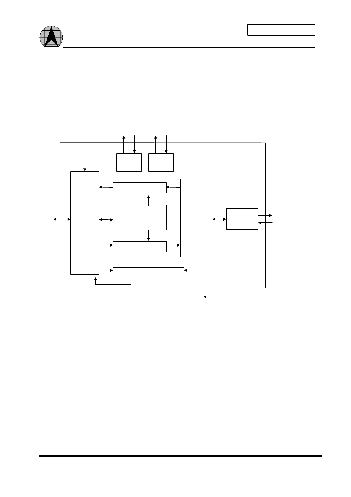
1.3 Block Diagram:
SERIAL BOOT ROM
ROM Interface
Serial
ROM I/F
PCI MII
BUS
General purpose I/O pins
PCI
BUS
Interface
Receive FIFO
Buffer
Management
DMA Engine
Transmit FIFO
General Purpose REG
BOOT
ROM I/F
MAC
Controller
10/100 MII
Interface
Fig - 1 AX88141 Block Diagram
8
ASIX ELECTRONICS CORPORATION
Page 9

AX88141 PRELIMINARY
CONFIDENTIAL
DEVSEL#
AD_20
C_BE#3
AD_26
INT#
AD_19
AD_25
VDD
VDD
VSS
PME#
VSS
AD_29
REQ#
AD_21
AD_16
GNT#
VSS
IDSEL
AD_23
VSS
PCI_CLK
AD_28
VSS
AD_17
VDD
AD_27
AD_30
VDD
AD_18
RST#
VSS
AD_22
AD_24
AD_31
C_BE#2
VSS
PTEST
VSS
1.4 AX88141 Pin Connection Diagram
The AX88141 is housed in the 128-pin plastic quad flat pack. Fig - 2 shows the AX88141 pin
connection diagram.
AD_0
BR_A12
BR_A11
BR_A10
BR_A13
BR_A9
BR_A8
BR_A7
BR_A6
BR_A5
BR_A4
BR_A3
BR_A2
BR_A1
BR_D7
BR_A0
VSS
BR_D6
BR_D5
BR_D4
BR_D3
BR_D2
BR_D1
SR_DI
VDD
SR_CS
VDD
SR_CK
BR_CE#
VSS
AD_1
AD_2
SR_DO/BR_D0
VSS
AD_3
VDD
AD_4
VSS
BR_A14
BR_A15
GEP_0
GEP_1
MDIO
MDC
RXER
VDD
RXDV
VSS
COL
CRS
RXCLK
RXD_0
RXD_1
RXD_2
RXD_3
VDD
TXCLK
VSS
TXEN
TXD_0
TXD_1
VDD
TXD_2
TXD_3
103
104
105
106
107
108
109
110
111
112
113
114
115
116
117
118
119
120
121
122
123
124
125
126
127
128
102
1
101
2
100
3
78
75
77
84
829181
93
94
95
96
989799
90
86
87
8892858983
79
80
76
74
AX88141
8
7
4
6
5
9
10
11
12
13
14
15
16
17
18
19
20
21
22
23
24
25
26
27
28
29
73
30
72
31
71
32
70
33
69
34
68
35
67
36
66
37
65
38
64
63
62
61
60
59
58
57
56
55
54
53
52
51
50
49
48
47
46
45
44
43
42
41
40
39
AD_5
AD_6
AD_7
C_BE#0
VSS
AD_8
AD_9
AD_10
VDD
AD_11
AD_12
VSS
AD_13
AD_14
AD_15
VSS
C_BE#1
PAR
SERR#
PERR#
VDD
STOP#
TRDY#
IRDY#
FRAME#
Fig - 2 AX88141 Pin connection diagram
9
ASIX ELECTRONICS CORPORATION
Page 10

AX88141 PRELIMINARY
CONFIDENTIAL
2.0 Signal Description
2.1 Signal Descriptions
The following terms describe the AX88141 pin-out:
l Address phase
Address and appropriate bus commands are driven during this cycle.
l Data phase
Data and the appropriate byte enable codes are driven during this cycle.
l #
All pin names with the # suffix are asserted low.
The following abbreviations are used in Tab - 1 PCI interface group Tab - 2 Boot ROM , Serial ROM , General-
purpose signals group ,Tab - 3 MII interface signals group ,Tab - 4 Power pins group..
I Input
O Output
I/O Input /Output
O/D Open Drain
2.2 PCI interface group
SIGNAL TYPE PIN
NUMBER
CBE#<3>
CBE#<2>
CBE#<1>
CBE#<0>
DEVSEL# I/O 42 Device select Is asserted by the target of the current bus access. When the AX88141 is the master of the
FRAME# I/O 39 The FRAME# Signal is driven by the AX88141 To indicate the beginning and duration of an access.
GNT# I 7 BUS GRANT Indicates to the AX88141 That access to the bus is granted.
IDSEL I 22 Initialization devise select asserts To indicate that the host is issuing a configuration cycle to the
INT# O/D 1 Interrupt request asserts When one of the appropriate bits of reg5 sets and causes an interrupt, provided
IRDY# I/O 40
PAR I/O 47 Parity is an even parity bit for the AD<31:0> AD and CBE#<3:0>.
I/O 21,
38,
48,
61
BUS COMMAND and BYTE ENABLE Are multiplexed on the same PCI pins. During the address
phase of the transaction, CBE#<3:0> Provide the BUS COMMAND. During the data phase,
CBE#<3:0> Provide the BYTE ENABLE. The BYTE ENABLE determines which byte lines carry
valid data., CBE#<0> Applies to byte 0, and CBE#<3> Applies to byte 3.
current bus access, the target assert DEVSEL# confirming the access. It is driven by AX88141 When
AX88141 is selected as a slave.
FRAME# Asserts to indicate the beginning of a bus transaction. While FRAME# is asserted, data
transfers continue. When FRAME# deasserts the next data phase is the final data phase transaction.
AX88141.
that the corresponding mask bit in reg7 is not asserted. interrupt request deasserts by writing a 1 into the
appropriate reg5 bit.
This pin must be pulled up by an external resistor.
Initiator ready Indicates the bus master ability to complete the current data phase of the transaction.
A data phase is completed on any rising edge of the clock When both IRDY# and target ready TRDY#
are asserted. Wait cycles are inserted until both IRDY# and TRDY# are asserted together.
When the AX88141 is the bus master, IRDY# is asserted during write operations to indicate that valid
data is present on the AD<31:0>. During read operations, the AX88141 asserts IRDY# to indicate that
it is ready to accept data.
During address and data phases, parity is calculated on all the AD<31:0> AND CBE#<3:0>lines
whether or not any of these lines carry meaningful information.
DESCRIPTION
10
ASIX ELECTRONICS CORPORATION
Page 11

AX88141 PRELIMINARY
CONFIDENTIAL
AD<31>
AD<30>
AD<29>
AD<28>
AD<27>
AD<26>
AD<25>
AD<24>
AD<23>
AD<22>
AD<21>
AD<20>
AD<19>
AD<18>
AD<17>
AD<16>
AD<15>
AD<14>
AD<13>
AD<12>
AD<11>
AD<10>
AD<9>
AD<8>
AD<7>
AD<6>
AD<5>
AD<4>
AD<3>
AD<2>
AD<1>
AD<0>
PCI_CLK I 5 The clock provides the timing for the AX88141 related PCI bus transactions. All the bus signals are
PERR# I/O 45 Parity error asserts when a data parity error is detected. When the AX88141 is the bus master it monitor
REQ# O 8 Bus request is asserted by the AX88141 to indicate to the bus arbiter that it wants to use the bus.
RST# I 2 Resets the AX88141 to its initial state. This signal must be asserted for at least 10 active PCI clock
SERR# I/O 46 System Error is used by AX88141 to report address parity Error. This pin must be pulled up by an
STOP# I/O 43 Stop indicator indicates that the current target is requesting the bus master to stop the current transaction.
TRDY# I/O 41 Target ready indicates the target ability to complete the current data phase of the transaction.
PME# O 9
I/O 10,
11,
13,
14,
16,
17,
19,
20,
24,
25,
26,
27,
29,
30,
33,
34,
50,
51,
52,
54,
55,
57,
58,
59,
62,
63,
64,
66,
67,
69,
70,
72
Address and data bits are multiplexed on the same pins. During the address phase, the AD<31:0>
contain a physical address (32 bits). During, data phases, AD<31:0> contain 32 bits of data.
The AX88141 supports both read and write bursts (in master operation only). Little and big endian byte
ordering can be used.
sampled on the rising edge of PCI_CLK. The clock frequency range is between 20MHZ and 33MHZ.
PERR# to see if the target report a data parity error., when the AX88141 is the bus target and a parity
error is detected, the AX88141 asserts PERR#. This pin must be pulled up by an external resistor.
cycles. When is the reset state, all PCI output pins are put into tri-state and all PCI o/d signals are
floated.
external resistor.
The AX88141 responds to the assertion of STOP# when it is the bus master, and stop the current
transaction.
A data phase is completed on any clock when both TRDY# and IRDY# are asserted. Wait cycles are
inserted until both IRDY# and TRDY# are asserted together. When the AX88141 is the bus master,
target ready is asserted by the bus slave on the read operation, indicating that valid data is present on the
ad lines. During a write cycle, it indicates that the target is prepared to accept data.
2.3 Boot ROM , Serial ROM , General-purpose signals group
SIGNAL TYPE PIN
NUMBER
Tab - 1 PCI interface group
DESCRIPTION
11
ASIX ELECTRONICS CORPORATION
Page 12

AX88141 PRELIMINARY
CONFIDENTIAL
BR_A<15>
BR_A<14>
BR_A<13>
BR_A<12>
BR_A<11>
BR_A<10>
BR_A<9>
BR_A<8>
BR_A<7>
BR_A<6>
BR_A<5>
BR_A<4>
BR_A<3>
BR_A<2>
BR_A<1>
BR_A<0>
BR_D<7>
BR_D<6>
BR_D<5>
BR_D<4>
BR_D<3>
BR_D<2>
BR_D<1>
BR_D<0>/
SR_DO
BR_CE# O 78 Boot ROM chip enable.
SR_CK O 76 Serial ROM clock signal.
SR_CS O 77 Serial ROM chip-select signal.
SR_DI O 79 Serial ROM data-in signal.
GENP<1>
GENP<0>
O 104,
103,
102,
101,
100,
99,
98,
97,
96,
95,
94,
93,
92,
91,
90,
89
I 88,
86,
85,
84,
83,
82,
81,
73
I/O 106,
105
Boot ROM address lines bit 15 to bit 0.
Boot ROM data lines bit 7 to bit 0.
Serial ROM data-out signal.
General-purpose pins can be used by software as either status pins or control pins. These pins can be
configured by software to perform either input or output functions.
Tab - 2 Boot ROM , Serial ROM , General-purpose signals group
2.4 MII interface signals group
SIGNAL TYPE PIN
NUMBER
FOR 160 PIN
COL I 113 Collision detected is asserted when detected by an external physical layer protocol(PHY)
CRS I 114 Carrier sense is asserted by the PHY when the media is active.
RXDV I 111 Data valid is asserted by an external PHY when receive data is present on the RXD lines
RXER I 109 Receive error asserts when a data decoding error is detected by an external PHY device.
MDC O 108 MII management data clock is sourced by the AX88141 to the PHY devices as a timing
MDIO I/O 107 MII management data input/output transfers control information and status between the
RXCLK I 115 Supports either the 25-MHZ or 2.5-MHZ receive clock. This clock is recovered by the
RXD<3>
RXD<2>
RXD<1>
RXD<0>
TXCLK I 121 Supports the 25-MHZ or 2.5-MHZ transmit clock supplied by the external physical layer
TXD<3>
TXD<2>
TXD<1>
TXD<0>
TXEN O 123 Transmit enable signals that the transmit is active to an external PHY device.
I 119,
118,
117,
116
O 128,
127,
125,
124
device.
and is deasserted at the end of the packet. This signal should be synchronized with the
RXCLK signal.
This signal is synchronized to RXCLK and can be asserted for a minimum of one receive
clock. When asserted during a packet reception, it sets the cyclic redundancy check(CRC)
error bit in the receive descriptor (RDESO).
reference for the transfer of information on the MII_MDIO signal.
PHY and the AX88141.
PHY.
Four parallel receive data lines When MII mode is selected. This data is driven by an
external PHY that attached the media and should be synchronized with the RXCLK signal.
medium dependent (PMD) device. This clock should always be active.
Four parallel transmit data lines. This data is synchronized to the assertion of the TXCLK
signal and is latched by the external PHY on the rising edge of the TXCLK signal.
DESCRIPTION
Tab - 3 MII interface signals group
12
ASIX ELECTRONICS CORPORATION
Page 13

AX88141 PRELIMINARY
CONFIDENTIAL
2.5 Power pins group
SIGNAL TYPE PIN
NUMBER
VDD P 3,18,28,31,44,56,
68,75,80,110,120,
126
VSS P 4,6,12,15,23,32,
35,37,49,53,60,
65,71,74,87,112,
122
DESCRIPTION
5-V supply input voltage.
Ground pins.
Tab - 4 Power pins group
13
ASIX ELECTRONICS CORPORATION
Page 14

AX88141 PRELIMINARY
CONFIDENTIAL
3.0 Configuration Operation
1. Software reset (REG0<0>) has no effect on the configuration registers.
2. Hardware reset puts the configuration registers in default values.
3. The configuration registers could be accessed in byte, word , and long-word.
3.1 Configuration Space Mapping
CONFIGURATION REGISTER IDENTIFIER I/O ADDRESS OFFSET
DEVICE/VENDOR ID CSID 00H
COMMAND AND STATUS CSCS 04H
REVISION CSRV 08H
LATENCY TIMER CSLT 0CH
BASE I/O ADDRESS CBIO 10H
BASE MEMORY ADDRESS CBMA 14H
RESERVED - 18H-28H
SUBSYSTEM/SUBVENDOR ID SSID 2CH
EXPANSION ROM BASE ADDRESS CBER 30H
NEW CAPABILITIES POINTER CNCP 34H
RESERVED - 38H
INTERRUPT CSIT 3CH
SPECIAL USE SUD 40H
POWER MANAGEMENT CPMR 44H - 49H
Tab - 5 Configuration Space Mapping
14
ASIX ELECTRONICS CORPORATION
Page 15

AX88141 PRELIMINARY
CONFIDENTIAL
3.2 Configuration Space
3.2.1 Configuration ID Register (CSID)
FIELD R/W DESCRIPTION
31:16 R Device ID :
15:0 R Vender ID :
3.2.2 Command and Status Configuration Register (CSCS)
FIELD R/W TYPE DESCRIPTION
31 R STATUS Detected Parity Error : active high
30 R STATUS Signal System Error : active high
29 R STATUS Received Master Abort : active high
28 R STATUS Received Target Abort : active high
26:25 R STATUS Device Select Timing : fixed at 01 which indicates a medium assertion of DEVSEL#
24 R STATUS Data Parity Report : active high
23 R STATUS Fast Back-to-Back : always set
22:21 - RESERVED
20 R STATUS Cpapbility of Power Management : always set.
19-9 - RESERVED
8 R/W COMMAND System Error Enable : active high
6 R/W COMMAND Parity Error Response : active high
2 R/W COMMAND Master Operation : active high
1 R/W COMMAND Memory Space Access : active high
0 R/W COMMAND I/O Space Access : Active high
Provides the unique AX88141 ID number (1400H)
Provides the manufacturer of the AX88141 (125BH)
Tab - 6 CSID Configuration ID Register Description
Tab - 7 CSCS Command and Status Configuration Register
3.2.3 Configuration Revision Register (CSRV)
FIELD R/W DESCRIPTION
31:24 R Base Class : Always equal to 2H that indicates the network controller
23:16 R Subclass : Always equal to 0H that indicates the fast Ethernet controller
7:4 R Revision Number : Indicates the AX88141 revision number and is equal to 1H
3:0 R Step Number : Indicates the AX88141 step number and is referred to current silicon step.
Tab - 8 CSRV Configuration Revision Register Description
3.2.4 Configuration Latency Timer Register (CSLT)
FIELD R/W DESCRIPTION
31:16 R/W Reserved
15:8 R/W Configuration Latency Timer. The value after hardware reset equal to 0h.
7:0 R/W Reserved
Tab - 9 CSLT Configuration ID Register Description
15
ASIX ELECTRONICS CORPORATION
Page 16

AX88141 PRELIMINARY
CONFIDENTIAL
3.2.5 Configuration Base I/O Address Register (CBIO)
FIELD R/W DESCRIPTION
31:7 R/W Configuration Base I/O Address : Defines the address assignment mapping of AX88141‘s regs.
6:1 R This field value is 0 when read
0 R I/O Space Indicator : Determines that the register maps into the I/O space. The value in this field is 1.
Tab - 10 CBIO Configuration Base I/O Address Register Description
3.2.6 Configuration Base Memory Address Register (CBMA)
FIELD R/W DESCRIPTION
31:7 R/W Configuration Base Memory Address : Defines the address assignment mapping of AX88141‘s regs.
6:1 R This field value is 0 when read
0 R Memory Space Indicator : Determines that the register maps into the memory space. The value in this field is 0.
Tab - 11 CBMA Configuration Base Memory Address Register Description
3.2.7 Expansion ROM Base Address Register (CBER)
FIELD R/W DESCRIPTION
31:10 R/W Expansion ROM Base Address
9:1 R This field value is 0 when read
0 R/W Expansion ROM Enable Bit : Active high
Tab - 12 CBER Expansion ROM Base Address Register Description
3.2.8 Configuration Interrupt Register (CSIT)
FIELD R/W DESCRIPTION
31:24 R MAX_LAT : time unit is equal to 0.25 microsecond.(28H)
23:16 R MIN_GNT : Time unit is equal to 0.25 microsecond.(14H)
15:8 R Interrupt Pin : The AX88141 uses INTA# and the read value is (01H).
7:0 R/W Interrupt Line : The BIOS writes the routing information into this field.
Tab - 13 CSIT Configuration Interrupt Register Description
3.2.9 Special Use Register (SUD)
FIELD R/W DESCRIPTION
31:30 R Reserved
29 R/W Enable bit, when set to “1”, if GEP LINK pin has transition, PME# will active.
28 R/W This bit will be “1” if GEP LINK pin has transitions.
27 R/W This bit will be “1” if Magic Packet was detected.
26-25 R Reserved
24 R/W Password enable bit, when this bit is set to “1”, AX881401 will check the password from Magic Packet With the stored
23-16 R Reserved
15:8 R/W Driver special Use
7-0 R Reserved
password in REG 0B and REG 1B before asserting the Magic Packet detected bit (<3> of REG 43)
Tab - 14 CSIT Configuration Interrupt Register Description
3.2.10 Subsystem ID and Subsystem Vendor Register (SSID)
FIELD R/W DESCRIPTION
31:16 R Subdsystem ID :
15:0 R Subsystem Vender ID :
Provides the subsystem ID which is loaded from EEPROM at hardware reset
Provides the subsystem vendor ID which is loaded from EEPROM at hardware reset.
16
ASIX ELECTRONICS CORPORATION
Page 17

AX88141 PRELIMINARY
CONFIDENTIAL
Tab - 15 SSID Configuration ID Register Description
3.2.11 New Capabilities Pointer (CNCP)
FIELD R/W DESCRIPTION
7:0 R New Capabilities Pointer :
3.2.12 Power Management register block (Offset 44H to 49H)
OFFSET R/W DESCRIPTION
44H R Capability ID :
45H R Next item pointer :
46H R Power management capabilities, :
47H R Power management capabilities :
48-49H R/W Power management status :
Point to Power management registers starting address, value is 44H
Tab - 16 CNCP Configuration ID Register Description
The value is 01H to indicate power management block.
The value is 00H to indicate this is the last block
The value is 21H to indicate version 1.0 of PCI power management specification and need a device specific initialization
sequence following transition to the DO uninitialized state
The value is 48H to indicate PME# support from Do and D3 hot state.
<15> : PME# status --
Set when the function would normally assert the PME# signal independent of the state of the PME# pin enable
bit. Write a “1” to this bit will clear it and cause the function to stop asserting a PME# (if enabled). Write a “0” no
effect. When reset default is “0”.
<8> : PME# pin enable control bit --
A “1” enable the function to assert PME#. Writing a “0” PME# assertion is disabled. When reset default is “0”
<1:0> : Power state --
Only 00 (D0) and 11 (D3) supported
Tab - 17 CSID Configuration ID Register Description
17
ASIX ELECTRONICS CORPORATION
Page 18

AX88141 PRELIMINARY
CONFIDENTIAL
4.0 Registers Operation
1. The REGs are quad-word aligned, 32-bits long, and must be accessed using long-word
instruction with quad-word aligned addresses only.
2. Reserved bits should be written with 0.; Reserved bits are UNPREDICTABLE on read access.
3. Retries on second data transactions occur in response to burst accesses.
4.1 Registers Mapping
REGISTER MEANING OFFSET FROM REG BASE ADDRESS
(CBIO,CBMA)
REG0 BUS MODE 00H
REG0B MAGIC PACKET PASSWORD LOW <31:0> 04H
REG1 TRANSMIT POLL DEMAND 08H
REG1B MAGIC PACKET PASSWORD HIGH <47:32> 0CH
REG2 RECEIVE POLL DEMAND 10H
REG3 RECEIVE LIST BASE ADDRESS 18H
REG4 TRANSMIT LIST BASE ADDRESS 20H
REG5 STATUS 28H
REG6 OPERATION MODE 30H
REG7 INTERRUPT ENABLE 38H
REG8 MISSED FRAME AND OVERFLOW COUNTER 40H
REG9 SERIAL ROM, AND MII MANAGEMENT 48H
REG10 - 50H
REG11 GENERAL-PURPOSE TIMER 58H
REG12 GENERAL-PURPOSE PORT 60H
REG13 FILTERING BUFFER INDEX 68H
REG14 FILTERING BUFFER DATA 70H
REG14B RESERVED 74H
REG15 RESERVED 78H
REG15B RESERVED 7CH
Tab - 18 Command and Status Register Mapping
18
ASIX ELECTRONICS CORPORATION
Page 19

AX88141 PRELIMINARY
CONFIDENTIAL
4.2 Host REGs
4.2.1 Bus Mode Register (REG0)
FIELD R/W/C DESCRIPTION
31:22 - RESERVED
21 R/W RML - Read Multiple
20 R/W DBO - Descriptor Byte Ordering Mode
19:14 - Reserved.--Written as “0” for future compatibility concern.
13:8 R/W PBL - Programmable Burst Length
7 R/W BLE - Big/Little Endian
6:2 - RESERVED
1 R/W BAR - Bus Arbitration
0 R/W SWR - Software Reset
When set, the AX88141 supports the memory-read-multiple command on the PCI bus. This bus command is used in
memory read bursts with more than one longword. When reset, the AX88141 uses memory-read command in all its
memory read accesses on the PCI bus.
When set, the AX88141 operates in big edian ordering mode for descriptors only.
When reset, the AX88141 operates in little endian mode.
Indicates the maximum number of longwords to be transfered in one DMA transaction. If reset, the AX88141 burst is
limited only by the amount of data stored in the receive FIFO (at least 16 longword), or by the amount of free space in
the transmit FIFO (at least 16 longword) before issuing a bus request. The PBL can be programmed with permissible
values 0,1,2,4,8,16, or 32. After reset, the PBL default value is 0.
When set, the AX88141 operates in big endian byte ordering mode. When reset, the AX88141 operates in little endian
byte ordering mode. Big endian is applicable only for data buffer
Selects the internal bus arbitration between the receive and transmit processes.
When set, a round robin arbitration scheme is applied resulting in equal sharing between processes. When reset, the
receive process has priority over the transmit process, unless the AX88141 is currently transmitting.
When set, the AX88141 resets all internal hardware with the exception of the configuration area and also, it does not
change the port select setting (REG6<18>).
Software reset does not affect the configuration area.
Tab - 19 REG0 Bus Mode Register Description
4.2.2 Magic Packet Password Low (REG0B)
FIELD R/W DESCRIPTION
31:0 R/W MPPL - Magic Packet Password Low
This register contains the magic packet password bits 31 to 0.
Tab - 20 REG1 Transmit Poll Demand Register Description
4.2.3 Transmit Poll Demand (REG1)
FIELD R/W DESCRIPTION
31:0 W TPD - Transmit Poll Demand
When written with any value, the AX88141 checks for frames to be transmitted. If no descriptor is available, the transmit
process returns to the suspended states and REG5<2> is asserted. If the descriptor is available the transmit process resumes.
Tab - 21 REG1 Transmit Poll Demand Register Description
4.2.4 Magic Packet Password High (REG1B)
FIELD R/W DESCRIPTION
31:16 R Reserved
15:0 R/W MPPH - Magic Packet Password High
This register contains the magic packet password bits 47 to 32.
Tab - 22 REG1 Transmit Poll Demand Register Description
19
ASIX ELECTRONICS CORPORATION
Page 20

AX88141 PRELIMINARY
CONFIDENTIAL
4.2.5 Receive Poll Demand (REG2)
FIELD R/W/C DESCRIPTION
31:0 W RPD - Receive Poll Demand
4.2.6 Receive List Base Address (REG3)
1. The register is used to point the AX88141 to the start of receive descriptors list.
2. The descriptor list resides in physical memory space and must be longword aligned. The
AX88141 behaves UNPREDICTABLY when the list are not longword aligned.
3. Writing to REG3 is permitted only when receive process is in the stopped state. That is, the
REG3 must be written before the receive START command is given .
When written with any value, the AX88141 checks for receive descriptors to be required. If no descriptor is available,
the receive process returns to the suspended states and REG5<7> is not asserted. If the descriptor is available the receive
process resumes.
Tab - 23 REG2 Receive Poll Demand Register Description
REG3 Receive List Base Address Register Description
FIELD R/W/C DESCRIPTION
31:2 R/W Start of receive list
1:0 R/W Must be 00 for longword alignment
Tab - 24 REG3 Receive List Base Address Register Description
4.2.7 Transmit List Base Address (REG4)
1. The register is used to point the AX88141 to the start of transmit descriptors list.
2. The descriptor list resides in physical memory space and must be long-word aligned. The
AX88141 behaves UNPREDICTABLY when the list are not long-word aligned.
3. Writing to REG4 is permitted only when transmit process is in the stopped state. That is, the
REG4 must be written before the transmit START command is given .
FIELD R/W/C DESCRIPTION
31:2 R/W Start of transmit list
1:0 R/W Must be 00 for long-word alignment
Tab - 25 REG4 Transmit List Base Address Register Description
20
ASIX ELECTRONICS CORPORATION
Page 21

AX88141 PRELIMINARY
CONFIDENTIAL
4.2.8 Status Register (REG5)
1. The status register contains all the status bits that the AX88141 reports to the host.
2. Most of the fields in this register cause the host to be interrupted.
3. REG5 bits are not cleared when read.
4. Writing 1 to these bits clears them; writing 0 has no effect. Each field can be masked.
Field R/W/C Description
31:26 - Reserved
25:23 R EB - Error Bits
22:20 - Reserved.--Written as “0” for future compatibility concern.
19:17 - Reserved.--Written as “0” for future compatibility concern.
16 R
15 R
13 R FBE - Fatal Bus Error
11 R/W/C GTE - General Purpose Timer Expired
10 R/W/C ETI - Early Transmit Interrupt
9 R/W/C RWT - Receive watchdog Time out
8 R/W/C RPS - Receive Process Stopped
7 R/W/C RU - Receive Buffer Unavailable
6 R/W/C RI - Receive Interrupt
5 R/W/C UNF - Transmit Under-flow
(Not generate interrupt)
Indicates the type of error that
caused system error.
Valid only when fatal bus error
REG5<13> is set.
NIS - Normal Interrupt Summary
Only the unmasked bits affect normal interrupt summary REG5<16> bit Normal interrupt summary bit. Its
value is the logical OR of :
CSR5<0> transmit interrupt
CSR5<2> transmit buffer unavailable
CSR5<6> receive interrupt
CSR5<10> Early transmit interrupt
CSR5<11> General-purpose timer expired
AIS - Abnormal Interrupt Summary
Only unmasked bits affect only the abnormal interrupt summary REG5<15> bit.
Abnormal interrupt summary bits. Its value is the logical OR of :
CSR5<1> transmit process stopped
CSR5<3> transmit jabber time out
CSR5<5> transmit under-flow
CSR5<7> receive buffer unavailable
CSR5<8> receive process stopped
CSR5<9> receive watchdog time out
CSR5<13> fatal bus error
Indicates that a system error occurred. If a system error occurs, all bus accesses are disabled
Indicates that the general-purpose timer (REG11) counter has expired. This timer is mainly used by the
software driver.
Indicates that the packet to be transmitted was fully transferred into the chip‘s internal transmit FIFOs.
Transmit interrupt (REG5<0>) automatically clears this bit.
Indicates that the receive watchdog timer expired and another node is still active on the network. In case of
overflow, the long packets may not be received.
Asserts when the receive process enters stopped state.
Indicates the next descriptor in the receive list is owned by the host and cannot be acquired by the
AX88141.The reception process is suspended.
Indicates the completion of a frame reception. Specific frame status information has been posted in the
descriptor. The reception process remains in the running state.
Indicates that the transmit FIFO had an under-flow condition during the packet transmission. The transmit
process is placed in the suspended state and under-flow error TDES0<1> is set.
25 24 23 Description
0 0 0 Parity error
0 0 1 Master abort
0 1 0 Target abort
0 1 1 Reserved
1 x x Reserved
4 - Reserved.--Written as “0” for future compatibility concern.
21
ASIX ELECTRONICS CORPORATION
Page 22

AX88141 PRELIMINARY
CONFIDENTIAL
3 R/W/C TJT - Transmit Jabber Time-out
2 R/W/C TU - Transmit Buffer Unavailable
1 R/W/C TPS - Transmit Process Stopped
0 R/W/C TI - Transmit Interrupt
Indicates that the transmit jabber timer expired, meaning that the AX88141 transmitter had been excessively
active. The transmission process is aborted and placed in the stopped state. This event causes the transmit
jabber time-out TDES0<14> is set.
Indicates that the next descriptor on the transmit list is owned by the host and cannot be acquired by the
AX88141.The transmission process is suspended. To resume processing transmit descriptors, the host should
change the ownership bit of the descriptor and then issue a transmit poll demand command.
Asserts when the transmit process enters the stopped state.
Indicates that a frame transmission was completed, while TDES1<31> is asserted in the first descriptor of the
frame.
Tab - 26 REG5 Status Register Description
4.2.9 Operation Mode Register (REG6)
1. REG6 establishes the receive and transmit operating modes and commands.
2. REG6 should be the last REG to be written as part of initialization.
Field R/W/C Description
31 - Reserved
29:23 - Reserved.--Written as “0” for future compatibility concern.
20 - Reserved.--Written as “0” for future compatibility concern.
17:16 - Reserved.--Written as “0” for future compatibility concern.
15:14 R/W
11:10 R/W OM - Operating Mode
6 R/W PR - Promiscuous Mode 1 Indicates that any incoming valid frame is received, regardless
TR - Threshold Control Bits
The threshold value has a direct impact on the AX88141 bus arbitration scheme . Transmission starts when the frame size
within the transmit FIFO is larger than the threshold. In addition, full frames with a length less than the threshold are also
transmitted. The transmit process must be in the stopped state to change these bits.
Controls the selected threshold level for the AX88141 transmit FIFO. Four threshold levels are allowed.
REG6<18>=0 REG6<18>=1 REG6<18>=1
REG6<21> REG6<15:14> REG6<22>=X REG6<22>=1 REG6<22>=0
0 00 72 72 128
0 01 96 96 256
0 10 128 128 512
0 11 160 160 1024
1 XX Store & Forward Store & Forward Store & Forward
1 All incoming packets will be received30 R/W RA - Receive All
0 Filtering mode
1 Threshold is 10Mb/s22 R/W TTM - Transmit Threshold Mode
0 Threshold is 100Mb/s
1 Enable Store and Forward21 R/W SF - Store and Forward
0 Disable Store and Forward
1 Heartbeat Disable19 R/W HBD - Heartbeat Disable
0 Heartbeat Enable
1 MII port is selected.18 R/W PS - Port Select
0 N/A
1 Start Transmission13 R/W ST - Start/Stop Transmission
0 Stop Transmission
1 Enable force collision12 R/W FC - Force Collision Mode
0 Disable force collision
00 Normal
01 Internal Loop-back
10 External Loop-back
1 Full-Duplex9 R/W FD - Full-Duplex Mode
0 Half-Duplex
1 Accept broadcast packet8 R/W RB - Receive broadcast packet
0 Reject broadcast packet
1 Enable Pass All Multicast7 R/W PM - Pass All Multicast
0 Disable Pass All Multicast
22
of its destination address.
ASIX ELECTRONICS CORPORATION
Page 23

AX88141 PRELIMINARY
CONFIDENTIAL
5:4 - Reserved.--Written as “0” for future compatibility concern.
3 R/W PB - Pass Bad Frames
2 - Reserved.--Written as “0” for future compatibility concern.
0 Disable Promiscuous Mode.
1 All incoming frames that passed the address filtering are
received, including runt frames, collided fragments, or
truncated frames caused by FIFO over-flow. If any received bad
frames are required, promiscuous mode (REG6<6>) should be
set to 1.
0 Disable pass bad frame.
1 Start Receive1 R/W SR - Start/Stop Receive
0 Stop Receive
1 AX88141 Mode.0 R/W FIFO Mode
0 AX88140 Mode.
Tab - 27 REG6 Operation Mode Register Description
Port and Data Rate Selection
REG6
<18>
REG6
<22>
1 1 MII 10MB/S MII with transmit FIFO thresholds appropriate for 10MB/S
1 0 MII 100MB/S MII with transmit FIFO thresholds appropriate for 100MB/S
ACTIVE
PORT
DATA
RATE
FUNCTION
Tab - 28 Port and Data Rate Selection
23
ASIX ELECTRONICS CORPORATION
Page 24

AX88141 PRELIMINARY
CONFIDENTIAL
4.2.10 Interrupt Enable Register (REG7)
1. The interrupt enable register (REG7) enables the interrupts reported by REG5.
2. Setting bit to 1 enables a corresponding interrupt. After a hardware or software reset, all interrupts are disabled.
Field R/W/C Description
31:17 - Reserved
16 R/W
15 R/W
13 R/W FBE - Fatal Bus Error interrupt enable. Active high.
11 R/W GPT - General purpose Timer interrupt Enable. Active high.
10 R/W ETE - Early Transmit Interrupt Enable. Active high.
9 R/W RW - Receive Watchdog Time out interrupt Enable. Active high
8 R/W RS - Receive Stopped interrupt Enable. Active high.
7 R/W RU - Receive Buffer Unavailable interrupt Enable. Active high.
6 R/W RI - Receive Interrupt Enable. Active high.
5 R/W UN - under-flow interrupt Enable. Active high.
4 - Reserved.--Written as “0” for future compatibility concern.
3 R/W TJ - Transmit Jabber Time out interrupt Enable. Active high.
2 R/W TU - Transmit Buffer Unavailable interrupt Enable. Active high.
1 R/W TS - Transmission Stopped interrupt Enable. Active high.
0 R/W TI - Transmit Interrupt Enable. Active high.
NI - Normal Interrupt Summary Enable
When set, normal interrupt is enabled.
When reset, no normal interrupt is enabled. This bit (REG7<16>) enables the following bits :
CSR5<0> Transmit interrupt
CSR5<2> Transmit buffer unavailable
CSR5<6> Receive interrupt
CSR5<10> Early transmit interrupt
CSR5<11> General-purpose timer expired
AI - Abnormal Interrupt Summary Enable
When set, abnormal interrupt is enabled.
When reset, no abnormal interrupt is enabled. This bit (REG7<15>) enables the following bits :
CSR5<1> transmit process stopped
CSR5<3> transmit jabber time-out
CSR5<5> transmit under-flow
CSR5<7> receive buffer unavailable
CSR5<8> receive process stopped
CSR5<9> receive watchdog time-out
CSR5<11> fatal bus error
Tab - 29 REG7 Interrupt Enable Register Description
4.2.11 Missed Frame and Overflow Flag (REG8)
Field R/W Description
31: 18 - Reserved
17 R/C Overflow Flag
16 : 1 - Reserved
0 R/C Missed Frame Flag
Tab - 30 REG8 Missed Frame and Overflow Counter Description
Indicates the frames discarded because of overflow. The flag clears when read.
Indicates the frames discarded because no host receive descriptors were available. The flag clears when read.
24
ASIX ELECTRONICS CORPORATION
Page 25

AX88141 PRELIMINARY
CONFIDENTIAL
4.2.12 Serial ROM and MII Management Register (REG9)
1. The register provides an interface to the Microwire serial ROM and to the physical layer
protocol (PHY). It selects the device and contains both the commands and data to be read from
and stored in the serial ROM.
2. The MII management selects and operation mode for reading and writing the MII.
FIELD R/W/C DESCRIPTION
31:20 - Reserved.--Written as “0” for future compatibility concern.
19 R MDI - MII management data_in
18 R/W MII - MII management operation mode
17 R/W MDO - MII Management write data
16 R/W MDC - MII Management clock
14 R/W RD - Read operation
13:12 - Reserved.--Written as “0” for future compatibility concern.
11 R/W SR - SERIAL ROM select
10:4 - Reserved.--Written as “0” for future compatibility concern.
3 R/W SDO - SERIAL ROM data_out
2 R SDI - SERIAL ROM data_in
Used by the AX88141 to read data from the PHY
Defines the operation mode (read or write) of the PHY.
Specifies the value of the data that AX88141 writes to the PHY
MII management data clock (MII_MDC) is an output signal to the PHY. it is used as a timing reference.
Read control bit. When set together with REG9<12>, The AX88141 performs read cycles from the BOOT ROM, and
the serial ROM.
When set together with either SERIAL ROM read operation (REG9<14>) or SERIAL ROM Write operation
(REG9<13>), The AX88141 selects the SERIAL ROM.
SERIAL ROM data output(SR_DO) From the SERIAL ROM device to the AX88141.
SERIAL ROM Data input(SR_DI) To the SERIAL ROM device from the AX88141.
1 R/W SCLK - SERIAL ROM serial clock
0 R/W SCS - Serial ROM Chip Select
Serial clock (SR_CK) Output to the SERIAL ROM.
Chip select (sr_cs) output to the serial ROM.
Tab - 31 REG9 Serial ROM, and MII Management Register Description
4.2.13 General -Purpose Timer (REG11)
1. This register contains a 16 bit general-purpose timer. It is used mainly by the software driver for
timing functions not supplied by the operating system. After the timer is loaded, it starts
counting down . The expiration of the timer causes an interrupt in REG5<11>.
2. If the timer expires with the CON bit on, the counter will load itself automatically with the last
value. The timer is not active in snooze mode.
Field R/W/C Description
31:17 - Reserved.--Written as “0” for future compatibility concern.
15:0 R/W Timer value
Contains the general-purpose timer value within a N microsecond cycle.
SRL_10M : 204.8us
MII_10M : 819.2us
MII_100M : 81.92us
1 Continuous operating mode.16 R/W CON - Continuous Mode
0 One-shot operating mode.
25
ASIX ELECTRONICS CORPORATION
Page 26

AX88141 PRELIMINARY
CONFIDENTIAL
Tab - 32 REG11 General -Purpose Timer Register Description
4.2.14 General -Purpose Port Register (REG12)
Field R/W/C Description
31:9 - Reserved.--Written as “0” for future compatibility concern.
8 R/W GPC - General Purpose Control .
When a hardware reset is initiated, all gep pins
become input pins.
7:0 R/W MD - General Purpose Mode and Data
Tab - 33 REG12 General -Purpose Port Register Description
4.2.15 Filtering Index (REG13)
FIELD R/W/C DESCRIPTION
31:6 - Reserved.--Written as “0” for future compatibility concern.
5:0 R/W FI - Filtering Index
When writing data to filtering buffer, uses filtering index register REG13 to point the position (buffer number) in
filtering buffer. The valid value is between 0 and 3.
Tab - 34 REG13 Filtering Index Register Description
1 Indicate next write REG12<7:0> is use for define
General purpose port in/out direction.
0 Indicate next write REG12<7:0> is use for read/write
general purpose port data.
4.2.16 Filtering data (REG14)
FIELD R/W/C DESCRIPTION
31:0 R/W FD - Filtering Data
By indexed by filtering index register REG13, write the filtering data register REG14 to put filtering address/hash table
into filtering buffer..
Tab - 35 REG14 Filtering Data Register Description
Filtering Buffer
The AX88141 stores one Ethernet address for local physical address and filters the packets
with multicast addresses by 64 bits array. For any incoming frame with a multicast destination
address, the AX88141 applies the standard Ethernet cyclic redundancy check function to the
destination address, then uses the most significant 6 bits of the result as a bit index into the table. If
the indexed bit is set, the frame is accepted. If the bit is reset, the frame is rejected.
Description of Filtering Buffer
BUFFER
NUMBER
0 BYTE 0 - 3 OF LOCAL PHYSICAL ADDRESS
1 BYTE 4 - 5 OF LOCAL PHYSICAL ADDRESS IN THE LEAST SIGNIFICANT WORD
2 BIT 0 - 31 OF MULTICAST ADDRESS FILTERING TABLE
3 Bit 32 - 63 of multicast address filtering table
Tab - 36 Description of Filtering Buffer
DESCRIPTION
Layout of Filtering Buffer
BUFFER
NUMBER
BYTE 3 BYTE 2 BYTE 1 BYTE 0
0 PHYSICAL ADDRESS
BYTE 3
PHYSICAL ADDRESS
BYTE 2
26
PHYSICAL ADDRESS
BYTE 1
ASIX ELECTRONICS CORPORATION
PHYSICAL ADDRESS BYTE 0
Page 27

AX88141 PRELIMINARY
CONFIDENTIAL
1 RESERVED RESERVED PHYSICAL ADDRESS
2
3
MULTICAST
ADDRESS
FILTERING TABLE
BIT 24 - 31
multicast address
filtering table bit 56 - 63
MULTICAST
ADDRESS
FILTERING TABLE
BIT 16 - 23
multicast address
filtering table bit 48 - 55
BYTE 5
MULTICAST ADDRESS
FILTERING TABLE BIT
8 - 15
multicast address filtering
table bit 40 - 47
Tab - 37 Layout of Filtering Buffer
PHYSICAL ADDRESS BYTE 4
MULTICAST ADDRESS FILTERING
TABLE BIT 0 - 7
multicast address filtering table bit 32 -
39
27
ASIX ELECTRONICS CORPORATION
Page 28

AX88141 PRELIMINARY
CONFIDENTIAL
5.0 Host Communication
Descriptor lists and data buffers, collectively called the host communication, reside in the host
memory and manage the actions and status related to buffer management.
5.1 Descriptor Lists and Data Buffers
The AX88141 transfers data frames to the receive buffers and from the transmit buffers in host
memory. Descriptors that reside in the host memory act as pointers to these buffers.
There are two descriptor lists, one for receive and one for transmit. The base address of each list is
written into REG3 and REG4, respectively. A descriptor list is forward-linked (explicitly). The last
descriptor may point back to the first entry to create a ring structure. Explicit chaining of descriptors
is accomplished by setting the address pointer chained in both the receive and transmit descriptors
(RDES3 and TDES3). The descriptor lists reside in the host physical memory address space.
A data buffer consists of either an entire frame or part of a frame, but it cannot exceed a single
frame. Buffers contain only data; buffer status is maintained in the descriptor. Data chaining refers
to frames that span multiple data buffers.
Descriptor Structure Example
Descriptor 0
Descriptor 1
Next Descriptor
Fig - 3 Descriptor Structure Example
Buffer 1
Buffer 2
28
ASIX ELECTRONICS CORPORATION
Page 29

AX88141 PRELIMINARY
CONFIDENTIAL
5.2 Receive Descriptors
The receive descriptor provides one buffer, one byte-count buffer, and one address pointer in
each descriptor. Descriptors and receive buffers addresses must be long-word aligned.
Receive Descriptor Format
31 0
O
RDES0
RDES1 Control bits Byte Count Buffer 2 Byte Count Buffer 1
RDES2 Buffer Address 1
RDES3 Buffer Address 2
W
Status
N
Fig - 4 Receive Descriptor Format
5.2.1 Receive Descriptor 0 (RDES0)
RDES0 contains the received frame status, the frame length, and the descriptor ownership
information.
Field Description
The AX88141 clears this bit either when it completes the
frame reception or
when the buffers that are associated with this descriptor are
full.
This bit can be set only when receive all (REG6<30>) is set.
29:16 FL - Frame Length
13:12 Reserved.--Written as “0” for future compatibility concern.
Indicates the length in bytes of the received frame including the cyclic redundancy check (CRC).
This field is valid only when last descriptor (RDES0<8>) is set and descriptor error ( RDES0<14>) is reset.
ES - Error Summary
15
Indicates the logical OR of the following RDES0 bits :
This field is valid only when last descriptor (RDES0<8>) is set.
RDES0<1> CRC error
RDES0<6> collision seen
RDES0<7> frame too long
RDES0<11> runt frame
RDES0<14> descriptor error
14 DE - Descriptor Error. The frame is truncated. Active high.
This field is valid only when last descriptor (RDES0<8>) is set.
1 Indicates that the descriptor is owned by the AX8814131 OWN - Own Bit
0 Indicates that the descriptor is owned by the host
1 Indicates that the frame failed the address recognition filtering30 FF - Filtering Fail
0 Indicates that the frame passed the address recognition filtering
11 RF - Runt Frame. Indicates that this frame is a runt frame. Active high.
This field is valid only when last descriptor (RDES0<8>) is set .
29
ASIX ELECTRONICS CORPORATION
Page 30

AX88141 PRELIMINARY
CONFIDENTIAL
10 MF - Multicast Frame Indicates that this frame is a multicast address.
This field is valid only when last descriptor (RDES0<8>) is set.
1 Indicates that this descriptor contains the first buffer of a frame.9 FS - First Descriptor
0 Indicates that this descriptor is the middle or last buffer of a frame.
1 Indicates that the buffers pointed to by this descriptor, are the last buffers8 LS - Last Descriptor
0 Indicates that this descriptor is the middle or first buffer of a frame.
7 TL - Frame Too Long. Frame length grater then 1518 bytes. Active high.
This field is valid only when last descriptor (RDES0<8>) is set.
6 CS - Collision Seen. This is a late collision.
This field is valid only when last descriptor (RDES0<8>) is set.
5 Reserved.--Written as “0” for future compatibility concern.
4 RW – Received first packet flag after receiver buffer unavailable state is cleared.
3 RE - Report on MII Error. Active high.
2 DB - Dribbling Bit Active high.
If set, and CRC error (RDES0<1>) is reset, then the packet is valid.
1 CE - CRC Error. Active high.
This field is valid only when last descriptor (RDES0<8>) is set.
0 FIFO Overrun. Active high.
Tab - 38 Receive Descriptor 0
5.2.2 Receive Descriptor 1 (RDES1)
FIELD DESCRIPTION
31:11 Reserved.--Written as “0” for future compatibility concern.
10:0 RBS - Receive Data Buffer Size
Indicates the size in bytes of the data buffer. If this field is 0, the AX88141 ignores this buffer.
The buffer size must be a multiple of 4.
Tab - 39 Receive Descriptor 1
5.2.3 Receive Descriptor 2 (RDES2)
FIELD DESCRIPTION
31:0 Data Buffer Pointer
Indicates the physical address of data buffer. The buffer must be long-word-aligned (RDES2<1:0>=00).
Tab - 40 Receive Descriptor 2
5.2.4 Receive Descriptor 3 (RDES3)
FIELD DESCRIPTION
31:0 Address Pointer
Indicates the physical address of next descriptor. The address must be long-word aligned (RDES3<1:0>=00).
Tab - 41 Receive Descriptor 3
30
ASIX ELECTRONICS CORPORATION
Page 31

AX88141 PRELIMINARY
CONFIDENTIAL
5.3 Transmit Descriptors
Providing one buffer, one byte-count buffer, and two address pointers in each descriptor .
Transmit Descriptor Format
31 0
O
TDES0
TDES1 Control bits Byte Count Buffer 2 Byte Count Buffer 1
TDES2 Buffer Address 1
TDES3 Buffer Address 2
W
Status
N
Fig - 5 Transmit Descriptor Format
5.3.1 Transmit Descriptor 0 (TDES0)
TDES0 contains transmitted frame status and descriptor ownership information.
Field Description
1 Indicates that the descriptor is owned by the AX88141.31 OWN - Own Bit
0 Indicates that the descriptor is owned by the host.
30:16 Reserved.--Written as “0” for future compatibility concern.
15
14 TO - Transmit Jabber Time-out : Active high.
13:12 Reserved.--Written as “0” for future compatibility concern.
11 LO - Loss of Carrier during transmission. Active high. (The status is no meaning except 10BASE SRL mode)
10 NC - No Carrier. Indicates that the carrier signal from the transceiver was not present during transmission. Active high.
9 LC - Late Collision. When set, indicates that the frame transmission was aborted due to collision occurring after the collision
8 EC - Excessive Collision When set, indicates that the transmission was aborted after 16 successive collisions while attempting to
7 HF - Heartbeat Fail
6:3 CC - Collision Count
2 Reserved.--Written as “0” for future compatibility concern.
ES - Error Summary
Indicates the logical OR of the following bits :
TDES0<1> under-flow error
TDES0<8> successive collisions
TDES0<9> late collision
TDES0<10> no carrier
TDES0<11> loss of carrier
TDES0<14> transmit jabber time-out
The transmission process is aborted and placed in the STOPPED state.
When TDES0<14> is set any heartbeat fail indication (TDES0<7>) is not valid.
Not valid in internal loop-back mode (REG6<11:10>=01).
Not valid in internal loop-back mode (REG6<11:10>=01).
window of 64 bytes. Not valid if under-flow error (TDES0<1>) is set.
transmit the current frame.
This bit is effective only in 10Mb/s operation mode. When set, indicates a heartbeat collision check failure
This bit is not valid if under-flow error (TDES0<1>) is set.
On the second transmission attempt, after the first transmission was aborted due to collision, the AX88141 does not check
heartbeat fail and (TDES0<7>) is reset.
This 4-bit counter indicates the number of collisions that occurred before the frame was transmitted.
Not valid when the excessive collisions bit (TDES0<8>) is also set.
31
ASIX ELECTRONICS CORPORATION
Page 32

AX88141 PRELIMINARY
CONFIDENTIAL
1 UF - Under-flow Error
When set, indicates that the transmitter aborted the message because data arrived late from memory. Under-flow error indicates
that the AX88141 encountered an empty transmit FIFO while transmitting a frame. The transmission process enters the
suspended state and sets both transmit under-flow (REG5<0>) and transmit interrupt (REG5<0>).
0 DE - Deferred
When set, indicates that the AX88141 had to defer while ready to transmit a frame because the carrier was asserted.
Tab - 42 Transmit Descriptor 0
5.3.2 Transmit Descriptor 1 (TDES1)
Field Description
31 IC - Interrupt on Completion
When set, the AX88141 sets transmit interrupt (REG5<0>) after the present frames has been transmitted. It is valid only when
first segment (TDES1<30>) is set.
28:27 Reserved.--Written as “0” for future compatibility concern.
26 AC - Add CRC Disable
When set, the AX88141 does not append the CRC to the end of the transmitted frame. This field is valid only when first segment
(TDES1<29>) is set.
25:24 Reserved.--Written as “0” for future compatibility concern.
23 DPD - Disabled Padding
The CRC field is added despite the state of
the add CRC disable (TDES1<26>) flag.
1 Indicates that the buffer contains the last segment of a frame.30 LS - Last Segment
0 Indicates that the buffer contains the first or middle segment of a frame.
1 Indicates that the buffer contains the first segment of a frame.29 FS - First Segment
0 Indicates that the buffer contains the middle or last segment of a frame.
1 the AX88141 does not automatically add a padding field, so a packet
shorter than 64 bytes.
0 The AX88141 automatically adds a padding field and also a CRC field to a
packet shorter than 64 bytes.
22:11 Reserved.--Written as “0” for future compatibility concern.
10:0 Data Buffer Size
Indicates the size, in bytes, of the data buffer. If this field is 0, the AX88141 ignores this buffer.
Tab - 43 Transmit Descriptor 1
5.3.3 Transmit Descriptor 2 (TDES2)
Field Description
31:0 Data Buffer Pointer
Physical address of data buffer. There are no limitations on the buffer address alignment.
Tab - 44 Transmit Descriptor 2
5.3.4 Transmit Descriptor 3 (TDES3)
Field Description
31:0 Address Pointer
Physical address of next descriptor address. There are no limitation on the buffer address alignment.
Tab - 45 Transmit Descriptor 3
32
ASIX ELECTRONICS CORPORATION
Page 33

AX88141 PRELIMINARY
CONFIDENTIAL
6.0 Electrical Specification and Timings
6.1 Absolute Maximum Ratings
Description SYM Min Max Units
Operating Temperature Ta 0 +70
Storage Temperature Ts -55 +150
Supply Voltage Vcc -0.5 +7 V
Input Voltage Vin Vss-0.5 Vdd+0.5 V
Output Voltage Vout Vss-0.5 Vdd+0.5 V
Lead Temperature (soldering 10 seconds maximum) Tl -55 +250
Note : Stress above those listed under Absolute Maximum Ratings may cause permanent damage to the device.
Exposure to Absolute Maximum Ratings conditions for extended period, adversely affect device life and reliability
6.2 General Operation Conditions
Description SYM Min Max Units
Operating Temperature Ta 0 +70
Supply Voltage Vdd +4.75 +5.25 V
°C
°C
°C
°C
6.3 DC Characteristics
(Vdd=4.75V to 5.25V, Vss=0V, Ta=0°C to 70°C)
Description SYM Min Tpy Max Units
Low Input Voltage Vil Vss-0.5 0.8 V
High Input Voltage Vih 2 Vdd+0.5 V
Low Output Voltage Vol - 0.4 V
High Output Voltage Voh 2.4 - V
Input Leakage Current 1 (Note 1) Iil1 - 10 uA
Input Leakage Current 2 (Note 2) Iil1 - 500 uA
Output Leakage Current Iol - 10 uA
Power Consumption ( Sleep ,Note 3 ) Ps 18 mA
Power Consumption ( Idle , Driver Loaded ) Pi 72 mA
Power Consumption ( Heavy Traffic ) Pt 110 mA
Note :
1. All the input pins without pull low or pull high.
2. Those pins had been pull low or pull high.
3. When sleep mode, PCI clock stop / Link on ; If link off, typical is 2.5mA .
33
ASIX ELECTRONICS CORPORATION
Page 34

AX88141 PRELIMINARY
CONFIDENTIAL
6.4 A.C. Timing Characteristics
6.4.1 PCI CLOCK
Symbol Description Min Typ. Max Units
Tcyc CYCLE TIME
Thigh PCI_CLK HIGH TIME
Tlow PCI_CLK LOW TIME
Tr/Tf PCI_CLK SLEW RATE
6.4.2 PCI Timings
PCI_CLK
30 - 45 ns
11 - - ns
11 - - ns
1 - 4 ns
Tval Tval
(max) (min)
OUTPUT
Ton Toff
INPUT
Tsu Th
Symbol Description Min Typ. Max Units
Tval CLK TO SIGNAL VALID DELAY
Ton FLOAT TO ACTIVE DELAY
Toff ACTIVE TO FLOAT DELAY
Tsu INPUT SETUP TIME TO CLK
Th INPUT HOLD TIME FROM CLK
2 - 11 ns
2 - - ns
- - 28 ns
7 - - ns
0 - - ns
6.4.3 Reset Timing
PCI_CLK
RST#
Symbol Description Min Typ. Max Units
Trst Reset pulse width
34
10 - - PCI Clk
ASIX ELECTRONICS CORPORATION
Page 35

AX88141 PRELIMINARY
CONFIDENTIAL
6.4.4 MII Timing
Ttclk Ttch Ttcl
TXCLK
Ttv Tth
TXD<3:0>
TXEN
Trclk Trch Trcl
RXCLK
Trs Trh
RXD<3:0>
RXDV
Trs1
RXER
Symbol Description Min Typ. Max Units
Ttclk Cycle time(100Mbps)
Ttclk Cycle time(10Mbps)
Ttch high time(100Mbps)
Ttch high time(10Mbps)
Trch low time(100Mbps)
Trch low time(10Mbps)
Ttv Clock to data valid
Tth Data output hold time
Trclk Cycle time(100Mbps)
Trclk Cycle time(10Mbps)
Trch high time(100Mbps)
Trch high time(10Mbps)
Trcl low time(100Mbps)
Trcl low time(10Mbps)
Trs data setup time
Trh data hold time
Trs1 RXER data setup time
- 40 - ns
- 400 - ns
14 - 26 ns
140 - 260 ns
14 - 26 ns
140 - 260 ns
- - 20 ns
5 - - ns
- 40 - ns
- 400 - ns
14 - 26 ns
140 - 260 ns
14 - 26 ns
140 - 260 ns
6 - - ns
10 - - ns
10 - - ns
35
ASIX ELECTRONICS CORPORATION
Page 36

AX88141 PRELIMINARY
CONFIDENTIAL
6.4.5 Boot ROM Read Cycles
Boot ROM Byte Read Cycle
BR_D<7:0> data
BR_A<15:0> address
BR_CE#
Boot ROM Dword Read Cycle
BR_D<7:0> data3 data2 data1 data0
BR_A<15:0> addr3 addr2 addr1 addr0
BR_CE#
36
ASIX ELECTRONICS CORPORATION
Page 37

AX88141 PRELIMINARY
CONFIDENTIAL
7.0 Package Information
Hd
D
pin 1
He
E
b
e
A2 A1
L1
L
θ
MILIMETERSYMBOL
MIN. NOM MAX
A1 0.21 0.31 0.41
A2 2.80 2.85 2.90
b 0.15 0.20 0.30
D 13.80 14.00 14.20
E 19.80 20.00 20.20
e 0.50
Hd 17.10 17.20 17.30
He 23.10 23.20 23.30
L 0.70 0.80 0.90
L1 1.60
θ
0 8
37
ASIX ELECTRONICS CORPORATION
Page 38

AX88141 PRELIMINARY
CONFIDENTIAL
APPENDIX A H/W NOTE
A.1 Boot ROM read cycle
ASIX 88141 Boot ROM Byte Read Cycle
BR_D<7:0> data
BR_A<15:0> address
BR_CE#
BR_A0
BR_A1
BR_A2
BR_A3
BR_A4
BR_A5
BR_A6
BR_A7
BR_A8
BR_A9
BR_A10
BR_A11
BR_A12
BR_A13
BR_A14
BR_A15
BR_CE#
GND
27512
A0 Q0
A1 Q1
A2 Q2
A3 Q3
A4 Q4
A5 Q5
A6 Q6
A7 Q7
A8
A9
A10
A11
A12
A13
A14
A15
/CE
/OE
BR_D0
BR_D1
BR_D2
BR_D3
BR_D4
BR_D5
BR_D6
BR_D7
DEC 21140 Boot ROM Byte Read Cycle:
br_ad<7:0> address 7-2 address 15-8 data
br_a1 address 1
br_a0 address 17 address16 address 0
brce#
BRAD0
BRAD1
BRAD2
BRAD3
BRAD4
BRAD5
BRAD6
BRAD7
GND
BRA1
74LS374
D0 Q0
D1 Q1
D2 Q2
D3 Q3
D4 Q4
D5 Q5
D6 Q6
D7 Q7
OC
CLK
A10
A11
A12
A13
A14
A15
GND
BRA0
BRA1
74LS374
A8
D0 Q0
A9
D1 Q1
D2 Q2
D3 Q3
D4 Q4
D5 Q5
D6 Q6
D7 Q7
OC
CLK
/WE
/OE
A2
A3
A4
A5
A6
A7
38
A2
A3
A4
A5
A6
A7
A8
A9
A10
A11
A12
A13
A14
A15
BR_CE
/OE
ASIX ELECTRONICS CORPORATION
27512
A0 Q0
A1 Q1
A2 Q2
A3 Q3
A4 Q4
A5 Q5
A6 Q6
A7 Q7
A8
A9
A10
A11
A12
A13
A14
A15
/CE
/OE
BRAD0
BRAD1
BRAD2
BRAD3
BRAD4
BRAD5
BRAD6
BRAD7
Page 39

AX88141 PRELIMINARY
CONFIDENTIAL
A.2 Power Supply
AX88141 power supply is +5V DC
DEC 21140 power supply is +3.3V DC
A.3 Boundary Scan Test Pins
AX88141 do not support boundary scan test pins
DEC 21140 supports boundary scan test pins
39
ASIX ELECTRONICS CORPORATION
Page 40

AX88141 PRELIMINARY
CONFIDENTIAL
APPENDIX B Function Application
B.1 Application for PCI Interface
Features :
l Direct interface to PCI Bus.
l Support 33 MHz no wait state PCI Bus Interface.
l Powerful on chip buffer management DMA. And PCI Bus master operation reduce CPU
utilization.
l 5 Volt CMOS process.
PCI Interface Schematic:
PCI BUS CONNECTOR AX88141 PCI I/O PINS
AD[31:0]
C/BE[3:0]
PAR
PCI SLOT MAC
FRAME#
TRDY#
IRDY#
STOP#
DEVSEL#
IDSEL
PERR#
SERR#
REQ#
GNT#
CLK
RST#
PME#
The pull high resisters are required for pin REQ#, GNT#, PERR#, and SERR# on MAC for more detail please to
check the schematic.
40
ASIX ELECTRONICS CORPORATION
Page 41

AX88141 PRELIMINARY
CONFIDENTIAL
B.2 Application for Boot ROM Interface
AX88141
Boot ROM Byte Read Cycle
BR_D<7:0> data
BR_A<15:0> address
BR_CE#
BR_A0
BR_A1
BR_A2
BR_A3
BR_A4
BR_A5
BR_A6
BR_A7
BR_A8
BR_A9
BR_A10
BR_A11
BR_A12
BR_A13
BR_A14
BR_A15
BR_CE#
GND
27512
A0 Q0
A1 Q1
A2 Q2
A3 Q3
A4 Q4
A5 Q5
A6 Q6
A7 Q7
A8
A9
A10
A11
A12
A13
A14
A15
/CE
/OE
BR_D0
BR_D1
BR_D2
BR_D3
BR_D4
BR_D5
BR_D6
BR_D7
B.3 Application for Serial ROM Interface
AX88141 Serial ROM Chip Select Serial ROM
Serial ROM Clock
Serial ROM Interface Serial ROM Data In 93C46
Serial ROM Data Out
41
ASIX ELECTRONICS CORPORATION
Page 42

AX88141 PRELIMINARY
CONFIDENTIAL
AX88141
MAC Controller
/M-3X51
ST 6166
X
former
RJ-45
AX88141
MAC Controller
ST 6114
X
former
RJ-45
B.4 Applications
B.4.1 Application for NS DP83843
10BASE-T Transceiver
MII
MII
NS DP83843
PHY
‘
STA
A.N. 4B/5B
Scrambler /
Descrambler
Fig - 6 Application for NS DP83843
B.4.2 Application for LUCENT M-LU6612/M-3X51
10BASE-T Transceiver
MII
MII
LUCENT
M-LU6612
‘
STA
A.N. 4B/5B
Scrambler /
Descrambler
Fig - 7 Application for LUCENT M-LU6612
42
ASIX ELECTRONICS CORPORATION
Page 43

AX88141 PRELIMINARY
CONFIDENTIAL
AX88141
MAC Controller
YCL 20PMT04
X
former
RJ-45
B.4.3 Application for TI XTNETE2101
10BASE-T Transceiver
MII
MII
TI
XTNETE2101
‘
STA
A.N. 4B/5B
Scrambler /
Descrambler
Fig - 8 Application for TI XTNETE2101
43
ASIX ELECTRONICS CORPORATION
 Loading...