

Page 1
ASIX ELECTRONICS CORPORATION Ver. 0.7
4F, NO.8, Hsin ANN Rd., Science-based Industrial Park, Hsin-Chu City, Taiwan, R.O.C.
TEL: 886-3-579-9500
FAX: 886-3-579-9558 http://www.asix.com.tw
AX81190 PCI/CARDBUS/PCMCIA Bus WLAN MAC
802.11b PCI/CARDBUS/PCMCIA Bus WLAN MAC Controller
Document No.: AX81190-07 / V0.7 / MAR. 15 ’03
Features
• Single chip multiple bus WLAN MAC Controller
• IEEE 802.11b wireless LAN (WLAN) Compatible
• Compliant with 802.11b protocol such as DCF,
PCF, WEP, Power management, etc.
• Embedded two 8K * 16 bit SRAMs for Tx and Rx
Packet Buffers
• Compliant with PCI Bus Standard Ver 2.1(slave
mode)/PCMCIA Bus standard.
• Support PCI 16-bit accsee for Registers and 32-bit
accsee for Data
• Support both 1/2/5.5/11 Mbps data rate
• Support both full-duplex (Test) or half-duplex
operation
• Provides an industrial standard interface to
interface with baseband processer and IF/RF chips.
• Support 256 bytes EEPROM (used for saving
Configuration Information and address ID)
• Support automatic loading of MAC ID and Adapter
Configuration from EEPROM on power-on
initialization
• 128-pin TQFP low profile package
• 33/44MHz, 2.5Vcore/3.3V IO operation with 5V
tolerance
*IEEE is a registered trademark of the Institute of Electrical and
Electronic Engineers, Inc.
*All other trademarks and registered trademark are the property of their
respective holder.
Product description
The AX81190 is a high performance multiple bus WLAN MAC Controller. The AX81190 contains a 16 bit PCMCIA
interfaces (32-bit PCI/CARDBUS) to host CPU and compliant with PCMCIA Bus Standard Ver 2.2. The AX81190
implements
1Mbps, 2Mbps, 5.5Mbps and 11Mbps WLAN function based on DSSS (Direct Sequence Spread
Spectrum) of IEEE802.11 /IEEE802.11b WLAN standard. The AX81190 supports an industrial standard(such as Intersil
/RFMD/RaLink) interface for baseband processer and IF/RF chips to simplify the design.
SYSTEM BLOCK DIAGRAM
Always contact ASIX for possible updates before starting a design.
This data sheet contains new products information. ASIX ELECTRONICS reserves the rights to modify product
specification without notice. No liability is assumed as a result of the use of this product. No rights under any patent
accompany the sale of the product.
MAC -- AX81190
RaLink 2430 or
BB -- RFMD R3000 or
RF
PCI/CARDBUS
PCMCIA
Page 2

ASIX ELECTRONICS CORPORATION
2
AX81190 PCI/CARDBUS/PCMCIA Bus WLAN MAC
CONTENTS
1.0 INTRODUCTION ...........................................................................................................6
1.1 GENERAL DESCRIPTION ............................................................................................................6
1.2 AX81190 BLOCK DIAGRAM .................................................................................................6
1.3 AX81190 PIN CONNECTION DIAGRAM.......................................................................7
1.3.1 AX88119 Pin Connection Diagram for PCMCIA Bus Mode ..............................7
1.3.2 AX81190 Pin Connection Diagram for PCI/CardBus Mode...............................8
2.0 SIGNAL DESCRIPTION ...................................................................................9
2.1 PCMCIA BUS INTERFACE SIGNALS GROUP........................................................... 9
2.2 PCI/CARDBUS BUS INTERFACE SIGNALS GROUP .......................................10
2.3 EEPROM SIGNALS GROUP..................................................................................................11
2.4 SERIAL PORT INTERFACE SIGNALS GROUP............................................................11
2.5 BASEBAND PROCESSER CONTROLLER INTERFACE SIGNALS GROUP11
2.6 POWER CONTROL INTERFACE SIGNALS GROUP ................................................12
2.7 SYNTHESIZER CONTROL SIGNAL INTERFACE PINS GROUP ........................12
2.8 MISCELLANEOUS PINS GROUP............................................................................................ 12
3.0 REGISTERS OPERATION .........................................................................14
3.1 PCI CONFIGURATION REGISTER......................................................................................14
3.1.1 Device vendor register -- offset 00h .................................................................................14
3.1.2 Command register – offset 04h ...........................................................................................14
3.1.3 Status register – offset 06h..................................................................................................... 14
3.1.4 Revision ID register – offset 08h........................................................................................14
3.1.5 Class code register – offset 09h.......................................................................................... 15
3.1.6 Base IO address register – offset 10h..............................................................................15
3.1.7 Base Memory address register – offset 14h.................................................................15
3.1.8 CIS pointer – offset 28h ...........................................................................................................15
3.1.9 Subsystem ID – 2Ch................................................................................................................... 15
3.1.10 Interrupt register – 3Ch........................................................................................................15
3.2 PCMCIA CONFIGURATION REGISTER....................................................................... 16
3.2.1 COR register – 0800h............................................................................................................... 16
3.2.2 CCR register – 0802h.............................................................................................................. 16
3.2.3 IO base (LSB) – 0804h............................................................................................................. 16
3.2.4 IO base (MSB) – 0806h............................................................................................................16
3.3 IO PORT..................................................................................................................................................17
3.3.1 CSR index port base................................................................................................17
Page 3

ASIX ELECTRONICS CORPORATION
3
AX81190 PCI/CARDBUS/PCMCIA Bus WLAN MAC
3.3.2 CSR data port base + 2.............................................................................................17
3.3.3 Tx Data access control port base + 4............................................................. 17
3.3.4 Tx data buffer port base + 6............................................................................. 17
3.3.5 Rx Data access control port base + 8............................................................. 17
3.3.6 Rx data buffer port base + ah ...........................................................................17
3.3.7 Soft reset port base + eh .............................................................................................17
3.3.8 Interrupt status port base + 10h ...........................................................................17
3.3.9 Interrupt mask port base + 12h ........................................................................... 18
3.3.10 Rx page status port base + 14h........................................................................18
3.3.11 Tx page status port1 base + 16h .....................................................................18
3.3.12 Tx page status port2 base + 18h .....................................................................19
3.3.13 BBP_index port base + 1ah ............................................................................19
3.3.14 BBP_data out port base + 1ch .........................................................................19
3.3.15 BBP_data in port base + 1eh .............................................................................19
3.3.16 Synthesizer control port base + 20h .............................................................19
3.3.17 Synthesizer data port0 base + 22h.................................................................19
3.3.18 Synthesizer data port1 base + 24h.................................................................19
3.3.19 EE_data port base + 26h..................................................................................20
3.3.20 EE_cmd/addr port base + 28h ...................................................................... 20
3.3.21 EE_status_type port base + 2ah .....................................................................20
3.4 MAC CONFIGURATION STATUS REGISTERS.........................................................21
3.4.1 CSR1 – MAC Physical address0 (PADR[15:0])....................................................... 21
3.4.2 CSR2 – MAC Physical address1 (PADR[31:16])....................................................21
3.4.3 CSR3 – MAC Physical address2 (PADR[47:32])....................................................21
3.4.4 CSR4 – BSSID Matching Register0, BSSID[15:0]..................................................21
3.4.5 CSR5 – BSSID Matching Register1, BSSID[31:16]............................................... 21
3.4.6 CSR6 – BSSID Matching Register2, BSSID[47:32]............................................... 21
3.4.7 CSR7 ~ CSR9 are reserved. .................................................................................................21
3.4.10 CSR10 – Multicast filter pattern1................................................................................... 21
3.4.11 CSR11 – Multicast filter pattern2................................................................................... 21
3.4.12 CSR12 – Multicast filter pattern3................................................................................... 21
3.4.13 CSR13 – Multicast filter pattern4................................................................................... 21
3.4.12 CSR14 ~ CSR15 are reserved. .......................................................................................22
3.4.16 CSR16 – clock pattern.......................................................................................................... 22
3.4.17 CSR17 – Wait md_rdy duration...................................................................................... 22
3.4.18 CSR18 – Short Interframe space timing register ,SIFS.................................... 22
3.4.19 CSR19 – Distributed Interframe space timing register, DIFS/PIFS......... 22
3.4.20 CSR20 ~ CSR 21 – Reserved. ............................................................................................22
3.4.22 CSR22 – SlotTime Register (SLOT) .............................................................................22
3.4.23 CSR23 – Backoff timing........................................................................................................22
3.4.24 CSR24 – RF3000 modulation duration (Testing)..................................................22
3.4.25 CSR25 – Power Testing and misc...................................................................................22
Page 4

ASIX ELECTRONICS CORPORATION
4
AX81190 PCI/CARDBUS/PCMCIA Bus WLAN MAC
3.4.26 CSR26 – TXVGC adjust register (support RF3000 only).................................23
3.4.27 CSR27 – Tx Beacon/probe response enable register ..........................................23
3.4.28 CSR28 – TBTT Compensation Register ......................................................................23
3.4.29 CSR29 – Rx filtering Register ...........................................................................................23
3.4.30 CSR30 – TX Power Ramp-up Control Register1................................................... 24
3.4.31 CSR31 – TX Power Ramp-up Control Register2................................................... 24
3.4.32 CSR32 – TX Power Ramp Control Register3 ..........................................................24
3.4.33 CSR33 – TX Power Ramp Control Register4 ..........................................................24
3.4.34 CSR34 – TX Power Ramp Control Register5 ..........................................................24
3.4.35 CSR35 – BeaconPeriod (BP).............................................................................................24
3.4.36 CSR36 – Tx Retry counter ...................................................................................................24
3.4.37 CSR37 – MAC feature register......................................................................................... 24
3.4.38 CSR38 is Reserved ...................................................................................................................25
3.4.39 CSR39 – Transmit page control register.................................................................... 25
3.4.40 CSR40 – TX Rate control register.................................................................................. 25
3.4.41 CSR41 – response time-out register ..............................................................................26
3.4.42 CSR42 – RSSI-SQ location register...............................................................................26
3.4.43 CSR43 – TSF compensate register................................................................................. 26
3.4.44 CSR44 – Calibration adjust register.............................................................................26
3.4.45 CSR45 – BBP PLCP Service/Signal field location register ( for Intersil
3861/3863)
...................................................................................................................................................26
3.4.46 CSR46 – BBP PLCP Length field location register (for Intersil
3861/3863)
...................................................................................................................................................26
3.4.47 CSR47 is Reserved ...................................................................................................................27
3.4.48 CSR48 – Software reset duration.................................................................................... 27
3.4.49 CSR49 – CFP duration register.......................................................................................27
3.4.50 CSR50 – ATIM duration register ....................................................................................27
3.4.51 CSR51 – 802.11 protocol status.......................................................................................27
3.4.52 CSR52 – MAC mode status................................................................................................. 27
3.4.53 CSR53 – BBP mode.................................................................................................................27
3.4.54 CSR54 – SPI chip address...................................................................................................28
3.4.55 CSR55 ~ CSR59 reserved ................................................................................................... 28
3.4.60 CSR60 CRC32 counter.......................................................................................................... 28
3.4.61 CSR61 is reserved.................................................................................................................... 28
3.4.62 CSR62 – NAV timer.................................................................................................................28
3.4.63 CSR63 – TSF timer register0 (TSFR[15:0]) ............................................................28
3.4.64 CSR64 – TSF timer register1 (TSFR[31:16]).......................................................... 28
3.4.65 CSR65 – TSF timer register2 (TSFR[47:32]).......................................................... 28
3.4.66 CSR66 – TSF timer register3 (TSFR[63:48]).......................................................... 28
3.4.67 CSR67 ~ CSR69 Reserved................................................................................................... 28
3.4.70 CSR70 – Not my unicast frame counter.......................................................................28
3.4.71 CSR71 – broadcast and multicast counter ................................................................29
Page 5

ASIX ELECTRONICS CORPORATION
5
AX81190 PCI/CARDBUS/PCMCIA Bus WLAN MAC
3.4.72 CSR72 – RSSI-SQ value........................................................................................................ 29
3.4.73 CSR73 – Outbuf/Inbuf current page pointer ............................................................29
3.4.74 CSR74: TX Power Ramp-down Control Register1...............................................29
3.4.75 CSR75: TX Power Ramp-down Control Register2...............................................29
3.4.76 CSR76: TX Power Ramp-down Control Register3...............................................29
3.4.77 CSR77: TX Power Ramp-down Control Register4...............................................29
3.4.78 CSR78: RX_PE de-asserted duration........................................................................... 29
3.4.79 CSR79: Min size of RX packet ..........................................................................................30
3.4.80 CSR80: GPIO status control.............................................................................................. 30
3.4.81 CSR81: GPIO data port........................................................................................................ 30
3.4.82 CSR82: wep control ................................................................................................................30
3.4.83 WEP key matrix (csr83 ~ csr110, 16 bit registers)............................................... 30
4.0 PCMCIA DEVICE ACCESS FUNCTIONS.................... 31
4.1 ATTRIBUTE MEMORY ACCESS FUNCTIONS............................................................ 31
4.2 I/O ACCESS FUNCTIONS...........................................................................................................31
5.0 ELECTRICAL SPECIFICATION AND
TIMINGS
.................................................................................................................................................32
5.1 ABSOLUTE MAXIMUM RATINGS...................................................................................... 32
5.2 GENERAL OPERATION CONDITIONS.............................................................................32
5.3 DC CHARACTERISTICS............................................................................................................. 32
5.4 A.C. TIMING CHARACTERISTICS.....................................................................................33
5.4.1 CLOCK.............................................................................................................................................. 33
5.4.2 PCMCIA Reset Timing............................................................................................................. 33
5.4.3 PCMCIA Attribute Memory Read Timing..................................................................... 34
5.4.4 PCMCIA Attribute Memory Write Timing....................................................................35
5.4.5 PCMCIA I/O Read Timing.....................................................................................................36
5.4.6 PCMCIA I/O Write Timing.................................................................................................... 37
5.4.7 Synthesizer Timings.................................................................................................................... 38
5.4.8 Serial Port Timings ....................................................................................................................39
5.4.9 TX Path Waveforms....................................................................................................................40
5.4.10 RX Path Waveforms ................................................................................................................ 41
6.0 PACKAGE INFORMATION....................................................................42
APPENDIX A: APPLICATION NOTE 1........................................ 43
A.1 EXTERNAL EEPROM FORMAT .......................................................................................43
Page 6
ASIX ELECTRONICS CORPORATION
6
AX81190 PCI/CARDBUS/PCMCIA Bus WLAN MAC
1.0 Introduction
1.1 General Description
The AX81190 Wireless LAN Controller is a high performance PCMCIA/PCI bus WLAN Controller. The
AX81190 contains a 16 bit PCMCIA (32 bit PCI) interfaces to host CPU. The AX81190 implement 1Mbps,
2Mbps, 5.5Mbps and 11Mbps WLAN function based on IEEE802.11 /IEEE802.11b WLAN standard. The
AX81190 supports indudtrial standard MAC to Baseband controller interface to simplify the design. The
AX81190 is built in two 8K*16 bit SRAM for Tx and Rx packet buffer to reduce system cost and size.
AX81190 is also implemented WEP (hardwared) function, supports 64/128 bit key to reduce computing
load of CPU.
AX81190 use 128-pin TQFP low profile package, 33/44MHz operation frequency, 2.5V core/3.3V CMOS
process with 5V I/O tolerance.
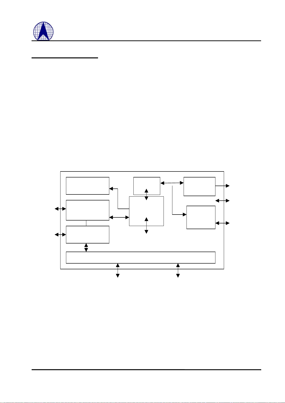
1.2 AX81190 Block Diagram
Two 8K*16 SRAM
MAC
Engine
S-EEPROM
LOADER IF
Registers
Buffer
Management
And FIFO
Power
Controller
Serial
I/F
Host Interface
EECS
EECLK
EEDI
EEDO
GPIO
PA_PE
. . .
BBP I/F
RF I/F
Ctrl BUS AD[31:0]
Page 7
ASIX ELECTRONICS CORPORATION
7
AX81190 PCI/CARDBUS/PCMCIA Bus WLAN MAC
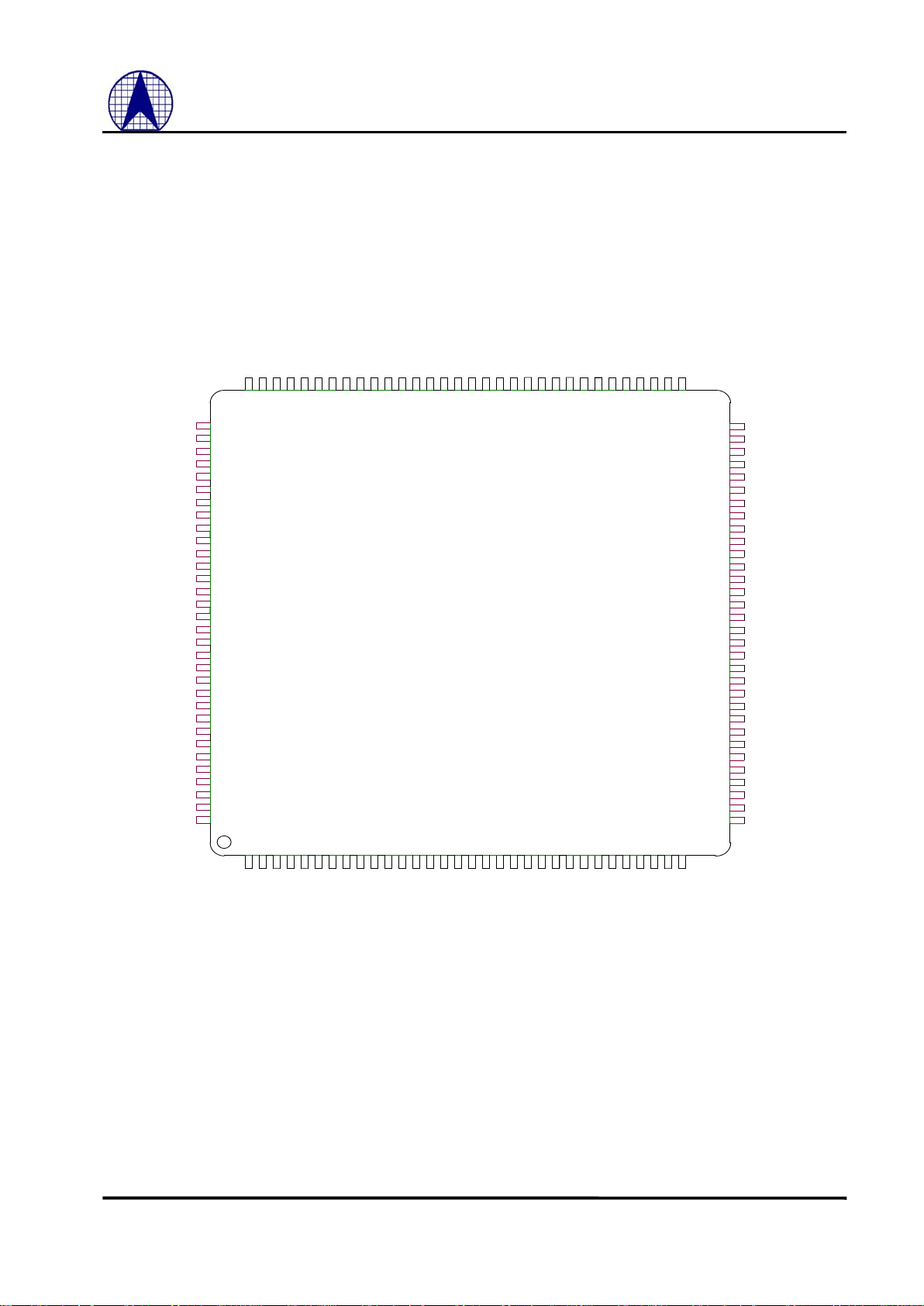
1.3 AX81190 Pin Connection Diagram
The AX81190 is housed in the 128-pin plastic quad flat pack
Fig - 1 AX81190 Pin Connection
Diagram
shows the AX81190 pin assignment.
1.3.1 AX88119 Pin Connection Diagram for PCMCIA Bus Mode
Fig - 1 AX81190 Pin Connection Diagram for PCMCIA Bus Mode
VSS1
IREQ#
10
VSS1
EEPM_DIS
TXD
A15
EECS
VSS1
GPIO2
GPIO0
SPI_DO
120
90
101
D8
81
51
62
86
A13
115
36
100
29
23
14
CCA
RF_PE
70
VDD2
GPIO3
LED1
40
D3
PE2
116
VSS1
BBPMODE0
D7
VSS2
D12
105
2
55
11
21
REG#
EECL
K
VDD2
SYNCLK
106
13
LED2
33
LE_IF#
99
CS#
117
D11
43
73
41
127
71
VDD1
SCLK
6
VDD2
D15
HRST
D1
AX81190
A3
78
92
MD_RDY
RSTPHY#
WE#
25
BBPMODE1 A1
VSS2
60
93
102
104
111
GPIO4
125
31
95
A14
VDD2
16
66
97
80
4
118
89
109
61
3
( PCMCIA )
TXCLK
67
NC
VSS1
82
49
12
VDD2
WAIT#
A5
34
D6
32
HBUSMODE
27
56
D0
108
OE#
MT0
A8
103
SYNDATA
CBSE
L
RX_PE
IOIS16#
91
69
PA_PE
85
A4
A0
VDD1
A2
44
57
48
VDD2
75
64
126
EED
O
MT1
113
79
RXCLK
84
VSS2
110
128
119
VDD1
RXD
NC
D14
VDD1
114
83
53
98
26
VDD1
VDD2
30
19
63
TX_RDY
EED
I
VDD1
SD
VSS2
65
VSS1
A11
VSS1
15
112
A6
VDD1
38
TX_PE
68
VSS1
77
D13
VSS2
D9
45
24
20
22
50
LE_RF#
47
NC
VDD1
8
124
39
88
121
59
D2
RW#
VSS2
VSS1
CAL_EN
VSS2
VSS1
37
TR_SW#
76
GPIO1
52
IORD#
94
42
IOWR#
96
7
VDD2
35
A7
107
87
D5
VDD1
46
A12
122
D4
CE1#
TR_SW
18
VSS2
NC
74
17
1
9
A9
D10
54
PE1
HCLK
GPIO5
72
A10
28
58
123
NC
5
Page 8

ASIX ELECTRONICS CORPORATION
8
AX81190 PCI/CARDBUS/PCMCIA Bus WLAN MAC
1.3.2 AX81190 Pin Connection Diagram for PCI/CardBus Mode
Fig - 2 AX81190 Pin Connection Diagram for PCI/CARDBUS
AD0
59
121
RF_PE
RSTPHY#
109
98
VDD1
PERR#
VSS1
74
99
50
EECL
K
26
AD12
9
PAR
93
GPIO3
VSS2
AD30
VDD1
AD5
86
AD7
AD2
STOP#
NC
120
AD14
VSS2
SD
AX81190
34
6
MT0
RX_PE
CS#
76
84
44
29
32
VSS1
RXCLK
15
AD9
111
78
21
83
123
68
AD20
AD19
70
RW#
91
VSS1
100
7
105
VSS2
128
PA_PE
107
IRDY#
EECS
BBPMODE0
75
46
16
19
CXBE0
#
39
TR_SW#
106
SYNDATA
CBSE
L
VDD1
AD15
8
127
31
AD21
TX_RDY
PE1
73
VSS1
67
63
GPIO5
VSS1
90
VDD1
3
22
47
18
AD11
AD28
125
13
AD17
79
81
( PCI )
115
AD26
HBUSMODE
57
2
17
AD29
VDD2
112
20
117
AD16
AD6
1
95
AD8
49
55
27
AD22
LE_IF#
116
102
60
HRST#
LE_RF#
EEPM_DIS
69
TRDY#
66
35
23
VDD2
AD1
10
MT1
77
VDD2
SYNCLK
124
VDD1
CCA
AD31
48
TXCLK
89
126
GPIO2
CXBE1
#
103
43
DEVSEL#
VSS1
VDD1
AD13
11
VSS1
28
37
53
62
VSS2
GPIO4
AD25
36
114
14
EED
I
AD18
52
87
CXBE2#
108
30
96
CAL_EN
113
TX_PE
FRAME#
VDD2
65
58
GPIO1
INTR#
VSS2
TXD
AD23
RXD
92
41
45
AD4
VSS2
122
SPI_DO
VSS2
82
85
119
38
HCLK
88
PE2
VDD2
42
64
110
CXBE3#
101
AD10
5
VDD1
LED2
94
AD24
80
12
VSS1
VSS1
VDD2
71
VSS2
25
EED
O
VSS1
VDD2
MD_RDY
TR_SW
72
54
24
IDSEL
SCLK
51
104
VDD2
BBPMODE1
VDD1
97
GPIO0
56
LED1
61
40
VDD1
AD27
33
4
AD3
118
Page 9

ASIX ELECTRONICS CORPORATION
9
AX81190 PCI/CARDBUS/PCMCIA Bus WLAN MAC
2.0 Signal Description
The following terms describe the AX81190 pin-out:
All pin names with the “#” suffix are asserted low.
The following abbreviations are used in following Tables.
I Input PU Internal Pull Up
O Output PD Internal Pull Down
I/O Input/Output P Power Pin
OD Open Drain
2.1 PCMCIA Bus Interface Signals Group
SIGNAL TYPE PIN NO. DESCRIPTION
HCLK I 28 Reference clock. 33Mhz or 44Mhz.
HRST I 26 Reset signal. Active high for PCMCIA.
A[15:0] I 61,62,33,34,
36,37,39,40,
44,45,46,47,
49,50,52,53
System Address : Signals A[15:0] are address bus input lines which
enable direct address of up to 64K memory and I/O spaces on card.
D[15:0] I/O 68,69,70,73,
74,76,77,78,
81,83,84,85,
86,88,89,91
System Data Bus : Signals D[15:0] constitute the bi-directional data
bus.
IREQ# O 24 Interrupt Request : IREQ# is asserted to indicate the host system that
the PC Card device requires host software service.
WAIT# O 64 Wait : This signal is set low to insert wait states during Remote DMA
transfer.
REG# I 42 Attribute Memory and I/O Space Select : When the REG# signal is
asserted, access is limited to Attribute Memory and to the I/O space.
IORD# I 55 I/O Read : The host asserts IORD# to read data from AX81190 I/O
space.
IOWR# I 41 I/O Write : The host asserts IOWR# to write data into AX81190 I/O
space.
OE# I 32 Output Enable : The OE# line is used to gate Memory Read data from
memory on PC Card
WE# I 30 Write Enable : The WE# signal is used for strobing Memory Write
data into the memory on PC Card.
IOIS16# O 56 I/O is 16 Bit Port : The IOIS16# is asserted when the address at the
socket corresponds to an I/O address to which the card responds, and
the I/O port addressed is capable of 16-bit access.
CE1# I 80 Card Enable : The CE1# enables even numbered address bytes.
PCMCIA bus interface signals group
Page 10

ASIX ELECTRONICS CORPORATION
10
AX81190 PCI/CARDBUS/PCMCIA Bus WLAN MAC
2.2 PCI/CARDBUS Bus Interface Signals Group
SIGNAL TYPE PIN NO. DESCRIPTION
HCLK I 28 The clock provides the timing for the AX81190 related PCI bus
transactions. All the bus signals are sampled on the rising edge of
HCLK. The max frequency is 33MHz.
HRST# I 26 Resets the AX81190 to its initial state. This signal must be asserted
for at least 10 active PCI clock cycles. When is the reset state, all PCI
output pins are put into tri-state and all PCI o/d signals are floated.
FRAME# I/O 56 The FRAME# Signal is driven by the master to indicate the beginning
and duration of an access. FRAME# Asserts to indicate the beginning
of a bus transaction. While FRAME# is asserted, data transfers
continue. When FRAME# deasserts the next data phase is the final
data phase transaction.
IRDY# I/O 58
Initiator ready Indicates the bus master ability to complete the
current data phase of the transaction.
A data phase is completed on any rising edge of the clock When both
IRDY# and target ready TRDY# are asserted. Wait cycles are
inserted until both IRDY# and TRDY# are asserted together.
TRDY# I/O 59 Target ready indicates the target ability to complete the current data
p
hase of the transaction. A data phase is completed on any clock when
b
oth TRDY# and IRDY# are asserted. Wait cycles are inserted until
both IRDY# and TRDY# are asserted together.
DEVSEL# I/O 61 Device select Is asserted by the AX81190 of the current bus access hit
to AX81190
STOP# I/O 62 Stop indicator indicates that the current target is requesting the bus
master to stop the current transaction.
PAR I/O 65 Parity is an even parity bit for the AD[31:0] AD and CXBE[3:0]#.
During address and data phases, parity is calculated on all the
AD[31:0] AND CXBE[3:0]# lines whether or not any of these lines
carry meaningful information.
IDSEL I 42 Initialization devise select asserts To indicate that the host is issuing a
configuration cycle to the AX81190. For cardbus application, this pin
always is pulled high with VDD1.
AD[31:0] I/O 30,32,33,34,
36,37,39,40,
44,45,46,47,
49,50,52,53,
68,69,70,73,
74,76,77,78,
81,83,84,85,
86,88,89,91
Address and data bits are multiplexed on the same pins. During the
address phase, the AD[31:0] contain a physical address (32 bits).
During, data phases, AD[31:0] contain 32 bits of data.
CXBE[3:0]# I/O 41,55,66,80 BUS COMMAND and BYTE ENABLE Are multiplexed on the same
PCI pins. During the address phase of the transaction, CXBE[3:0]#
Provide the BUS COMMAND. During the data phase, CXBE[3:0]#
Provide the BYTE ENABLE. The BYTE ENABLE determines
which byte lines carry valid data., CXBE0# Applies to byte 0, and
CXBE3# Applies to byte 3.
PERR# I/O 63 Parity error asserts when a data parity error is detected. when a parity
error is detected, the AX81190 asserts PERR#. This pin must be
pulled up with VDD2 by an external resistor.
Page 11

ASIX ELECTRONICS CORPORATION
11
AX81190 PCI/CARDBUS/PCMCIA Bus WLAN MAC
INTR# O/D 24 Interrupt request asserts When one of the appropriate bits of Interrupt
Status Register sets and causes an interrupt, provided that the
corresponding mask bit in Interrupt Mask Register is not asserted.
Interrupt request deasserts by writing an “1” into the appropriate
Interrupt Status Register bit.
This pin must be pulled up with VDD2 by an external resistor.
PCI/CARDBUS bus interface signals group
2.3 EEPROM Signals Group
SIGNAL TYPE PIN NO. DESCRIPTION
EECS O 96 EEPROM Chip Select : EEPROM chip select signal.
EECLK O 94 EEPROM Clock : Signal connected to EEPROM clock pin.
EEDI O 93 EEPROM Data In : Signal connected to EEPROM data input pin.
EEDO I/PD 92 EEPROM Data Out : Signal connected to EEPROM data output pin.
EEPROM bus interface signals group
2.4 Serial Port Interface Signals Group
SIGNAL TYPE PIN NO. DESCRIPTION
SCLK O 9 SCLK is the clock for SD serial bus. The data on SD is latched in
rising edge.
SD I/O/PD 10 SD is serial bi-directional data bus, which is used to transfer address
and data to/from BBP internal register for Intersil type BBP.
This signal is input only for RFMD type BBP.
SPI_DO O 12 SPI_DO is serial data output only bus, which is used to transfer
address and data to RFMD type BBP.
RW# O 7 To control the direction when MAC reads or writes data on SD bus. A
high level indicates a read cycle and low level indicates a write cycle.
CS# O 8 MAC selects BBP to be as target.
Serial port interface signals group
2.5 Baseband Processer Controller interface signals group
SIGNAL TYPE PIN NO. DESCRIPTION
TXD O 1 MAC transmits data to BBP. The data is valid in rising edge of
TXCLK.
TXCLK I 2 The clock from BBP is to be valid TXD.
TX_RDY I 111 BBP indicates the valid data phase.
TX_PE O 117 To control the transmitted phase.
CCA I 113 MAC will monitor this signal to determine whether it can transmit
data or not.
RXD I 4 RXD is an input from BBP. The data is sent serially with LSB first
and the data is frame aligned with RX_RDY.
Page 12

ASIX ELECTRONICS CORPORATION
12
AX81190 PCI/CARDBUS/PCMCIA Bus WLAN MAC
RXCLK I 5 This is the bit clock input from BBP. This clock is used to transfer
header information and payload data through the RXD serial bus.
RXCLK becomes active after SFD has been detected. Data (RXD)
should be samples on rising edge.
MD_RDY I 114 BBP indicates header data and data packet are ready to be transferred.
RX_PE O 115 MAC enables BBP to qualify receive stage.
Baseband Processer interface signals group
2.6 Power Control Interface Signals Group
SIGNAL TYPE PIN NO. DESCRIPTION
CAL_EN O 125 Calibration mode enable.
TR_SW#
O 120 Transmit & Receive Switch Control. Active low.
TR_SW
O 119 Transmit & Receive Switch Control. Active High.
PA_PE O 122 Power Amplifier control pin,. Active high.
RF_PE O 121 Power enable pin to RF and IF components.
PE1 O 13 Power enable1 for I/Q Modulation/Demodulation
PE2 O 15 Power enable2 for I/Q Modulation /Demodulation
Power Control interface signals group
2.7 Synthesizer control signal Interface pins group
SIGNAL TYPE PIN NO. DESCRIPTION
SYNDATA O 128 Serial data for front-end chip synthesizer.
SYNCLK O 127 Serial clock for front-end chip synthesizer.
LE_IF# O 123 Load (latch) Enable to IF synthesizer. MAC selects IF as target for
serial access.
LE_RF# O 124 Load (latch) Enable RF synthesizer. MAC selects RF as target for
serial access
Channel Activity Status Interface pins group
2.8 Miscellaneous pins group
SIGNAL TYPE PIN NO. DESCRIPTION
RSTPHY# O 14 MAC will reset BBP when it monitors the system-reset occurred. Due
to power management issue, MAC will drive BBP into stand-
b
y mode
by RSTPHY# signal driven low for Intersil-like BBP or high for
RFMD-like BBP.
HbusMode I/PU 106 Pull high with VDD2 for PCI/CARDBUS operation
Pull low with VSS2 for PCMCIA operation.
CBSEL I/PD 71 Pull high for CRADBUS operation. In Cardbus mode, Both
HbusMode and CBSEL are also pulled high.
BBPMODE[1:0] I/PU 108,109 BBP interface selection.
2’b00: For Intersil-like interface.
2’b01: For RFMD-like interface.
2’b10: Reserved
2’b11: For RaLink BBP.
Page 13

ASIX ELECTRONICS CORPORATION
13
AX81190 PCI/CARDBUS/PCMCIA Bus WLAN MAC
LED1 O 17 Indicates in transmitted state.
LED2 O 19 Indicates in received state.
EEPM_DIS I/PD 97 Reserved, pull down with VSS2 for normal operation.
MT[1:0] I/PD 99,100 Memory Test, pull down with VSS2 (2’b00) for normal operation.
GPIO[5:0] I/O/PD 21,22,102,
103,104,105
General pins are cotrolled by software.
VDD1 P 11,16,25,38,
54,72,79,110,
126
Power Supply: +2.5V DC.
VDD2 P 20,31,48,60,
82,87,98,116
Power Supply: +3.3V DC.
VSS1 P 3,18,27,35,51
,57,67,90,107
,112
Ground pin for +2.5V.
VSS2 P 6,23,29,43,75
,95,101,118
Ground pin for +3.3V.
Miscellaneous pins group
Page 14

ASIX ELECTRONICS CORPORATION
14
AX81190 PCI/CARDBUS/PCMCIA Bus WLAN MAC
3.0 Registers Operation
R Read Only RC Read to Clear
W Write Only WC Write “one” to Clear
WO Write “one” Only
3.1 PCI Configuration Register
3.1.1 Device vendor register -- offset 00h
Field R/W Default Description
31:16 R 1190h Indicate the Device ID in PCI system.
15:0 R 125Bh ASIX Vendor ID.
3.1.2 Command register – offset 04h
Field R/W Default Description
15-10 R 6’b000000 Reserved.
9 R 0 Fast back-to-back transactions. Always 0, this function is not
supported.
8 R 0 SERR_ enable function. Always 0, this function is not supported.
7 R 0 Address/data step function. Always 0, this function is not supported.
6 R/W 0 Parity error response function. If set high, interface will response
parity error message via PERR_. If this bit is 0, interface will ignore
parity error.
Default:0
5 R 0 VGA snooping. Always 0, not supported.
4 R 0 Memory write and invalid command. Always 0, interface will not
generate this command.
3 R 0 Special cycle response. Always 0, interface ignores all special cycle.
2 R 0 Bus master control. Interface does not support master function.
1 R/W 0 Memory space response enable.
0 R/W 0 I/O space control. If it is set to ‘0’, interface does not response io
access, otherwise interface will response io access.
3.1.3 Status register – offset 06h
Field R/W Default Description
15 R/WC 0 PERR_ detected. Set to ‘1 whenever parity error is detected, Write ‘1’
to clear.
14 R 0 SERR_ detected.
13 R 0 Receive master abort.
12 R 0 Receive target abort.
11 R 0 Target abort.
10:9 R 0 Timing.
8 R 0 PERR_ reported.
7 R 0 Fast back-to-back capability, Always 0.
6 R 0 User define features. Always 0.
5 R 0 66MHz capability. Always 0, interface is not supported 66 MHz.
4 R 0 Capability bit. Always 0.
3:0 R 4’b0000 Reserved. Always 4’b0000
3.1.4 Revision ID register – offset 08h
Page 15

ASIX ELECTRONICS CORPORATION
15
AX81190 PCI/CARDBUS/PCMCIA Bus WLAN MAC
Bit R/W Default Description
7:0 R 00h Current revision, the value is 01h now.
3.1.5 Class code register – offset 09h
Bit R/W Default Description
23:0 R 020000h Ethernet Network controller.
3.1.6 Base IO address register – offset 10h
Bit R/W Default Description
31:16 R 0 Reserved
15:7 R/W 0 To be mapped in 64K in space
6:1 R 0 Reserved.
0 R 1 IO space indicator.
3.1.7 Base Memory address register – offset 14h
Bit R/W Default Description
31:8 R/W 0 To 4G memory space.
7:0 R 0 Reserved.
3.1.8 CIS pointer – offset 28h
3.1.9 Subsystem ID – 2Ch
Bit R/W Default Description
31:16 R/W 1190h Download from EEPROM when power on.
15:0 R/W 125Bh Download from EEPROM when power on.
3.1.10 Interrupt register – 3Ch
Bit R/W Default Description
15:8 R 01h Interrupt pin assigned. The value is always 01h.
7:0 R/W FFh Interrupt line routing information. Default value is FFh.
Page 16

ASIX ELECTRONICS CORPORATION
16
AX81190 PCI/CARDBUS/PCMCIA Bus WLAN MAC
3.2 PCMCIA Configuration Register
In PCMCIA application, there are four registers, 800h, 802h, 804, and 806h located in attribute memory.
3.2.1 COR register – 0800h
Field R/W Default Description
7 R/W 0 Soft reset enable. Set to ‘1’ to reset MAC core. MAC will reset this bit if it finished
reset operation. This function is replaced with base_e register.
6 R 0 Reserved
5:0 R/W 0
Configure index, Set to non-zero’s bit to enable IO transfer.
3.2.2 CCR register – 0802h
Field R/W Default Description
7:6 R 0 Reseerved
5 R 0 IOIS8 indicator. MAC always responses 16-bit access except the memory access.
4: R 0 Reserved.
3.2.3 IO base (LSB) – 0804h
Field R/W Default Description
7:0 R/w 0 For io base address pointer (LSB)
3.2.4 IO base (MSB) – 0806h
Field R/W Default Description
7:0 R/w 0 For io base address pointer (MSB)
Page 17

ASIX ELECTRONICS CORPORATION
17
AX81190 PCI/CARDBUS/PCMCIA Bus WLAN MAC
3.3 IO port
3.3.1 CSR index port base
Field R/W Default Description
15-8 R 0 Reserved
7-0 R/W 0 Selects the CSR location of MAC to be accessed.
3.3.2 CSR data port base + 2
Field R/W Default Description
15-0 R/W 0 16-bit data port for MAC control and status register accesses.
3.3.3 Tx Data access control port base + 4
Field R/W Default Description
15 R/W 0 Enable for data burst. Driver can set this bit to ‘1’. Hardware will automatically
increase address when driver accesses Tx data buffer port.
14:12 R/W 0 3’b111: for beacon information to be transmitted
3’b110: for probe response frame to be transmitted
Others : for general data to be transmitted. AX81190 support 6 pages for general data
using.
11:0 R/W 0 Address for internal TX memory access. (byte access)
3.3.4 Tx data buffer port base + 6
Field R/W Default Description
15-0 R/W 0 16-bit port for MAC internal tx data buffer access
3.3.5 Rx Data access control port base + 8
Field R/W Default Description
15 R/W 0 Burst enable for access RX buffer.
14:11 R/W 0 RX buffer page pointer. There are 10 pages available and valid range is from 0 to 9.
10:0 R/W 0 Address for internal RX buffer access. (word access)
3.3.6 Rx data buffer port base + ah
Field R/W Default Description
15-0 R/W 0 16-bit port for MAC internal rx data buffer access
3.3.7 Soft reset port base + eh
Field R/W Default Description
15:2 R/W 0 Reserved
1 R/W 0 If set to ‘1’, MAC will reset BBP. This bit will be reset when it was finished
operation.
0 R/W 0 If set to ‘1’, MAC will reset internal core. When MAC finished reset itself, it will
reset this bit to ‘0’. The reset only affected buffer management and protocol control
unit.
3.3.8 Interrupt status port base + 10h
Field R/W Default Description
15:11 R 0 Reserved
10 R/WC 0 TX packet length error.
9 R 0 Reserved
8 R/WC 0 TBTT time-out indication.
Page 18

ASIX ELECTRONICS CORPORATION
18
AX81190 PCI/CARDBUS/PCMCIA Bus WLAN MAC
7 R/WC 0 RX data indicator. When MAC has received data from another station and these are
been stored in internal buffer. This bit will be set to 1 while data is completed in
buffer. MAC will interrupt host to check the status.
6 R/WC 0 TX data complete indicator. When MAC has successfully sended out data and it
obtains a ACK returned or no needs ACK, this bit will be set to high. Driver can
approach this bit to determine the status.
5 R/WC 0 Tx fail. When MAC issues a transmit frame and finds no response corresponding
frame.
4 R/WC 0 Tx beacon finish.
3 R/WC 0 Protocol change event. This bit indicates there is a protocol changed.
2 R/WC 0 ATIM window end.
1 R/WC 0 Soft reset complete.
0 R/WC 0 Rx buffer full indication.
3.3.9 Interrupt mask port base + 12h
Field R/W Default Description
15:11 R 0 Reserved
10 R/W 0 Set ‘1’ to enable corresponding event that generates interrupt.
9 R 0 Reserved
8 R/W 0 Set ‘1’ to enable corresponding event that generates interrupt.
7 R/W 0 Set ‘1’ to enable corresponding event that generates interrupt.
6 R/W 0 Set ‘1’ to enable corresponding event that generates interrupt.
5 R/W 0 Set ‘1’ to enable corresponding event that generates interrupt.
4 R/W 0 Set ‘1’ to enable corresponding event that generates interrupt.
3 R/W 0 Set ‘1’ to enable corresponding event that generates interrupt.
2 R/W 0 Set ‘1’to enable corresponding event that generates interrupt.
1 R/W 0 Set ‘1’to enable corresponding event that generates interrupt.
0 R/W 0 Set ‘1’to enable corresponding event that generates interrupt.
3.3.10 Rx page status port base + 14h
Field R/W Default Description
15:10 R 0 Reserved
9 R/WC 0 This bit indicates that there is a packet stored in page9 of rx buffer.
8 R/WC 0 This bit indicates that there is a packet stored in page8 of rx buffer.
7 R/WC 0 This bit indicates that there is a packet stored in page7 of rx buffer.
6 R/WC 0 This bit indicates that there is a packet stored in page6 of rx buffer.
5 R/WC 0 This bit indicates that there is a packet stored in page5 of rx buffer.
4 R/WC 0 This bit indicates that there is a packet stored in page4 of rx buffer.
3 R/WC 0 This bit indicates that there is a packet stored in page3 of rx buffer.
2 R/WC 0 This bit indicates that there is a packet stored in page2 of rx buffer.
1 R/WC 0 This bit indicates that there is a packet stored in page1 of rx buffer.
0 R/WC 0 This bit indicates that there is a packet stored in page0 of rx buffer.
3.3.11 Tx page status port1 base + 16h
Field R/W Default Description
15 R/WO 0 Beacon packet indicator. If set to ‘1’ means data occupied the beacon buffer. Driver
set this bit to ‘1’ and AX81190 will reset it if it transmits out the beacon packet.
14:6 R 0 Reserved.
5 R/WO 0 If set to ‘1’ means data occupied the page5 of tx buffer. Driver set this bit to ‘1’ and
AX81190 will reset it if it transmits out the packet.
4 R/WO 0 If set to ‘1’ means data occupied the page4 of tx buffer. Driver set this bit to ‘1’ and
AX81190 will reset it if it transmits out the packet.
3 R/WO 0 If set to ‘1’ means data occupied the page3 of tx buffer. Driver set this bit to ‘1’ and
AX81190 will reset it if it transmits out the packet.
Page 19

ASIX ELECTRONICS CORPORATION
19
AX81190 PCI/CARDBUS/PCMCIA Bus WLAN MAC
2 R/WO 0 If set to ‘1’ means data occupied the page2 of tx buffer. Driver set this bit to ‘1’ and
AX81190 will reset it if it transmits out the packet.
1 R/WO 0 If set to ‘1’ means data occupied the page1 of tx buffer. Driver set this bit to ‘1’ and
AX81190 will reset it if it transmits out the packet.
0 R/WO 0 If set to ‘1’ means data occupied the page0 of tx buffer. Driver set this bit to ‘1’ and
AX81190 will reset it if it transmits out the packet.
3.3.12 Tx page status port2 base + 18h
Field R/W Default Description
15:6 R 0 Reserved
5 RC 0 If set to ‘1’ means page5 fail in transmittance.
4 RC 0 If set to ‘1’ means page4 fail in transmittance.
3 RC 0 If set to ‘1’ means page3 fail in transmittance.
2 RC 0 If set to ‘1’ means page2 fail in transmittance.
1 RC 0 If set to ‘1’ means page1 fail in transmittance.
0 RC 0 If set to ‘1’ means page0 fail in transmittance.
3.3.13 BBP_index port base + 1ah
Field R/W Default Description
15 R/W 0 Write BBP register enable bit. BBP controlling flag (open bit). If set to 1, any access
to BBP_data port register will generate serial write cycle between BBP and MAC.
When MAC completes the access, it will reset this bit to 0.
14 R/W 0 Read BBP register enable bit. If this bit is set to 1, MAC will generate serial read
cycle to BBP. Default is 0. When MAC completes the access, it will reset this bit to 0.
13:8 R/W 0 Reserved
7:0 R/W 0 BBP internal register’s index.
3.3.14 BBP_data out port base + 1ch
Field R/W Default Description
15:8 R 0 Reserved
7:0 R/W 0 Contained the data will be out to BBP.
3.3.15 BBP_data in port base + 1eh
Field R/W Default Description
15:8 R 0 Reserved
7:0 R/W 0 Store the data read from BBP internal registers.
3.3.16 Synthesizer control port base + 20h
Field R/W Default Description
15:9 R 0 Reserved
8 R/W 0 Start program PLL phase
7 R/W 0 IF PLL latch enable. Self-reset if it finished programming IF chip.
6 R/W 0 RF PLL latch enable. Self-reset if it finished. Programming RF chip.
5:0 R/W 14h Contain bit-length to program PLL of synthesizer. Max value is 32.
3.3.17 Synthesizer data port0 base + 22h
Field R/W Default Description
15:0 R/W 0 The register contains lower 16 bits data that want to program to PLL of synthesizer.
3.3.18 Synthesizer data port1 base + 24h
Field R/W Default Description
15:0 R/W 0 The register contains higher 4 to 16 bits data that want to program to PLL of
Page 20

ASIX ELECTRONICS CORPORATION
20
AX81190 PCI/CARDBUS/PCMCIA Bus WLAN MAC
synthesizer.
3.3.19 EE_data port base + 26h
Field R/W Default Description
15:0 R/W 0 16 bit data port for serial EEPROM access.
3.3.20 EE_cmd/addr port base + 28h
Field R/W Default Description
15:13 R/W 0 Command Type.
3’b110 : read
3’b111 : Erase
3’b101 : write
3’b100: erase/write enable
12 R/W 0 Set to ‘1’ to enable write EEPROM, it will be reset if MAC finished the write
operation.
11 R/W 0 Set to ‘1’ to enable read EEPROM, it will be reset if MAC finished the read
operation. Driver can read base_26 port to get the data.
10 R/W 0 Set to ‘1’ to indicate MAC to verify the write operation.
9:8 R 0 Reserved
7:0
R/W 0
Address for serial EEPROM access. (only support 16 bit data access
)
93c56 : use A7 ~ A0, but A7 always is’0’
3.3.21 EE_status_type port base + 2ah
Field Type Default Description
15:9 R 0 Reserved
8 R 0 If set to ‘1’ means MAC is currently loading data from EEPROM.
5:4 R 2’b01 Serial EEPROM configuration indicator.
2’b01 : 93C56 supported.
3 R 0 Reserved.
2:0 R 3’b001 Serial EEPROM clock rate indicator.
3’b001 : 1MHz..
Page 21

ASIX ELECTRONICS CORPORATION
21
AX81190 PCI/CARDBUS/PCMCIA Bus WLAN MAC
3.4 MAC Configuration Status Registers
3.4.1 CSR1 – MAC Physical address0 (PADR[15:0])
Field R/W Default Description
15:0 R 0 Physical address register. When power-on, MAC loads data from external EEPROM
and update this register once.
3.4.2 CSR2 – MAC Physical address1 (PADR[31:16])
Field R/W Default Description
15:0 R 0 Physical address register. When power-on, MAC loads data from external EEPROM
and update this register once.
3.4.3 CSR3 – MAC Physical address2 (PADR[47:32])
Field R/W Default Description
15:0 R 0 Physical address register. When power-on, MAC loads data from external EEPROM
and update this register once.
3.4.4 CSR4 – BSSID Matching Register0, BSSID[15:0]
Field R/W Default Description
15:0 R/W 0 This 16-LSB of the 48-bit Address3 matching pattern.
3.4.5 CSR5 – BSSID Matching Register1, BSSID[31:16]
Field R/W Default Description
15:0 R/W 0 This 16-CSB of the 48-bit Address3 matching pattern.
3.4.6 CSR6 – BSSID Matching Register2, BSSID[47:32]
Field R/W Default Description
15:0 R/W 0 This 16-MSB of the 48-bit Address3 matching pattern.
3.4.7 CSR7 ~ CSR9 are reserved.
3.4.10 CSR10 – Multicast filter pattern1
Field R/W Default Description
15:0 R/W 0 This field defines the filtering pattern for multicast frame
Note: When m_csr29 bit6 is enabled, this register will be referred.
3.4.11 CSR11 – Multicast filter pattern2
Field R/W Default Description
15:0 R/W 0 This field defines the filtering pattern for multicast frame
Note: When m_csr29 bit6 is enabled, this register will be referred.
3.4.12 CSR12 – Multicast filter pattern3
Field R/W Default Description
15:0 R/W 0 This field defines the filtering pattern for multicast frame
Note: When m_csr29 bit6 is enabled, this register will be referred.
3.4.13 CSR13 – Multicast filter pattern4
Field R/W Default Description
15:0 R/W 0 This field defines the filtering pattern for multicast frame
Page 22

ASIX ELECTRONICS CORPORATION
22
AX81190 PCI/CARDBUS/PCMCIA Bus WLAN MAC
Note: When m_csr29 bit6 is enabled, this register will be referred.
Note: Multicast filter matrix
CSR10[7:0] 7 6 5 4 3 2 1 0
CSR10[15:8] 15 14 13 12 11 10 9 8
CSR11[7:0] 23 22 21 20 19 18 17 16
CSR11[15:8] 31 30 29 28 27 26 25 24
CSR12[7:0] 39 38 37 36 35 34 33 32
CSR12[15:8] 47 46 45 44 43 42 41 40
CSR13[7:0] 55 54 53 52 51 50 49 48
CSR13[15:8] 63 62 61 60 59 58 57 56
3.4.12 CSR14 ~ CSR15 are reserved.
3.4.16 CSR16 – clock pattern
Field R/W Default Description
15:12 R 0 Reserved.
11:8 R/W fh RTS-CTS max duration
7:0 R/W 10h Set to 10h if use 33Mhz host clock.
Set to 16h if use 44Mhz host clock.
3.4.17 CSR17 – Wait md_rdy duration
Field R/W Default Description
7:0 R/W 14h The duration mac waited for the md_rdy, if there is PLCP field is found.
.
3.4.18 CSR18 – Short Interframe space timing register ,SIFS
Field R/W Default Description
15:0 R/W 0Ah This field defines the timing slice of short interfame space timing. The timing unit is
1us.
3.4.19 CSR19 – Distributed Interframe space timing register, DIFS/PIFS
Field R/W Default Description
15:0 R/W 20h This field defines the timing slice of DIFS space timing. The timing unit is 1us.
3.4.20 CSR20 ~ CSR 21 – Reserved.
3.4.22 CSR22 – SlotTime Register (SLOT)
Field R/W Default Description
15:0 R/W 14h The SLOT time register is written to by some proper values by the driver. It determines
the unit of the backoff time. The unit of the register value is in μs.
3.4.23 CSR23 – Backoff timing
Field R/W Default Description
15:0 R 0 To show the backoff timing of MAC.
3.4.24 CSR24 – RF3000 modulation duration (Testing)
Field R/W Default Description
15:0 R/W 4000h Available when RF3000 BBP is used.
3.4.25 CSR25 – Power Testing and misc
Field R/W Default Description
Page 23

ASIX ELECTRONICS CORPORATION
23
AX81190 PCI/CARDBUS/PCMCIA Bus WLAN MAC
15 R/W 0 1: Tx power enable.
0: None
14 R/W 0 Tx power pattern.
13 R/W 0 1: Tx power toggle enable.
0: None
12 R/W 0 Reserved
11 R/W 0 1: enable software control
0: None
10 R/W 0 Reserved
9 R/W 0 Reserved
8 R/W 0 Software control SynData
7 R/W 0 Software control SynCLK
6 R/W 0 Software control LE_RF#
5 R/W 0 Software control RF_PE
4 R/W 0 Software control PE2.
3 R/W 0 Software control PE1
2 R/W 0 Software control PA_PE
1 R/W 0 Software control RX_PE
0 R/W 0 Software control TX_PE
3.4.26 CSR26 – TXVGC adjust register (support RF3000 only)
Field R/W Default Description
7 R/W 0 0: long preamble
1: short preamble
6:1 R/W 25h Gain setting for transmission.
0 R/W 0 Scrambler indication.
0 : enable
1: Disable
3.4.27 CSR27 – Tx Beacon/probe response enable register
Field R/W Default Description
7:2 R 0 Reserved.
1 R/W 0 1: Enable MAC to grab data from beacon buffer and transmit the data.
The data is especially for probe response frame used and max length can not exceed
512 byte.
0 R/W 0 1: Enable MAC to grab data from beacon buffer and transmit the data. MAC will reset
this bit if it finished the transmittance. The max length can not exceed 512 byte.
3.4.28 CSR28 – TBTT Compensation Register
Field R/W Default Description
15:10 R 0 Reserved
9:0 R/W 0
This 10-
b
it register, which is used to compensate the calculation delay of TBTT
generation circuit. It can also be used to compensate the driver’s processing delay to
generate a beacon frame.
The unit of the value is in μs.
3.4.29 CSR29 – Rx filtering Register
Field RW Default Description
15:11 R/W 0 Reserved
10 R/W 0 Multicast algorithm selection.
0: select XOR
1: select CRC32.
9 R/W 0 1: Enable Rx length filtering.
8 R/W 0 1: Force rx enable. (Always enable RX_PE to be high)
Page 24

ASIX ELECTRONICS CORPORATION
24
AX81190 PCI/CARDBUS/PCMCIA Bus WLAN MAC
7 R/W 0 Enable broadcast reception. If set to 0, all broadcast frames will be dropped.
6 R/W 0 Enable multicast filtering. If set to 1, only the multicasts whose Address1 field
matches the matching criteria will be passed to the driver. The default is 0.
5 R/W 0 Enable multicast reception. If set to 1, multicast frames will be received, and no
logical address matching will be performed.
4 R/W 0 Reserved
3 R/W 0 CRC32 check enabled. If set to 1, the CRC32 fields with will be verified.
2 R/W 0 Control frame enable. If set to 1, all control frames received will be passed to the
driver.
1 R/W 0 Promiscuous mode enabled. If set to 1, all data/mgmt frames will be passed to the
driver.
0 R/W 0 RX enable. This bit defines whenever MAC can receive data. Driver must set this bit
to ‘1’ to enable receive mode.
3.4.30 CSR30 – TX Power Ramp-up Control Register1
Field RW Default Description
15:0 R/W 0Ah This field defines the TX_PE lagged time when RX_PE was driven low.
3.4.31 CSR31 – TX Power Ramp-up Control Register2
Bit RW Default Description
15:0 R/W 14h This field defines pe2 lagged time when rx_pe was driven low.
3.4.32 CSR32 – TX Power Ramp Control Register3
Bit R/W Default Description
15:0 R/W 1bh This field defines the pa_pe lagged time when rx_pe was driven low.
3.4.33 CSR33 – TX Power Ramp Control Register4
Bit R/W Default Description
15:0 R/W 46h This field defines the tr_sw lagged time when rx_pe was driven low.
3.4.34 CSR34 – TX Power Ramp Control Register5
Bit R/W Default Description
15:0 R/W bdh This field defines the duration before RX_PE asserted. The start point is
based on last bit to be transmitted.
3.4.35 CSR35 – BeaconPeriod (BP)
Field R/W Default Description
15:0 R/W 0200h This 16 bit register, which is used to uniquely define the Target Beacon Transmission
Time (TBTT). The unit of the value is Kus.
3.4.36 CSR36 – Tx Retry counter
Field RW Default Description
7:0 R/W 10h Tx Retry counter. This register defines the retry number. MAC will assert a packet, if
there is no relative frame returned.
3.4.37 CSR37 – MAC feature register
Field R/W Default Description
15 R/W 0 The duration field of RTS frame is from data or information header.
1: From data.
0: From information header.
14 R/W 0 1: Enable NAV mechanism for channel status.
Page 25

ASIX ELECTRONICS CORPORATION
25
AX81190 PCI/CARDBUS/PCMCIA Bus WLAN MAC
13 R/W 1 1: Disable to set Intersil 3861 CR31 register
0: MAC will set the Intersil 3861 before transmittance.
12 R/W 0 PE2 polarity.
11 R/W 0 1 : to reset TSF timer, MAC will clear this bit when the reset is finished.
10 R/W 0 1:Tx stop normal page. Driver set this bit to stop the transmittance.
9 R/W 0 1:Tx stop urgent page. Driver set this bit to stop the transmittance.
8 R/W 1 Inbuf overflow protect.
1: Protect when inbuf is full. Data will not be written to inbuf.
0: No protect. Data will be written to inbuf, regardless of inbuf whether it is full or
not.
7 R/W 0 Backoff procedure disable. When set to 1, backoff procedure will ignore. MAC will
be prepared to request medium immediately whenever it has data to be sent.
6 R/W 0 CCA Enable.
5 R/W 0 CCA polarity for channel available. (RFMD)
4 R/W 0 To indicate MAC employs 3-wire or 4-wire approach to program BBP.
0: 3-wire, Use CS#, SCLK and SD signals.
1: 4-wire, Use CS#, SCLK, SD and RW# signals.
3 R/W 0 1: Latch SQ enable.
0: Nothing
2 R/W 0 1: Latch RSSI enable.
0: Nothing
1 R/W 1 PE1 polarity.
0: Active low
1: Active high.
0 R/W 0 RF_PE (Radio-PD) polarity.
0: Active low
1: Active high
3.4.38 CSR38 is Reserved
3.4.39 CSR39 – Transmit page control register
Field R/W Default Description
7 R/W 0 If this bit is set, it claims this transaction has the priority; otherwise, it is a normal
transmittance.
6:3 R/W 0 Reserved
2:0 R/W 0 Driver set this field to claim which the page data will be transmitted.
2’b000: page0 to be transmitted.
2’b001: page1 to be transmitted.
2’b010: page2 to be transmitted.
2’b011: page3 to be transmitted.
2’b100: page4 to be transmitted.
2’b101: page5 to be transmitted.
3.4.40 CSR40 – TX Rate control register.
Field R/W Default Description
15 R 0 Reserved
14:12 R/W 3’b000 RTS speed control
3’b000: auto
3’b001: 1M
3’b010: 2M
3’b011: 5.5M
3’b100: 11M
Others: reserved
11 R 0 Reserved
10:8 R/W 3’b000 ACK/CTS speed control
Page 26

ASIX ELECTRONICS CORPORATION
26
AX81190 PCI/CARDBUS/PCMCIA Bus WLAN MAC
3’b000: auto
3’b001: 1M
3’b010: 2M
3’b011: 5.5M
3’b100: 11M
Others: reserved
7:5 R 0 Reversed.
4 0 Tx/Rx filter CMF weight.
0 = U.S.
1=Japan.
3 R/W 0 Select preamble mode
0= Normal, long preamble
1= short preamble and header mode.
2:0 R 0 Reserved
Bit7 ~ bit0 is only for Intersil 3861/3863.
3.4.41 CSR41 – response time-out register
Field R/W Default Description
15:0 R/W 0145h MAC will count the time when it desires CTS/ACK returned. The time unit is us.
3.4.42 CSR42 – RSSI-SQ location register
Field R/W Default Description
15:8 R/W 72h SQ location in BBP
7:0 R/W 7Ch RSSI location in BBP.
For 3861 set to 727Ch
For R3000 set to xx03h.
3.4.43 CSR43 – TSF compensate register
Field R/W Default Description
15 R/W 0 This bit defines how many us need to compensate the TSF timer when MAC
transmitted beacon frame.
0: MAC will add bit[14:0] value to TSF timer.
1: MAC will deduct bit[14:0] value from TSF timer and inserted the final value to
frame body of beacon.
14:0 R/W 0 Compensate value for TSF. This unit is us.
3.4.44 CSR44 – Calibration adjust register
Field R/W Default Description
15 R/W 0 Calibration enable. If set, MAC will drive cal_en pin. Driver set this bit to 1 to enable
calibration mode. If MAC finished calibration, it will reset it to 0.
14 R/W 0 Set to ‘1’ to enable cal_en until it’s cleared.
13:0 R/W 64h This field defines how many us of calibration mode driven by MAC when bit15 is set
to ‘1’
3.4.45 CSR45 – BBP PLCP Service/Signal field location register ( for Intersil
3861/3863)
Field R/W Default Description
15:8 R/W 0Ch This field defines the index of BBP TX service field register.
7:0 R/W 0Ah This field defines the index of BBP TX signal field register.
3.4.46 CSR46 – BBP PLCP Length field location register (for Intersil
3861/3863)
Page 27

ASIX ELECTRONICS CORPORATION
27
AX81190 PCI/CARDBUS/PCMCIA Bus WLAN MAC
Field R/W Default Description
15:8 R/W 10h This field defines the index of BBP TX length field, Low, register.
7:0 R/W 0Eh This field defines the index of BBP TX length field, High, register.
3.4.47 CSR47 is Reserved
3.4.48 CSR48 – Software reset duration
Field R/W Default Description
15:0 R/W 200h This register defines the duration of MAC generates the reset signal.
3.4.49 CSR49 – CFP duration register
Field R/W Default Description
15:0 R/W 0
CFP duration is set by driver. The time unit is Kμs.
3.4.50 CSR50 – ATIM duration register
Field R/W Default Description
15:0 R/W 0
ATIM duration is set by driver. The time unit is Kμs..
3.4.51 CSR51 – 802.11 protocol status
Field R/W Default Description
7:2 R 0 Reserved
1 R/W 0 1: ATIM start
0: Nothing
Driver set this bit to claim the beginning of ATIM, hardware will reset it and generate
interrupt when the ATIM is expired.
0 R/W 0 1: PCF status
0: DCF status
Driver set this bit to indicate MAC behavior. MAC will reset from PCF to DCF, if it
recognizes CF_end packet.
3.4.52 CSR52 – MAC mode status
Field R/W Default Description
7 R/W 0 This bit indicates MAC to response CF_ACK when MAC is as AP in PCF.
0: None
1: enable
6 R/W 0 1: Driver issue beacon enable. Driver also needs to set M_CSR27 bit0 to assert a
beacon transmittance.
5 R/W 0 1: Hardware auto generate beacon enable.
4 R/W 0 1: Enable hardware automatically parse beacon frame.
3 R/W 0 1: Enable ATIM window counter begin to down count.
2 R/W 0 1: Enable CFP counter begin to down count
1 R/W 0 1: AP mode
0 R/W 0 1: IBSS mode
3.4.53 CSR53 – BBP mode
Field R/W Default Description
7:2 R 0 Reserved
1:0 R 0 00 : Support Intersil 3861/3863 BBP
01: Support RFMD RF3000 BBP
10: Reserved.
11: For RaLink 2430 BBP
Page 28

ASIX ELECTRONICS CORPORATION
28
AX81190 PCI/CARDBUS/PCMCIA Bus WLAN MAC
3.4.54 CSR54 – SPI chip address
Field R/W Default Description
15:8 R/W 0 Reserved
7:0 R/W 40h Chip address for RF3000. Employ bit7 ~ bit1, bit0 is r/w control
Support RFMD R3000 SPI interface
3.4.55 CSR55 ~ CSR59 reserved .
3.4.60 CSR60 CRC32 counter
Field R/W Default Description
15:0 R 0 This counter defines the number of CRC32.
3.4.61 CSR61 is reserved.
3.4.62 CSR62 – NAV timer
Field R/W Default Description
15:0 R 0 This timer is updated by RTS, CTS and DATA from arrive at the station. RTS, CTS
and DATA frames include a field that indicates the expected length of the
RTS-CTS-DATA-ACK exchange. The MAC used this value to update NAV timer.
If any portion of RTS-CTS-DATA-ACK exchange is missing, then a MAC timer
will timeout and the NAV is reset to zero. The time unit is us.
3.4.63 CSR63 – TSF timer register0 (TSFR[15:0])
Field R/W Default Description
15:0 R 0 Local timer. MAC will adopt the timer information in beacon or in probe response
(from AP). If MAC’s TSF timer is different from the timestamp in received beacon,
MAC would set TSF timer when it received.
3.4.64 CSR64 – TSF timer register1 (TSFR[31:16])
Field R/W Default Description
15:0 R 0 Local timer. MAC will adopt the timer information in beacon or in probe response
(from AP). If MAC’s TSF timer is different from the timestamp in received beacon,
MAC would set TSF timer when it received.
3.4.65 CSR65 – TSF timer register2 (TSFR[47:32])
Field R/W Default Description
15:0 R 0 Local timer. MAC will adopt the timer information in beacon or in probe response
(from AP). If MAC’s TSF timer is different from the timestamp in received beacon,
MAC will set TSF timer as it received.
3.4.66 CSR66 – TSF timer register3 (TSFR[63:48])
Field R/W Default Description
15:0 R 0 Local timer. MAC will adopt the timer information in beacon or in probe response
(from AP). If MAC’s TSF timer is different from the timestamp in received beacon,
MAC will set TSF timer as it received.
3.4.67 CSR67 ~ CSR69 Reserved.
3.4.70 CSR70 – Not my unicast frame counter
Field R/W Default Description
15:0 R 0 The counter is creased by 1 when mac receives a data or management frame that does
Page 29

ASIX ELECTRONICS CORPORATION
29
AX81190 PCI/CARDBUS/PCMCIA Bus WLAN MAC
not hit to me. (not included control frame)
3.4.71 CSR71 – broadcast and multicast counter
Field R/W Default Description
15:0 R 0 The counter is creased by 1 when mac receives a broadcast or multicast (not my)
frame.
3.4.72 CSR72 – RSSI-SQ value
Field R/W Default Description
15:8 R/W 0 SQ value from BBP, if m_csr37 bit3 is set to ‘1’
7:0 R/W 0 This field defines the RSSI value from BBP when m_csr37 bit2 is set to ‘1’.
Its range is from 0 to 255 dB.
3.4.73 CSR73 – Outbuf/Inbuf current page pointer
Field R/W Default Description
15 R 0 Current transmission.
14 R 0 Driver starts TX. (data is not yet transmitted by MAC)
13 R 0 Priority Queue status.
1: Queue is not empty.
0: Queue is empty.
12 R 0 Normal queue status.
1: Queue is not empty.
0: Queue is empty.
11:10 R 0 Reserved
9:8 R 0 Outbuf current page pointer.
7:3 R 0 Reserved
2:0 R/W 0 Point to the next page that is written to inbuf .
3.4.74 CSR74: TX Power Ramp-down Control Register1
Bit R/W Default Description
15:0 R/W 5ah This field defines the duration before TR_SW released. The start
point is based on last bit to be transmitted. It is about 4.04 us.
3.4.75 CSR75: TX Power Ramp-down Control Register2
Bit R/W Default Description
15:0 R/W 8ah This field defines the duration before PA_PE released. The start point
is based on last bit to be transmitted. It is about 6.2us.
3.4.76 CSR76: TX Power Ramp-down Control Register3
Bit R/W Default Description
15:0 R/W E0h This field defines the duration before PE2 released. The start point is
based on last bit to be transmitted. It is about 6.5 we.
3.4.77 CSR77: TX Power Ramp-down Control Register4
Bit R/W Default Description
15:0 R/W f0h This field defines the duration before TX_PE released. The start point
is based on last bit to be transmitted. It is about 6.92us.
3.4.78 CSR78: RX_PE de-asserted duration
Bit R/W Default Description
Page 30

ASIX ELECTRONICS CORPORATION
30
AX81190 PCI/CARDBUS/PCMCIA Bus WLAN MAC
15:0 R/W 5bh This field defines RX_PE de-asserted duration in RX state ending. In
RX state, RX_PE will be high until the receive finished. If there is no
any data to be transmitted, the RX_PE will be de-asserted about 4.1 us
then asserted.
The duration is about 3.9 ~ 4.2 us.
3.4.79 CSR79: Min size of RX packet
Bit R/W Default Description
15:0 R/W 15 This register defines the min packet size of RX
3.4.80 CSR80: GPIO status control
Bit R/W Default Description
7:6 R 2’b00 Reserved
5 R/W 1 0: Enable GOIP5 as output
4 R/W 1 0: Enable GOIP4 as output
3 R/W 1 0: Enable GOIP3 as output
2 R/W 1 0: Enable GOIP2 as output
1 R/W 1 0: Enable GOIP1 as output
0 R/W 1 0: Enable GOIP0 as output
3.4.81 CSR81: GPIO data port
Bit R/W Default Description
15:14 R 2’b00 Reserved
13:8 R/W 5’h0 The data will to be output from GPIO[5:0], if the respective bit is set.
7:6 R 2’b00 Reserved
5:0 R 5’h0 Indicate the status from GPIO[5:0] pin.
3.4.82 CSR82: wep control
Bit R/W Default Description
7:3 R 0 Reserved
2 R/W 0 0: 64 bit wep key
1: 128 bit wep key
1 R/W 0 1: Enable RX wep(decryption)
0 R/W 0 1: Enable TX wep(encryption)
3.4.83 WEP key matrix (csr83 ~ csr110, 16 bit registers)
128 bit
64 bit
Key ID0 csr83 csr84 csr85 csr86 cs87 csr88 csr89[7:0]
Key ID1 csr90 csr91 csr92 csr93 csr94 csr95 csr96[7:0]
Key ID2 csr97 csr98 csr99 csr100 csr101 csr102 csr103[7:0]
Key ID3 csr104 csr105 csr106 csr107 csr108 csr109 csr110[7:0]
Note: In 64-bit mode, csr85, csr92, csr99, csr106 only used bit7 ~ b0
Page 31

ASIX ELECTRONICS CORPORATION
31
AX81190 PCI/CARDBUS/PCMCIA Bus WLAN MAC
4.0 PCMCIA Device Access Functions
The AX81190, as a PCMCIA I/O device, needs support both Attribute Memory access function
and I/O access function. The Access methods are described as the following sections.
4.1 Attribute Memory access functions.
Attribute Memory Read function
Function Mode REG# CE2# CE1# SA0 OE# WE# D[15:8] D[7:0]
Standby Mode X H H X X X High-Z High-Z
Byte Access (8 bits) L
L
H
H
L
L
L
H
L
L
H
H
High-Z
High-Z
Even-Byte
Not Valid
Word Access (16 bits) L L L X L H Not Valid Even-Byte
Odd Byte Only Access L L H X L H Not Valid High-Z
Attribute Memory Write function
Function Mode REG# CE2# CE1# SA0 OE# WE# SD[15:8] SD[7:0]
Standby Mode X H H X X X X X
Byte Access (8 bits) L
L
H
H
L
L
L
H
H
H
L
L
X
X
Even-Byte
X
Word Access (16 bits) L L L X H L X Even-Byte
Odd Byte Only Access L L H X H L X X
4.2 I/O access functions.
I/O Read function
Function Mode REG# CE2# CE1# SA0 OE# WE# D[15:8] D[7:0]
Standby Mode X H H X X X High-Z High-Z
Byte Access (8 bits) L
L
H
H
L
L
L
H
L
L
H
H
High-Z
High-Z
Even-Byte
Odd-Byte
Word Access (16 bits) L L L L L H Odd-Byte Even-Byte
I/O Inhibit H X X X L H High-Z High-Z
Odd Byte Only Access L L H X L H Odd-Byte High-Z
I/O Write function
Function Mode REG# CE2# CE1# SA0 IORD# IOWR# D[15:8] D[7:0]
Standby Mode X H H X X X X X
Byte Access (8 bits) L
L
H
H
L
L
L
H
H
H
L
L
X
X
Even-Byte
Odd-Byte
Word Access (16 bits) L L L L H L Odd-Byte Even-Byte
I/O Inhibit H X X X H L X X
Odd Byte Only Access L L H X H L Odd-Byte X
Page 32

ASIX ELECTRONICS CORPORATION
32
AX81190 PCI/CARDBUS/PCMCIA Bus WLAN MAC
5.0 Electrical Specification and Timings
5.1 Absolute Maximum Ratings
Description Min Max Units
Operating Temperature -40 +125
°C
Storage Temperature -65 +150
°C
Supply Voltage -0.3 +4.6 V
Input Voltage -0.3 5.5 V
Output Voltage -0.3 4.6 V
Note : Stress above those listed under Absolute Maximum Ratings may cause permanent damage to the device.
Exposure to Absolute Maximum Ratings conditions for extended period, adversely affect device life and reliability.
Note : The power supply voltages must always fulfill HVdd >= LVdd inequality.
5.2 General Operation Conditions
Description Min Tpy Max Units
Operating Temperature 0 25 +75
°C
Supply Voltage VDD1 +2.25 +2.5
+2.75
V
Supply Voltage VDD2 +3.00 +3.30 +3.60 V
5.3 DC Characteristics
(Vdd2=3.3V, Vss2=0V, Ta=0°C to 75°C)
Description SYM Min Tpy Max Units
Low Input Voltage Vil -0.3 0.8 V
High Input Voltage Vih 2 5.5 V
Low Output Voltage Vol - 0.4 V
High Output Voltage Voh 2.4 - V
Input Leakage Current Iil -1 +1 uA
Output Leakage Current Iol -1 +1 uA
Description SYM Min Tpy Max Units
Power Consumption SPt3v TBD mA
Page 33

ASIX ELECTRONICS CORPORATION
33
AX81190 PCI/CARDBUS/PCMCIA Bus WLAN MAC
5.4 A.C. Timing Characteristics
5.4.1 CLOCK
HCLK
Tr Tf Tlow
Symbol Description Min Typ. Max Units
Tcyc CYCLE TIME
22 30 ns
Thigh CLK HIGH TIME
10 15 20 ns
Tlow CLK LOW TIME
10 15 20 ns
Tr/Tf CLK SLEW RATE
1 - 4 ns
Note: For PCI/CARDBUS , the clock rate is recommended 33Mhz
5.4.2 PCMCIA Reset Timing
HCLK
HRST
Symbol Description Min Typ. Max Units
Trst Reset pulse width
100 - - HClk
PCI Reset Timing
HCLK
HRST#
Symbol Description Min Typ. Max Units
Trst Reset pulse width
10 - - PCI Clk
Tcyc
Thigh
Page 34

ASIX ELECTRONICS CORPORATION
34
AX81190 PCI/CARDBUS/PCMCIA Bus WLAN MAC
5.4.3 PCMCIA Attribute Memory Read Timing
TcR
Ta(A) Th(A)
SA[13:0], REG#
Ta(CE) Tv(A)
Tsu(CE)
CE#
Tsu(A) Ta(OE) Th(CE)
OE#
Tv(WT-OE) Tw(WT) Tdis(CE)
WAIT#
Ten(OE) Tv(WT) Tdis(OE)
SD[15:0] DATA Valid
Symbol Description Min Typ. Max Units
TcR READ CYCLE TIME
300 - - ns
Ta(A) ADDRESS ACCESS TIME
- - 120 ns
Ta(CE) CARD ENABLE ACCESS TIME
- - 100 ns
Ta(OE) OUTPUT ENABLE ACCESS TIME
- - 100 ns
Tdis(OE) OUTPUT DISABLE TIME FROM OE#
0.5 - - ns
Ten(OE) OUTPUT ENABLE TIME FROM OE#
- - 100 ns
Tv(A) DATA VALID FROM ADDRESS CHANGE
0 - - ns
Tsu(A) ADDRESS SETUP TIME
30 - - ns
Th(A) ADDRESS HOLD TIME
20 - - ns
Tsu(CE) CARD ENABLE SETUP TIME
0 - - ns
Th(CE) CARD ENABLE HOLD TIME
20 - - ns
Tv(WT-OE) WAIT# VALID FROM OE#
- - 10 ns
Tw(WT) WAIT# PULSE WIDTH
- - 200 ns
Tv(WT) DATA SETUP FOR WAIT# RELEASED
100 - - ns
Page 35

ASIX ELECTRONICS CORPORATION
35
AX81190 PCI/CARDBUS/PCMCIA Bus WLAN MAC
5.4.4 PCMCIA Attribute Memory Write Timing
TcW
SA[13:0], REG#
Tsu(CE-WEH)
CE# Tsu(CE)
Tsu(A-WEH) Th(CE)
OE#
Tsu(A) Tw(WE) Trec(WE)
WE#
Tv(WT-WE) Tv(WT)
Tw(WT) Th(OE-WE)
WAIT#
Tsu(OE-WE) Tsu(D-WEH) Th(D)
SD[15:0](Din) DATA Input Establish
Tdis(WE) Ten(OE)
Tdis(OE) Ten(WE)
SD[15:0](Dout)
Symbol Description Min Typ. Max Units
TcW WRITE CYCLE TIME
250 - - ns
Tw(WE) WRITE PULSE WIDTH
150 - - ns
Tsu(A) ADDRESS SETUP TIME
30 - - ns
Tsu(A-WEH) ADDRESS SETUP TIME FOR WE#
180 - - ns
Tsu(CE-WEH) CARD ENABLE SETUP TIME FOR WE#
180 - - ns
Tsu(D-WEH) DATA SETUP TIME FOR WE#
80 - - ns
Th(D) DATA HOLD TIME
30 - - ns
Trec(WE) WRITE RECOVER TIME
30 - - ns
Tdis(WE) OUTPUT DISABLE TIME FROM WE#
- - 5 ns
Tdis(OE) OUTPUT DISABLE TIME FROM OE#
- - 5 ns
Ten(WE) OUTPUT ENABLE TIME FROM WE#
5 - - ns
Ten(OE) OUTPUT ENABLE TIME FROM OE#
5 - - ns
Tsu(OE-WE) OUTPUT ENABLE SETUP TIME FROM OE#
10 - - ns
Th(OE-WE) OUTPUT ENABLE HOLD TIME FROM OE#
10 - - ns
Tsu(CE) CARD ENABLE SETUP TIME
0 - - ns
Th(CE) CARD ENABLE HOLD TIME
20 - - ns
Tv(WT-WE) WAIT# VALID FROM WE#
- - 15 ns
Tw(WT) WAIT# PULSE WIDTH
- - 200 ns
Tv(WT) WE# HIGH FROM WAIT# RELEASED
0 - - ns
Page 36

ASIX ELECTRONICS CORPORATION
36
AX81190 PCI/CARDBUS/PCMCIA Bus WLAN MAC
5.4.5 PCMCIA I/O Read Timing
SA[13:0]
ThA
TsuREG ThREG
REG#
TsuCE ThCE
CE#
Tw
IORD#
TsuA TdrINPACK
INPACK#
TdfINPACK TdrIOIS16
IOIS16#
TdfIOIS16 Td
Tdr(WT)
WAIT#
TdfWT Tw(WT) Th
SD[15:0] DATA Valid
Symbol Description Min Typ. Max Units
Td DATA DELAY AFTER IORD#
- - 50 ns
Th DATA HOLD FOLLOWING IORD#
0.5 - - ns
Tw IORD# WIDTH TIME
165 - - ns
TsuA ADDRESS SETUP BEFORE IORD#
70 - - ns
ThA ADDRESS HOLD BEFORE IORD#
20 - - ns
TsuCE CE# SETUP BEFORE IORD#
5 - - ns
ThCE CE# HOLD BEFORE IORD#
20 - - ns
TsuREG REG# SETUP BEFORE IORD#
5 - - ns
ThREG REG# HOLD BEFORE IORD#
0 - - ns
TdfINPACK INPACK# DELAY FALLING FROM IORD#
0 - 10 ns
TdrINPACK INPACK# DELAY RISING FROM IORD#
- - 10 ns
TdfIOIS16 IOIS16# DELAY FALLING FROM ADDRESS*
- - 10 ns
TdrIOIS16 IOIS16# DELAY RISING FROM ADDRESS*
- - 0 ns
TdfWT WAIT# DELAY FALLING FROM IORD#
- - 5 ns
Tdr(WT) DATA DELAY FROM WAIT# RISING
- - 0 us
Tw(WT) WAIT# WIDTH TIME
- - 100 ns
* Note : The address includes REG# and CE1# signal
Page 37

ASIX ELECTRONICS CORPORATION
37
AX81190 PCI/CARDBUS/PCMCIA Bus WLAN MAC
5.4.6 PCMCIA I/O Write Timing
SA[13:0]
ThA
TsuREG ThREG
REG#
TsuCE ThCE
CE#
Tw
IOWR#
TsuA TdrIOIS16
IOIS16#
TdfIOIS16
TdrIOWR
WAIT#
TdfWT Tw(WT) Th
Tsu
SD[15:0] DATA
Symbol Description Min Typ. Max Units
Tsu DATA SETUP BEFORE IOWR#
60 - - ns
Th DATA HOLD FOLLOWING IOWR#
30 - - ns
Tw IOWR# WIDTH TIME
165 - - ns
TsuA ADDRESS SETUP BEFORE IOWR#
70 - - ns
ThA ADDRESS HOLD BEFORE IOWR#
20 - - ns
TsuCE CE# SETUP BEFORE IOWR#
5 - - ns
ThCE CE# HOLD BEFORE IOWR#
20 - - ns
TsuREG REG# SETUP BEFORE IOWR#
5 - - ns
ThREG REG# HOLD BEFORE IOWR#
0 - - ns
TdfIOIS16 IOIS16# DELAY FALLING FROM ADDRESS*
- - 10 ns
TdrIOIS16 IOIS16# DELAY RISING FROM ADDRESS*
- - 0 ns
TdfWT WAIT# DELAY FALLING FROM IOWR#
- - ** ns
Tw(WT) WAIT# WIDTH TIME
- - ** ns
TdrIOWR IOWR# HIGH FROM WAIT# HIGH
0 - - us
*Note : The address includes REG# and CE1# signal
** Note : There is no wait state while I/O Write operation
Page 38

ASIX ELECTRONICS CORPORATION
38
AX81190 PCI/CARDBUS/PCMCIA Bus WLAN MAC
5.4.7 Synthesizer Timings
Tch Tcl Tclk
SYNCLK
LE_IF#
LE_RF#
Trs Tfh Tfh
SYNDATA D[n] D[n-1] D[n-2] D[2] D[1] D[0]
Symbol Description Min Typ. Max Units
Ttclk Cycle time
- 90 - ns
Tch high time
14 - 26 ns
Tch low time
14 - 26 ns
Trs Clock rising edge to data valid setup time
6 - - ns
Tfh Clock falling edge to data output hold time
5 - - ns
Tth Data output hold time
5 - - ns
Page 39

ASIX ELECTRONICS CORPORATION
39
AX81190 PCI/CARDBUS/PCMCIA Bus WLAN MAC
5.4.8 Serial Port Timings
Tclk
Tch Tcl
SCLK
CS#
RW#
(READ)
Trs Tfh Tfh
SD A[7] A[6] … A[0] D[7] D[6] D[0]
(READ)
RW#
(WRITE)
Trs Tfh Tfh
SD A[7] A[6] … A[0] D[7] D[6] D[0]
(WRITE)
SPI_DO
Page 40

ASIX ELECTRONICS CORPORATION
40
AX81190 PCI/CARDBUS/PCMCIA Bus WLAN MAC
5.4.9 TX Path Waveforms
TXDATA
TXCLK
tTX_RDY
TX_RDY
TX_PE2
FIGURE. TX PATH
Page 41

ASIX ELECTRONICS CORPORATION
41
AX81190 PCI/CARDBUS/PCMCIA Bus WLAN MAC
5.4.10 RX Path Waveforms
RXDATA
RXCLK
tSURX_RDY
RX_RDY
RX_PE2
tDRX_PE2
tHRX_RDY
tWRX_PE2
tCCAF
FIGURE. RX PATH
Page 42

ASIX ELECTRONICS CORPORATION
42
AX81190 PCI/CARDBUS/PCMCIA Bus WLAN MAC
6.0 Package Information
b
e
D
Hd
E
He
pin 1
A2 A1
L
L1
θ
A
MILIMETER SYMBOL
MIN. NOM MAX
A1 0.1
A2 1.3 1.4 1.5
A 1.7
b 0.155 0.16 0.26
D 13.90 14.00 14.10
E 13.90 14.00 14.10
e 0.40
Hd 15.60 16.00 16.40
He 15.60 16.00 16.40
L 0.30 0.50 0.70
L1 1.00
θ
0 10
Page 43

ASIX ELECTRONICS CORPORATION
43
AX81190 PCI/CARDBUS/PCMCIA Bus WLAN MAC
Appendix A: Application Note 1
A.1 External EEPROM format
External EEPROM format:
Addr Description
0 CIS pointer (X)
1 Physical addr[15:0]
2 Physical addr[31:16]
3 Physical addr[47:32]
4 Subsystem ID[15:0]
5 Subsystem ID[31:16]
6 ~ 10 Reserved
11 ~ X For Driver Used
X CIS area
X + 1 CIS area
Max addr index is 127 (93c56 – 16 bit)
 Loading...