

Page 1
Integrated
Circuit
Systems, Inc.
General Description Features
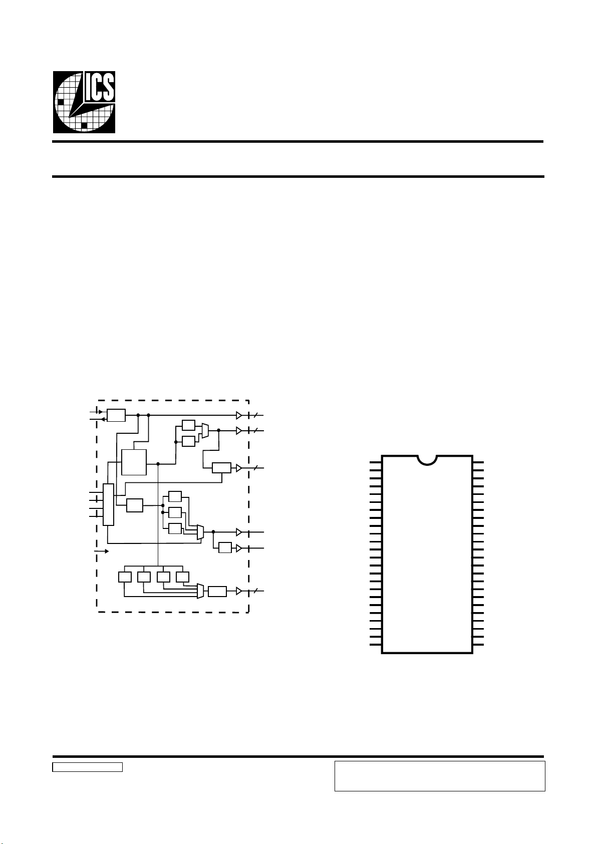
ICS9341
Block Diagram
133MHz Clock Generator and Integrated Buffer for PowerPC™
9341 Rev A 10/12/99
Pin Configuration
48-pin SSOP
* Internal pull-up resistor of 120K to 3.3V on
indicated inputs
** Internal pull-down resistor of 120K to GND
on indicated inputs.
Generates the following system clocks:
- 4-CPUA (3.3V, up to 133MHz)
- 4-CPUB (3.3V, up to 133MHz)
- 8-PCI (3.3V, 33.3MHz)
- 1-OUT (3.3v, 64MHz)
- 1-OUT/2 (3.3V, OUT/2MHz)
- 2-REF (3.3V, 14.318MHz)
Up to 133MHz frequency support.
Stop clocks for power management
Spread Spectrum for EMI control
±.25% center spread
Skew characteristics:
- CPU - CPU: <350ps
- CPU - PCI: <500ps
- PCI - PCI: <500ps
The ICS9341 generates all clocks required for high speed
PowerPC RISC microprocessor systems. Generating clocks in
phase with an external reference frequency.
Spread Spectrum may be enabled by driving the SS_EN pin
active. Spread spectrum typically reduces system EMI by 8dB
to 10dB. This simplifies EMI qualification without resorting to
board design iterations or costly shielding. The ICS9341
employs a proprietary closed loop design, which tightly
controls the percentage of spreading over process and
temperature variations.
Power Groups:
VDDREF, GNDREF = REF, X1, X2
GNDPCI, VDDPCI = PCICLK
VDD66, GND66 = 3V66
VDD48, GND48 = 48MHz
VDDCOR, GNDCOR = PLL Core
VDDLCPU/2 , GNDLCPU/2 = CPU/2
VDDLIOAPIC, GNDIOAPIC = IOAPIC
PD#
CPUB_STOP#
OUT_SEL (0:1)
PCI_STOP#
SS_EN
X1
X2
OSC
PLL
Spread
Spectrum
REF (0:1)
2
4
4
OUT
OUT/2
CPUCLKB (1:4)
CPUCLKA (1:4)
STOP
C
o
n
t
r
o
l
/ 2
PLL2
8
PCICLK (1:8)
STOP
/ 8/ 6/ 5/ 4
/ 2
/ 4
/ 5
/ 6
/ 3
GNDREF
X1
X2
VDDPCI
PCICLK1
PCICLK2
PCICLK3
PCICLK4
GNDPCI
GNDCPUB
CPUB1
CPUB2
CPUB3
CPUB4
VDDCPUB
VDDPCI
PCICLK5
PCICLK6
PCICLK7
PCICLK8
FS0
FS1
*OUT_SEL0
GNDPCI
REF1
REF0
VDDREF
CPUA1
CPUA2
SS_EN
GNDCPUA
OUT_SEL1*
PD#
VDDCPUA
CPUA3
CPUA4
CPUB_STOP#**
VDDD
VDDOUT
OUT
OUT/2
GNDOUT
GNDA
GNDD
N/C
N/C
*PCI_STOP#
VDDA
ICS9341
1
2
3
4
5
6
7
8
9
10
11
12
13
14
15
16
17
18
19
20
21
22
23
24
48
47
46
45
44
43
42
41
40
39
38
37
36
35
34
33
32
31
30
29
28
27
26
25
ICS reserves the right to make changes in the device data identified in
this publication without further notice. ICS advises its customers to
obtain the latest version of all device data to verify that any
information being relied upon by the customer is current and accurate.
Page 2
2
ICS9341
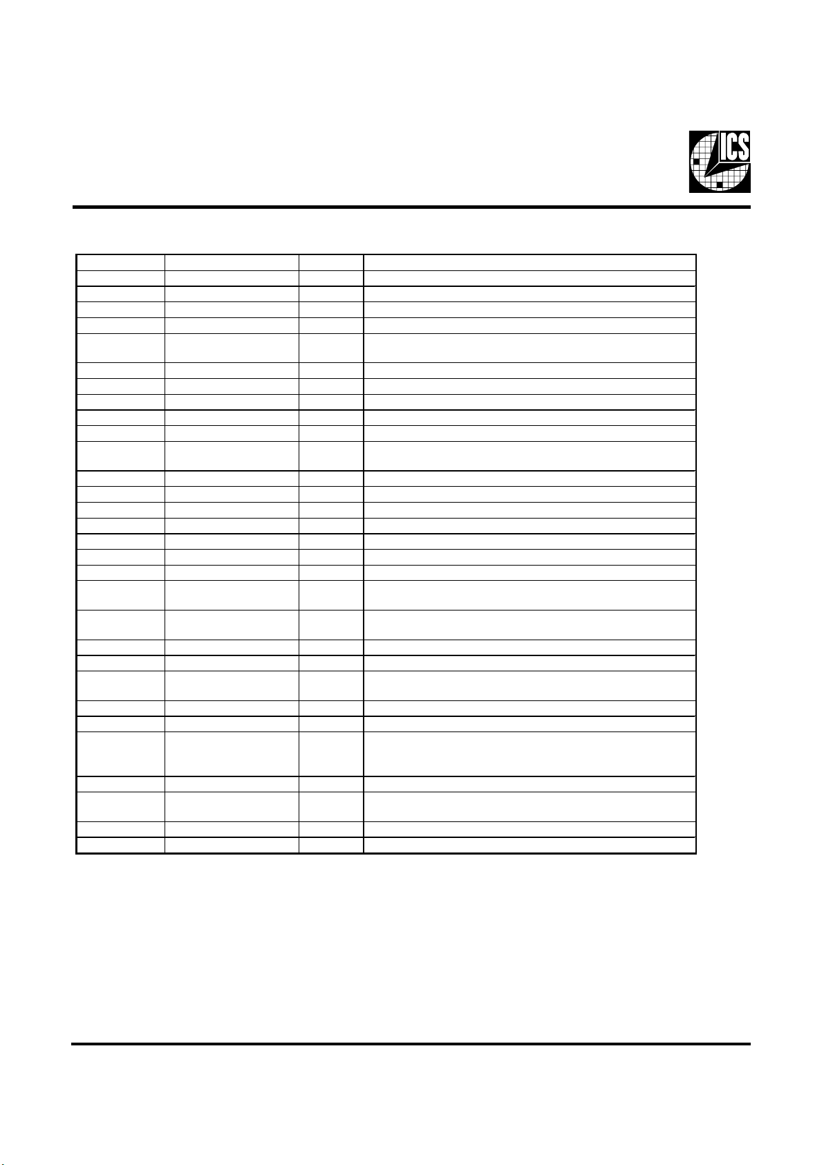
Pin Descriptions
Pin number Pin name Type Description
1 GNDREF PWR Ground pin for REF clocks.
2 X1 IN X T AL _IN 14 .318MHz c r ys tal input.
3 X2 OUT XTAL_OUT Crystal output.
4, 16 VDDPCI PWR 3.3Volts pow er pin for PCICLKs.
5, 6, 7, 8, 17, 18,
19, 20
PCIC LK (1:8) OUT PCI clock output at 3.3V. Syn chronous to CPU clocks.
9, 24 GNDPCI PWR Ground pin for PCI clocks.
10 GN DC P UB PWR G roun d pin for CP UB clocks.
11, 12, 13, 14 CPUB (1:4) OUT C P U C LK outputs up to 133.3MH z.
15 VD DC P UB PWR P ower pin for the CPU bank B C LK s . 3.3V .
21, 22 FS (0 :1) IN Logic - input for frequency selection.
23, 41 *OUT_SEL (0:1) IN
The se contr o l the o u tpu t func tionality of the OUT an d OUT /2 pins.
Refer to table for details.
24 GNDPC I P W R Gnd pin for P CICLKs.
25 VDDA PW R P ower for analog outputs.
26 *PCI_STOP# IN This active low input s tops PCI clocks.
27, 28 N/C - Not connected
29 GND D PWR Digitial ground
30 GN DA PW R A nalog ground
31 GN DOUT PWR G roun d for output pins.
32 OUT/2 O UT
H alf t he OUT frequ e ncy. Depe nd e nt on O U T _SE L. Refer to ta ble
fo r deta ils.
33 OUT OUT
This o utput fre que n c y is d epen den t o n OUT_SEL. Ref er to table f or
details.
34 VD DOUT PWR P ower for OU T pins 3.3V.
35 VD DD PW R Power for digitial outputs.
36 CPUB_S TO P #* * IN
This ac tive lo w in p ut sto p s the CP UB clock s at a log ic " 0 " level
when in
p
ut low .
45, 44, 38, 37 CPUA (1:4) O UT CP U CLK outputs up to 133.3MH z.
39 VD DC P UA PWR Pow er pin for the CPU bank A CLKs. 3.3V .
40 PD # IN
This asynchronous input powers down the chip when drive
active(Lo w) . T h e in ternal PL L s are d isabled an d all the ou tput clocks
are held at a Low state.
42 GN DC P UA PWR Ground pin for CP UB clocks.
43 SS_ EN IN
Sp r e ad spectr u m is turn ed on by d r iv ing this in p ut high and tur ned
off b
y
driving low.
46 VD DR EF PW R P ower pin for REF clocks.
47, 48 REF OU T 14.318MHz reference clock outputs at 3.3V.
Page 3
3
ICS9341
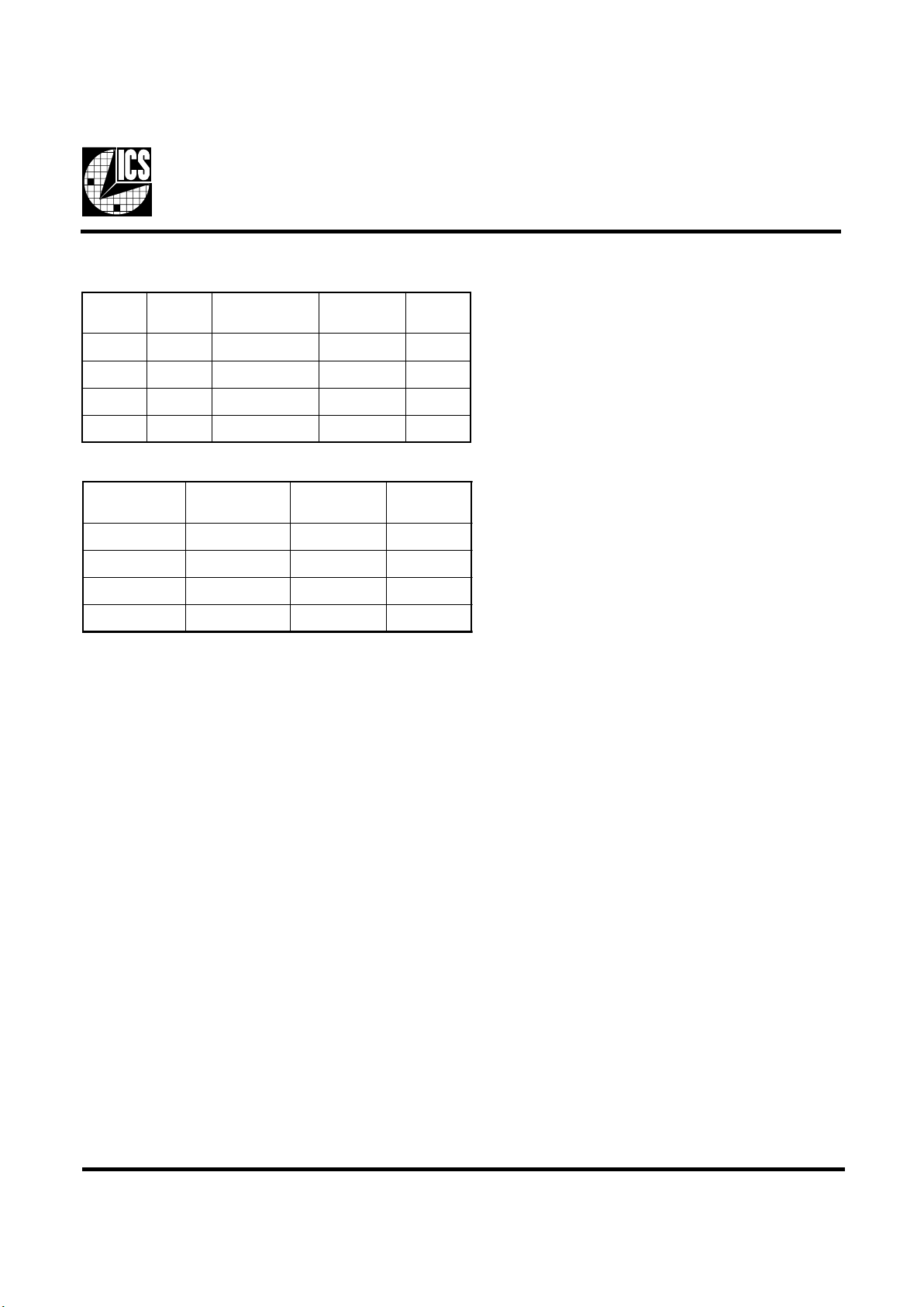
Frequency Selection
1SF0SF
BUPC,AUPC
)zHM(
ICP
)zHM(
FER
)zHM(
11 3.3313.33813.41
10 0013.33813.41
01 3.383.33813.41
00 6.663.33813.41
1LES_TUO0LES_TUO
TUO
)zHM(
2/TUO
)zHM(
118442
100402
014623
00 deppotSdeppotS
Page 4

4
ICS9341
PD# Timing Diagram
The power down selection is used to put the part into a very low power state without turning off the power to the part. PD# is
an asynchronous active low input. This signal needs to be synchronized internal to the device prior to powering down the clock
synthesizer.
Internal clocks are not running after the device is put in power down. When PD# is active low all clocks need to be driven to a
low value and held prior to turning off the VCOs and crystal. The power up latency needs to be less than 3 mS. The power down
latency should be as short as possible but conforming to the sequence requirements shown below. The REF and 48MHz clocks
are expected to be stopped in the LOW state as soon as possible. Due to the state of the internal logic, stopping and holding
the REF clock outputs in the LOW state may require more than one clock cycle to complete.
Notes:
1. All timing is referenced to the Internal CPUCLK (defined as inside the ICS9341 device).
2. As shown, the outputs Stop Low on the next falling edge after PD# goes low.
3. PD# is an asynchronous input and metastable conditions may exist. This signal is synchronized inside this part.
4. The shaded sections on the VCO and the Crystal signals indicate an active clock.
5. Diagrams shown with respect to 133MHz. Similar operation when CPU is 100MHz.
Page 5

5
ICS9341
PCI_STOP# Timing Diagram
PCI_STOP# is an input to the clock synthesizer. It is used to turn off the PCI clocks for low power operation. PCI clocks are
required to be stopped in a low state and started such that a full high pulse width is guaranteed. ONLY one rising edge of
PCICLK_F is allowed after the clock control logic switched for the PCI outputs to become enabled/disabled.
Notes:
1. All timing is referenced to CPUCLK.
2. Internal means inside the chip.
3. All other clocks continue to run undisturbed.
4. PD# and CPU_STOP# are shown in a high state.
CPU_STOP# Timing Diagram
CPU_STOP# is an asynchronous input to the clock synthesizer. It is used to turn off the CPU and 3V66 clocks for low power
operation. CPU_STOP# is asserted asynchronously by the external clock control logic with the rising edge of free running PCI
clock (and hence CPU clock) and must be internally synchronized to the external output. All other clocks will continue to run
while the CPU clocks are disabled. The CPU clocks must always be stopped in a low state and started in such a manner as to
guarantee that the high pulse width is a full pulse.
Notes:
1. All timing is referenced to the internal CPUCLK.
2. The internal label means inside the chip and is a reference only. This in fact may not be the way that the control is designed.
3. PD# and PCI_STOP# are shown in a high state.
Page 6

6
ICS9341
Absolute Maximum Ratings
Supply Voltage . . . . . . . . . . . . . . . . . . . . . . . . . . . 7.0 V
Logic Inputs . . . . . . . . . . . . . . . . . . . . . . . . . . . . GND 0.5 V to VDD +0.5 V
Ambient Operating Temperature . . . . . . . . . . . . 0°C to +70°C
Storage Temperature . . . . . . . . . . . . . . . . . . . . . . 65°C to +150°C
Stresses above those listed under Absolute Maximum Ratings may cause permanent damage to the device. These ratings are
stress specifications only and functional operation of the device at these or any other conditions above those listed in the
operational sections of the specifications is not implied. Exposure to absolute maximum rating conditions for extended periods
may affect product reliability.
Electrical Characteristics - I nput/ Supply/Common Output Parameters
TA = 0 - 70º C; Supply Voltage VDD = V
DDL
= 3.3 V +/-5% (unless otherwise stated)
PARAMETER SYMBOL CONDITIONS MIN TYP MAX UNITS
Input High Voltage
V
IH
2
V
DD
+0.3
V
Input Low Voltage
V
IL
VSS-0.3
0.8 V
Input High Current
I
IH
VIN = V
DD
0.1 5
µA
Input Low Current
I
IL1
VIN = 0 V; Inputs with no pull-up resistors
-5 2.0
µA
Input Low Current
I
IL2
VIN = 0 V; Inputs with pull-up resistors
-200 -100
µA
I
DD3.3OP66
Select @ 66MHz; Max discrete cap loads 215 250 mA
I
DD3.3OP83
Select @ 83MHz; Max discrete cap loads 200 225 mA
I
DD3.3OP100
Select @ 100MHz; Max discrete cap loads 180 200 mA
I
DD3.3OP133
Select @ 133MHz; Max discrete cap loads 160 175 mA
Power Down Supply
Curren
t
I
DD3.3PD
PD# = 0
160 300
µA
Input frequency
F
i
VDD = 3.3 V
12 14.318 16 MHz
C
IN
Logic Inputs 5 pF
C
INX
X1 & X2 pins 13.5 18 22.5 pF
Transition Time
1
T
Trans
To 1st crossing of target Freq. 3 ms
Settlin
g
Time
1
T
S
From 1st crossing to 1% target Freq. 1 ms
Clk Stabilization
1
T
STAB
From VDD = 3.3 V to 1% target Freq.
3ms
Skew
1
t
CPUA-CPUBVT
= 1.5 V
100 350 ps
Skew
1
t
CPU-PCI
VT = 1.5 V
500 800 ps
Operating Supply
Current
Input Capacitance
1
Page 7

7
ICS9341
Electrical Characteristics - CPUA
TA = 0 - 70º C; VDD = V
DDL
= 3.3 V +/-5%; CL = 20 pF (unless otherwise stated)
PARAMETER SYMBOL CONDITIONS MIN TYP MAX UNITS
Output High Voltage V
OH2B
IOH = -8.0 mA 2 2.4 V
Output Low Voltage V
OL2B
IOL = 12 mA 0.32 0.4 V
Output High Current I
OH2B
VOH =1.7 V -37 -16 m A
Output Low Current I
OL2B
VOL = 0.7 V 19 26 mA
Rise Time t
r2B
1
VOL = 0.4 V, VOH = 2.4 V 1.5 2.5 ns
Fall Time t
f2B
1
VOH = 2.4 V, VOL = 0.4 V 1 2.5 ns
Duty Cycle d
t2B
1
VT = 1.5 V 40 50 55 %
Skew t
sk2B
1
VT = 1.5 V 125 175 ps
Jitter, Cycle-to-cycle
tj
cyc-cyc2B
1
VT = 1.5 V 230 350 ps
1
Guaranteed by design, not 100% tested in production.
Electrical Characteristics - CPUB
TA = 0 - 70º C; VDD = V
DDL
= 3.3 V +/-5%; CL = 30 pF (unless otherwise stated)
PARAMETER SYMBOL CONDITIONS MIN TYP MAX UNITS
Output High Voltage V
OH2B
IOH = -8.0 mA 2 2.4 V
Output Low Voltage V
OL2B
IOL = 12 mA 0.32 0.4 V
Output High Current I
OH2B
VOH =1.7 V -37 -16 m A
Output Low Current I
OL2B
VOL = 0.7 V 19 26 mA
Rise Time t
r2B
1
VOL = 0.4 V, VOH = 2.4 V 1.9 3 ns
Fall Time t
f2B
1
VOH = 2.4 V, VOL = 0.4 V 1.6 3 ns
Duty Cycle d
t2B
1
VT = 1.5 V 40 49 55 %
Skew t
sk2B
1
VT = 1.5 V 90 175 ps
Jitter, Cycle-to-cycle
tj
cyc-cyc2B
1
VT = 1.5 V 230 350 ps
1
Guaranteed by design, not 100% tested in production.
Page 8

8
ICS9341
Electrical Characteristics - PCI
TA = 0 - 70º C; VDD = V
DDL
= 3.3 V +/-5%; CL =30 pF
PARAMETER SYMBOL CONDITIONS MIN TYP MAX UNITS
Output High Volt age V
OH1
IOH = -11 mA 2.4 3.1 V
Output Low Voltage V
OL1
IOL = 9.4 mA 0.17 0.4 V
Output High Current I
OH1
VOH = 2.0 V -60 -22 mA
Output Low Current I
OL1
VOL = 0.8 V 25 47 mA
Rise Time
1
t
r1
VOL = 0.4 V, VOH = 2.4 V 0.5 1.8 2.5 ns
Fall Time
1
t
f1
VOH = 2.4 V, VOL = 0.4 V 0.5 1.7 2.5 ns
Duty Cycle
1
d
t1
VT = 1.5 V 45 50 55 %
Skew
1
t
sk1
VT = 1.5 V 150 500 ps
Jitter, Cycle-to-cycle
1
t
jcyc-cyc1
VT = 1.5 V
120 500 ps
1
Guaranteed by design, not 100% tested in production.
Electrical Characteristics - REF, OUT, OUT/2
TA = 0 - 70º C; VDD = V
DDL
= 3.3 V +/-5%; CL = 20 pF (unless otherwise state d)
PARAMETER SYMBOL CONDITIONS MIN TYP MAX UNITS
Output High Voltage V
OH5
IOH = -12 mA 2.4 2.9 V
Output Low Voltage V
OL5
IOL = 10 mA 0.33 0.4 V
Output High Current I
OH5
VOH = 2.0 V -30 -20 mA
Output Low Current I
OL5
VOL = 0.8 V 16 23 mA
Rise Time
1
t
r5
VOL = 0.4 V, VOH = 2.4 V; OUT 1.5 1.8 4 ns
Fall Time
1
t
f5
VOH = 2.4 V, VOL = 0.4 V; OUT 1.5 2 4 ns
Duty Cycle
1
d
t5
VT = 1.5 V; OUT 45 52 55 %
Rise Time
1
t
r5
VOL = 0.4 V, VOH = 2.4 V; OUT/2 1.5 2.2 4 ns
Fall Time
1
t
f5
VOH = 2.4 V, VOL = 0.4 V; OUT/2 1.5 2.1 4 ns
Duty Cycle
1
d
t5
VT = 1.5 V; OUT/2 45 50 55 %
Rise Time
1
t
r5
VOL = 0.4 V, VOH = 2.4 V; REF 1.5 2.7 4 ns
Fall Time
1
t
f5
VOH = 2.4 V, VOL = 0.4 V; REF 1.5 2.8 4 ns
Duty Cycle
1
d
t5
VT = 1.5 V; REF 45 50 55 %
Jitter, Cycle-to-cycle1 t
jcy
c-cyc5
VT = 1.5 V; OUT, OUT/2 280 500 ps
Jitter, Cycle-to-cycle
1
t
jcyc-cyc5
VT = 1.5 V; REF
450 1000 ps
1
Guaranteed by design, not 100% tested in production.
Page 9

9
ICS9341
SSOP Package
SYM BOL CO MM ON DIMENSIO NS VARIATIONS D N
MIN. NOM. MAX. MIN. NOM. MAX.
A .095 .101 .110 AC .620 .625 .630 48
A1 .008 .012 .016
A2 .088 .090 .092
B .008 .010 .0135
C .005 - .010
D See Variations
E .292 .296 .299
e 0.025 BSC
H .400 .406 .410
h .010 .013 .016
L .024 .032 .040
N See Variations
µ
0° 5° 8°
X .085 .093 .100
ICS reserves the right to make changes in the device data identified in
this publication without further notice. ICS advises its customers to
obtain the latest version of all device data to verify that any
information being relied upon by the customer is current and accurate.
Ordering Information
ICS9341yF
Pattern Number (2 or 3 digit number for parts with ROM code patterns)
Package Type
F=SSOP
Revision Designator (will not correlate with datasheet revision)
Device Type (consists of 3 or 4 digit numbers)
Prefix
ICS, AV = Standard Device
Example:
ICS XXXX y F - PPP
 Loading...