

Page 1
ICS9250-32
Third party brands and names are the property of their respective owners.
Integrated
Circuit
Systems, Inc.
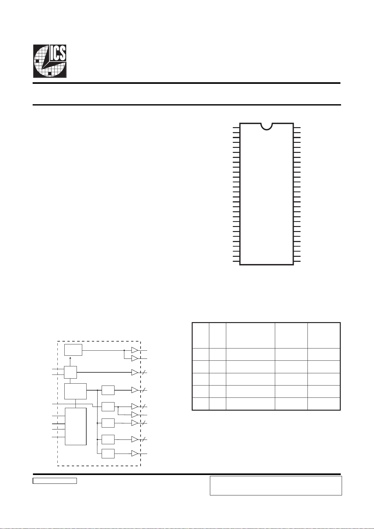
Block Diagram
9250-32 Rev B 9/7/00
Recommended Application:
Timna Style Chipset
Output Features:
• 3 - CPUs @ 2.5V
• 8 - PCI @ 3.3V
• 2 - IOAPIC @ 2.5V
• 1 - MREF @ 2.5V, DRCG memory reference clock
• 9 - SDRAM @ 3.3V including one free running
• 1 - 2V48M @ 2.5V fixed (DOT)
• 1 - 3V48M @ 3.3V fixed (USB)
• 2 - REF @ 3.3V, 14.318MHz.
Features:
• Support power management: CPU, PCI, SDRAM stop
from I
2
C programming.
• Spread spectrum for EMI control (0 to -0.5%)
• Uses external 14.318MHz crystal
Key Specifications:
• CPU Output Jitter
(Cyc-Cyc)
: <175ps
• IOAPIC Output Jitter
(Cyc-Cyc)
: <500ps
• MREF Output Jitter
(Cyc-Cyc)
: <250ps
• 2V48M Output Jitter
(Cyc-Cyc)
: <250ps
• 3V48M Output Jitter
(Cyc-Cyc)
: <500ps
• CPU - CPU: < 175ps
• SDRAM - SDRAM < 250ps
• PCI - PCI: < 500ps
• IOAPIC - IOAPIC: < 250ps
• BUFFER_IN to SDRAM prop delay: 5.5 to 7.5ns
Functionality
Pin Configuration
56-Pin 300mil SSOP
* These inputs have a 50K pull up to VDD.
Frequency Generator & Integrated Buffers for PII/III™
2V48M
3V48M
VDD48
GND48
X1
X2
GND
*(CPU2_EN#)REF0
REF1
VDD
PCICLK0
PCICLK1
GNDPCI
VDDPCI
PCICLK2
PCICLK3
PCICLK4
PCICLK5
VDDPCI
GNDPCI
PCICLK6
PCICLK7
SCLK
VDDA
GNDA
S DATA
BUF_IN
*FS0
VDDLIOAPIC
IOAPIC0
IOAPIC1
GNDLIOAPIC
VDDLCPU
CPUCLK0
CPUCLK1
VDDLCPU
GNDLCPU
CPUCLK2
MREF66
VDD
SDRAM_F
SDRAM0
VDDSDR
GNDSDR
SDRAM1
SDRAM2
SDRAM3
GNDSDR
VDDSDR
SDRAM4
SDRAM5
VDDSDR
GNDSDR
SDRAM6
SDRAM7
FS1*
ICS9250-32
1
2
3
4
5
6
7
8
9
10
11
12
13
14
15
16
17
18
19
20
21
22
23
24
25
26
27
28
56
55
54
53
52
51
50
49
48
47
46
45
44
43
42
41
40
39
38
37
36
35
34
33
32
31
30
29
PLL2
PLL1
Spread
Spectrum
3V48M
2V48M
CPUCLK (2:0)
SDRAM (7:0)
IOAPIC (1:0)
PCICLK (7:0)
8
8
3
2
2
SDRAM_F
MREF66
X1
X2
XTAL
OSC
CPU
DIVDER
SDRAM
DIVDER
IOAPIC
DIVDER
PCI
DIVDER
3V66
DIVDER
REF (1:0)
CPU_EN#
BUF_IN
S DATA
SCLK
FS (1:0)
Control
Logic
Config.
Reg.
1SF0SF
dehctaLpurewoP
#NE_2UPC/1FER
0UPC
,1UPC
FERM
2UPC
11 1 zHM66etatsirT
11 0 zHM66zHM66
10 X 2/KLCT2/KLCT
01 X devreseRdevreseR
00 X etatsirTetatsirT
Power Groups
VDD = REF, X1, X2
VDDPCI = PCICLK
VDDSDR = SDRAM
VDD48 = 3V48M
VDDLCPU = CPU
VDDLIOAPIC = IOAPIC, 2V48M
VDDA = PLL Core
ICS reserves the right to make changes in the device data identified in
this publication without further notice. ICS advises its customers to
obtain the latest version of all device data to verify that any
information being relied upon by the customer is current and accurate.
Page 2
2
ICS9250-32
Third party brands and names are the property of their respective owners.
Functionality
The ICS9250-32 is the single chip clock solution for Desktop designs. It provides all necessary clock signals for such a system.
Spread spectrum may be enabled through I
2
C programming. Spread spectrum typically reduces system EMI by 8dB to 10dB.
This simplifies EMI qualification without resorting to board design iterations or costly shielding. The ICS9250-32 employs a
proprietary closed loop design, which tightly controls the percentage of spreading over process and temperature variations.
Serial programming I
2
C interface allows changing functions, stop clock programming and frequency selection.
General Description
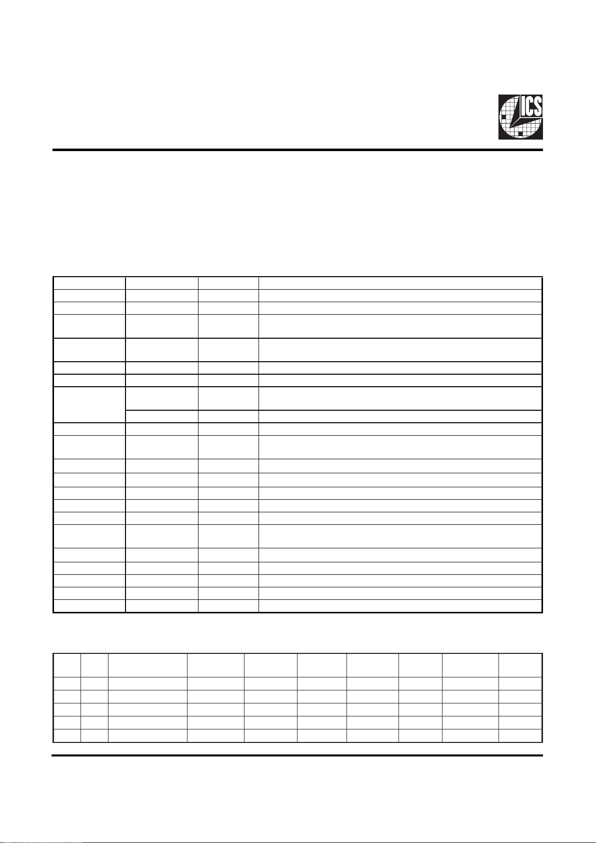
Pin Configuration
PIN NUMBER PIN NAME TYPE DESCRIPTION
1
2V48M OUT 48MHz output clock 2.5V (DOT) clock
2 3V48M OUT 48MHz output clock 3.3V (USB) clock
3, 10, 14, 19, 24,
33, 36, 42, 45
VDD PWR
3.3V Power supply for SDRAM output buffers, PCI output buffers,
reference out
p
ut buffers and 3V48 outpu
t
4, 7, 13, 20, 25,
32, 37, 41, 48, 53
GND PWR Ground pins
5 X1 IN Crystal input,nominally 14.318MHz.
6 X2 OUT Crystal output, nominally 14.318MHz.
CPU2_EN# IN
Disables CPU2 when pulled high (default)
Enables CPU2 when
p
ulled Low
REF0 OUT 14.318 MHz reference clock.
9 REF1 OUT 14.318 MHz reference clock.
22, 21, 18, 17, 16,
15, 12, 11
PCICLK (7:0) OUT PCI clock outputs.
23 SCLK IN
Clock
p
in of I2C circuitry 5V tolerant
26 SDATA I/O
Data
p
in for I2C circuitry 5V tolerant
27 BUF_IN IN Input to fan out buffer for SDRAM
28 FS0 IN Frequency select pin.
29 FS1 IN Frequency select pin.
30, 31, 34, 35, 38,
39, 40, 43
SDRAM (7:0) OUT SDRAM clock outputs
44 SDRAM_F OUT
SDRAM clock out
p
ut free running not affected by I2C
46 MREF66 OUT DRCG reference memory 2.5V 66MHz
49, 52, 56 VDDL PWR Power pins for CPUCLKs, and IOAPIC clocks. 2.5V
47, 50, 51 CPUCLK (2:0) OUT 2.5V CPU clock outputs.
54, 55 IOAPIC (1:0) OUT 2.5V IOAPIC clock outputs
8
1SF0SF
dehctaLpurewoP
#NE_2UPC/1FER
0UPC
FERM,1UPC
2UPC
MARDS
]7:0[
:84V2
84V3
ICPFERCIPAOI
11 1 zHM66etatsirTNI_FUBzHM84zHM33zHM813.41zHM33
11 0 zHM66zHM66NI_FUBzHM84zHM33zHM813.41zHM33
10 X 2/KLCT2/KLCTNI_FUB2/KLCT4/KLCTKLCT4/KLCT
01 X devreseRdevreseRdevreseRdevreseRdevreseRdevreseRdevreseR
00 X etatsirTetatsirTetatsirTetatsirTetatsirTetatsirTetatsirT
Page 3
3
ICS92 50-32
Third party brands and names are the property of their respective owners.
1. The ICS clock generator is a slave/receiver, I2C component. It can read back the data stored in the latches for
verification. Read-Back will support Intel PIIX4 "Block-Read" protocol.
2. The data transfer rate supported by this clock generator is 100K bits/sec or less (standard mode)
3. The input is operating at 3.3V logic levels.
4. The data byte format is 8 bit bytes.
5. To simplify the clock generator I
2
C interface, the protocol is set to use only "Block-Writes" from the controller. The
bytes must be accessed in sequential order from lowest to highest byte with the ability to stop after any complete byte
has been transferred. The Command code and Byte count shown above must be sent, but the data is ignored for those
two bytes. The data is loaded until a Stop sequence is issued.
6. At power-on, all registers are set to a default condition, as shown.
General I2C serial interface information
The information in this section assumes familiarity with I2C programming.
For more information, contact ICS for an I
2
C programming application note.
How to Write:
Controller (host) sends a start bit.
Controller (host) sends the write address D2
(H)
ICS clock will acknowledge
Controller (host) sends a dummy command code
ICS clock will acknowledge
Controller (host) sends a dummy byte count
ICS clock will acknowledge
Controller (host) starts sending first byte (Byte 0)
through byte 5
ICS clock will acknowledge each byte one at a time.
Controller (host) sends a Stop bit
How to Read:
Controller (host) will send start bit.
Controller (host) sends the read address D3
(H)
ICS clock will acknowledge
ICS clock will send the byte count
Controller (host) acknowledges
ICS clock sends first byte (Byte 0) through byte 5
Controller (host) will need to acknowledge each byte
Controller (host) will send a stop bit
Notes:
Controller (Host) ICS (Slave/Receiver)
Start Bit
Address
D3
(H)
AC
K
Byte Count
ACK
Byte
0
ACK
Byte 1
ACK
Byte
2
ACK
Byte
3
ACK
Byte 4
ACK
Byte
5
ACK
Stop Bit
How to Read:
Controller (Host) ICS (Slave/Receiver)
Start Bit
Address
D2
(H)
AC
K
Dummy Command Code
AC
K
Dummy Byte Count
AC
K
Byte 0
AC
K
Byte 1
ACK
Byte 2
AC
K
Byte 3
AC
K
Byte 4
AC
K
Byte 5
AC
K
Stop Bit
How to Write:
Page 4
4
ICS9250-32
Third party brands and names are the property of their respective owners.
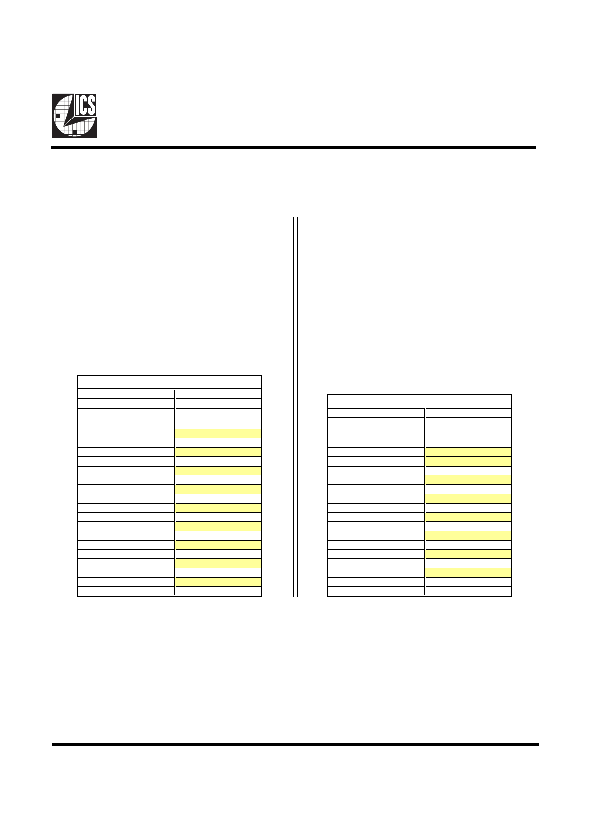
Byte 0: Active/Inactive Control Register
(1= enable, 0 = disable)
Byte 1: Active/Inactive Control Register
(1= enable, 0 = disable)
TIB#NIPDWPNOITPIRCSED
7tiB031 7MARDS
6tiB131 6MARDS
5tiB431 5MARDS
4tiB531 4MARDS
3tiB831 3MARDS
2tiB931 2MARDS
1tiB041 1MARDS
0tiB341 0MARDS
Notes:
1. Inactive means outputs are held LOW and are disabled
from switching.
2. Latched Frequency Selects (FS#) will be inverted logic
load of the input frequency select pin conditions.
TIB#NIPDWPNOITPIRCSED
7tiB-0 devreseR
6tiB-><devreseR
5tiB-><devreseR
4tiB-><devreseR
3tiB-0 devreseR
2tiB-0 devreseR
1tiB-0 devreseR
0tiB-0 devreseR
Byte 3: Active/Inactive Control Register
(1= enable, 0 = disable)
TIB#NIPDWPNOITPIRCSED
7tiB-0 devreseR
6tiB-0 devreseR
5tiB-0 devreseR
4tiB-0 devreseR
3tiB-0 devreseR
2tiB-0 devreseR
1tiB-0 devreseR
0tiB-0 devreseR
Byte 4: Active/Inactive Control Register
(1= enable, 0 = disable)
Byte 2: Active/Inactive Control Register
(1= enable, 0 = disable)
TIB#NIPDWPNOITPIRCSED
7tiB221 7KLCICP
6tiB121 6KLCICP
5tiB811 5KLCICP
4tiB711 4KLCICP
3tiB611 3KLCICP
2tiB511 2KLCICP
1tiB211 1KLCICP
0tiB111 0KLCICP
TIB#NIPDWPNOITPIRCSED
7tiB-0 devreseR
6tiB-0 devreseR
5tiB-0 devreseR
4tiB-0 devreseR
3tiB-0
murtcepSdaerpS
ffO=1/nO=0(
2tiB11 )TOD(M84V2
1tiB21 )BSU(M84V3
0tiB-1 devreseR
Note:
<>, with these 3 bits, the registers will store the written
values. The read back, however, will be the invert of the
written value.
Page 5

5
ICS92 50-32
Third party brands and names are the property of their respective owners.
Absolute Maximum Ratings
Supply Voltage . . . . . . . . . . . . . . . . . . . . . . . . . . . . 5.5 V
Logic Inputs . . . . . . . . . . . . . . . . . . . . . . . . . . . . . . GND 0.5 V to V
DD
+0.5 V
Ambient Operating Temperature . . . . . . . . . . . . . 0°C to +70°C
Case Temperature . . . . . . . . . . . . . . . . . . . . . . . . . . 115°C
Storage Temperature . . . . . . . . . . . . . . . . . . . . . . . 65°C to +150°C
Stresses above those listed under Absolute Maximum Ratings may cause permanent damage to the device. These ratings are
stress specifications only and functional operation of the device at these or any other conditions above those listed in the
operational sections of the specifications is not implied. Exposure to absolute maximum rating conditions for extended periods
may affect product reliability.
Electrical Characteristics - I nput/ Supply/Common Output Parameters
TA = 0 - 70C; Supply Voltage VDD = 3.3 V +/-5%, V
DDL
= 2.5 V +/-5% (unless otherwise stated)
PARAMETER SYMBOL CONDITIONS MIN TYP MAX UNITS
Input High Voltage V
IH
2V
DD
+0.3 V
Input Low Voltage V
IL
VSS-0.3 0.8 V
Input High Current I
IH
VIN = V
DD
-5 5
µA
I
IL1
VIN = 0 V; Inputs with no pull-up resistors -5
I
IL2
VIN = 0 V; Inputs with pull-up resistors -200
I
DD3.3OP
CL = Max loads;Select @ 66 MHz 251 280
mA
I
DD2.5OP
CL = Max loads;Select @ 66 MHz 27 100 mA
Input Frequency F
i
VDD = 3.3 V 14.312 MHz
C
IN
Logic Inputs 5 pF
C
INX
X1 & X2 oins 27 45 pF
Transition time
1
T
trans
To 1st crossing of target frequency 3 ms
Settling time
1
T
s
From 1st crossing to 1% target frequency 3 ms
Clk Stabilization
1
T
STAB
From VDD = 3.3 V to 1% target frequency 3 ms
T
CPU-IOAPIC
CPU & IOAPIC @ 1.25 V 1.5 2.3 3.5 ns
T
CPU-PCI
CPU @ 1.25 V, PCI @ 1.5 V 1.5 2.1 3.5 ns
1
Guaranteed by design, not 100% tested in production.
µA
Skew
1
Operating Supply
Current
Input Capacitance
Input Low Current
Page 6

6
ICS9250-32
Third party brands and names are the property of their respective owners.
Electrical Characteristics - CPU
TA = 0 - 70C; V
DDL
= 2.5 V +/-5%; CL = 10-20 pF (unless otherwise specified)
PARAMETER SYMBOL CONDITIONS MIN TYP MAX UNITS
Out
p
ut Impedance
1
R
DSP2B
VO = VDD*(0.5)
11.5 14 45
Ω
Out
p
ut Impedance
1
R
DSN2B
VO = VDD*(0.5)
11.5 16 45
Ω
Output High Voltage
V
OH2B
IOH = -1 mA
22.5 V
Output Low Voltage
V
OL2B
IOL = 1 mA
0.011 0.4 V
V
OH @ MIN
= 1.0 V
-79 -27
V
OH @ MAX
= 2.375 V
-27 -10
V
OL @ MIN
= 1.2 V
27 66
V
OL @ MAX
= 0.3 V
20 30
Rise Time
1
t
r2B
VOL = 0.4 V, VOH = 2.0 V
0.4 1.1 1.6 ns
Fall Time
1
t
f2B
VOH = 2.0 V, VOL = 0.4 V
0.4 1.1 1.6 ns
Duty Cycle
1
d
t2B
VT = 1.25 V
45 47 55 %
Skew window
1
t
sk2B
VT = 1.25 V
54 175 ps
Jitter, Cycle-to-cycle
1
t
jcyc-cyc2B
VT = 1.25 V
140 250 ps
1
Guaranteed by design, not 100% tested in production.
AC timing of the t
rise
& t
fall
is controlled by pre-driver circuit which allows lower impedance output to stay in the middle of
transition time target.
mA
mA
Output High Current
Output Low Current
I
OH2B
I
OL2B
Electrical Characteristics - PCI
TA = 0 - 70C; VDD = 3.3 V +/-5%; CL = 10-30 pF (unless otherwise specified)
PARAMETER SYMBOL CONDITIONS MIN TYP MAX UNITS
Output Impedance
1
R
DSP1B
VO = V
DD
*(0.5) 11 14 55 Ω
Output Impedance
1
R
DSN1B
VO = V
DD
*(0.5) 11 13 55 Ω
Output High Voltage V
OH1
IOH = -1 mA 2.4 3.29 V
Output Low Voltage V
OL1
IOL = 1 mA 0.009 0.55 V
V
OH @ MIN
= 1.0 V -111 -29
V
OH @ MAX
= 3.135 V -27 -12
V
OL @ MIN
= 1.95 V 29 96
V
OL @ MAX
= 0.4 V 31 27
Rise Time
1
t
r1
VOL = 0.4 V, VOH = 2.4 V 0.5 1.2 2 ns
Fall Time
1
t
f1
VOH = 2.4 V, VOL = 0.4 V 0.5 1.4 2 ns
Duty Cycle
1
d
t1
VT = 1.5 V 45 51 55 %
Skew window
1
t
sk1
VT = 1.5 V 212 500 ps
Jitter, Cycle-to-cycle
1
t
jcyc-cyc1
VT = 1.5 V
230 500 ps
1
Guaranteed by design, not 100% tested in production.
AC timing of the t
rise
& t
fall
is controlled by pre-driver circuit which allows lower impedance output to stay in the middle of
transition time target.
Output High Current
I
OH1
mA
Output Low Current
I
OL1
mA
Page 7

7
ICS92 50-32
Third party brands and names are the property of their respective owners.
Electrical Characteristics - 2V48M
TA = 0 - 70C; V
DDL
= 2.5 V +/-5%; CL = 10-20 pF (unless otherwise specified)
PARAMETER SYMBOL CONDITIONS MIN TYP MAX UNITS
Out
p
ut Impedance
1
R
DSP5
VO = VDD*(0.5)
9.5 45
Ω
Out
p
ut Impedance
1
R
DSN5
VO = VDD*(0.5)
9.5 45
Ω
Output High Voltage
V
OH5
IOH = -1 mA
22.5 V
Output Low Voltage
V
OL5
IOL = 1 mA
0.007 0.4 V
V
OH @ MIN
= 1.0 V
-93 -27
V
OH @ MAX
= 2.375 V
-27 -11
V
OL @ MIN
= 1.2 V
27 81
V
OL @ MAX
= 0.3 V
27 30
Rise Time
1
t
r5
VOL = 0.4 V, VOH = 2.0 V
0.4 0.7 1.6 ns
Fall Time
1
t
f5
VOH = 2.0 V, VOL = 0.4 V
0.4 0.7 1.6 ns
Duty Cycle
1
d
t5
VT = 1.25 V
45 53 55 %
Jitter, Cycle-to-cycle
1
t
jcyc-cyc5
VT = 1.25 V
180 250 ps
1
Guaranteed by design, not 100% tested in production.
Output High Current
I
OH5
mA
Output Low Current
I
OL5
mA
AC timing of the t
rise
& t
fall
is controlled by pre-driver circuit which allows lower impedance output to stay in the middle of
transition time target.
Electrical Characteristics - 3V48M
TA = 0 - 70C; VDD = 3.3 V +/-5%; CL = 10-15 pF (unless otherwise specified)
PARAMETER SYMBOL CONDITIONS MIN TYP MAX UNITS
Output Impedance
1
R
DSP5
VO = V
DD
*(0.5) 16 24 60 Ω
Output Impedance
1
R
DSN5
VO = VDD*(0.5) 16 60
Ω
Output High Voltage V
OH5
IOH = -1 mA 2.4 3.3 V
Output Low Voltage V
OL5
IOL = 1 mA 0.014 0.4 V
V
OH @ MIN
= 2.0 V -65 -27
V
OH @ MAX
= 3.135 V -23 -8
V
OL @ MIN
= 1.0 V 29 65
V
OL @ MAX
= 0.4 V 21 27
Rise Time
1
t
r5
VOL = 0.4 V, VOH = 2.4 V 0.5 1.2 2 ns
Fall Time
1
t
f5
VOH = 2.4 V, VOL = 0.4 V 0.5 1.6 2 ns
Duty Cycle
1
d
t5
VT = 1.5 V 45 54 55 %
Jitter, Cycle-to-cycle
1
t
jcyc-cyc5
VT = 1.5 V, CPU=66,100,133 MHz
290 500 ps
1
Guaranteed by design, not 100% tested in production.
Output High Current
I
OH5
mA
Output Low Current
I
OL5
mA
AC timing of the t
rise
& t
fall
is controlled by pre-driver circuit which allows lower impedance output to stay in the middle of
transition time target.
Page 8

8
ICS9250-32
Third party brands and names are the property of their respective owners.
Electrical Characteristics - SDRAM
TA = 0 - 70C; VDD = 3.3 V +/-5%; CL = 20-30 pF (unless otherwise specified)
PARAMETER SYMBOL CONDITIONS MIN TYP MAX UNITS
Output Impedance
1
R
DSP2A
VO = V
DD
*(0.5) 8.5 10.1 24 Ω
Output Impedance
1
R
DSN2A
VO = V
DD
*(0.5) 8.5 12 24 Ω
Output High Voltage V
OH2A
IOH = -1 mA 2.4 3.3 V
Output Low Voltage V
OL2A
IOL = 1 mA 0.006 0.4 V
V
OH @ MIN
= 2.0 V -100 -54
V
OH @ MAX
= 3.135 V -46 -13
V
OL @ MIN
= 1.0 V 53 90
V
OL @ MAX
= 0.4 V 40 54
Rise Time
1
t
r2A
VOL = 0.4 V, VOH = 2.4 V 0.4 1 1.6 ns
Fall Time
1
t
f2A
VOH = 2.4 V, VOL = 0.4 V 0.4 0.8 1.6 ns
Duty Cycle
1
d
t2A
VT = 1.5 V 45 51 55 %
Skew (ouput to output)
1
t
sk2A
VT = 1.5 V 212 250 ps
Skew (Buffer In to output)
1
t
sk2B
VT = 1.5 V
5.5 6.5 7.5 ns
1
Guaranteed by design, not 100% tested in production.
Output Low Current
I
OL2A
mA
Output High Current
I
OH2A
mA
AC timing of the t
rise
& t
fall
is controlled by pre-driver circuit which allows lower impedance output to stay in the middle of
transition time target.
Electrical Characteristics - REF
TA = 0 - 70C; VDD = 3.3 V +/-5%; CL = 10-15 pF (unless otherwise specified)
PARAMETER SYMBOL CONDITIONS MIN TYP MAX UNITS
Output Impedance
1
R
DSP5
VO = V
DD
*(0.5) 16 24 60 Ω
Output Impedance
1
R
DSN5
VO = VDD*(0.5) 16 19.2 60
Ω
Output High Voltage V
OH5
IOH = -1 mA 2.4 3.3 V
Output Low Voltage V
OL5
IOL = 1 mA 0.014 0.4 V
V
OH @ MIN
= 2.0 V -65 -27
V
OH @ MAX
= 3.135 V -23 -8
V
OL @ MIN
= 1.0 V 29 65
V
OL @ MAX
= 0.4 V 21 27
Rise Time
1
t
r5
VOL = 0.4 V, VOH = 2.4 V 1.4 4 ns
Fall Time
1
t
f5
VOH = 2.4 V, VOL = 0.4 V 1.4 4 ns
Duty Cycle
1
d
t5
VT = 1.5 V 45 54 55 %
Jitter, Cycle-to-cycle
1
t
jcyc-cyc5
VT = 1.5 V, CPU=66,100,133 MHz
674 1000 ps
1
Guaranteed by design, not 100% tested in production.
mA
Output High Current
I
OH5
mA
AC timing of the t
rise
& t
fall
is controlled by pre-driver circuit which allows lower impedance output to stay in the middle of
transition time target.
Output Low Current
I
OL5
Page 9

9
ICS92 50-32
Third party brands and names are the property of their respective owners.
Electrical Characteristics - IOAPIC
TA = 0 - 70C; V
DDL
= 2.5 V +/-5%; CL = 10-20 pF (unless otherwise specified)
PARAMETER SYMBOL CONDITIONS MIN TYP MAX UNITS
Output Impedance R
DSP4B
1
VO = V
DD
*(0.5) 13.5 16 45 Ω
Output Impedance R
DSN4B
1
VO = V
DD
*(0.5) 13.5 19 45 Ω
Output High Voltage V
OH4B
IOH = -1 mA 2 2.5 V
Output Low Voltage V
OL4B
IOL = 1 mA 0.013 0.4 V
V
OH @ MIN
= 1.0 V -68 -27
V
OH @ MAX
= 2.375 V -27 -9
V
OL @ MIN
= 1.2 V 27 54
V
OL @ MAX
= 0.3 V 20 30
Rise Time
1
t
r4B
VOL = 0.4 V, VOH = 2.0 V 0.4 1.2 1.6 ns
Fall Time
1
t
f4B
VOH = 2.0 V, VOL = 0.4 V, IOIAPIC=PCI/2
0.40.951.6 ns
Duty Cycle
1
d
t4B
VT = 1.25 V 45 48 55 %
Skew window
1
t
sk1
VT = 1.5 V 18 250 ps
Jitter, Cycle-to-cycle
1
t
jcyc-cyc4B
VT = 1.25 V
93 500 ps
1
Guaranteed by design, not 100% tested in production.
Output Low Current
I
OL4B
mA
Output High Current
I
OH4B
mA
Electrical Characteristics - MREF66
TA = 0 - 70C; V
DDL
= 2.5 V +/-5%; CL = 10-20 pF (unless otherwise specified)
PARAMETER SYMBOL CONDITIONS MIN TYP MAX UNITS
Out
p
ut Impedance
1
R
DSP2B
VO = VDD*(0.5)
11.5 14 45
Ω
Out
p
ut Impedance
1
R
DSN2B
VO = VDD*(0.5)
11.5 16 45
Ω
Output High Voltage
V
OH2B
IOH = -1 mA
22.5 V
Output Low Voltage
V
OL2B
IOL = 1 mA
0.011 0.4 V
V
OH @ MIN
= 1.0 V
-79 -27
V
OH @ MAX
= 2.375 V
-27 -10
V
OL @ MIN
= 1.2 V
27 66
V
OL @ MAX
= 0.3 V
20 30
Rise Time
1
t
r2B
VOL = 0.4 V, VOH = 2.0 V
0.4 1.1 1.6 ns
Fall Time
1
t
f2B
VOH = 2.0 V, VOL = 0.4 V
0.4 1.1 1.6 ns
Duty Cycle
1
d
t2B
VT = 1.25 V
45 47 55 %
Jitter, Cycle-to-cycle
1
t
jcyc-cyc2B
VT = 1.25 V
168 250 ps
1
Guaranteed by design, not 100% tested in production.
Output Low Current
I
OL2B
mA
AC timing of the t
rise
& t
fall
is controlled by pre-driver circuit which allows lower impedance output to stay in the middle of
transition time target.
Output High Current
I
OH2B
mA
Page 10

10
ICS9250-32
Third party brands and names are the property of their respective owners.
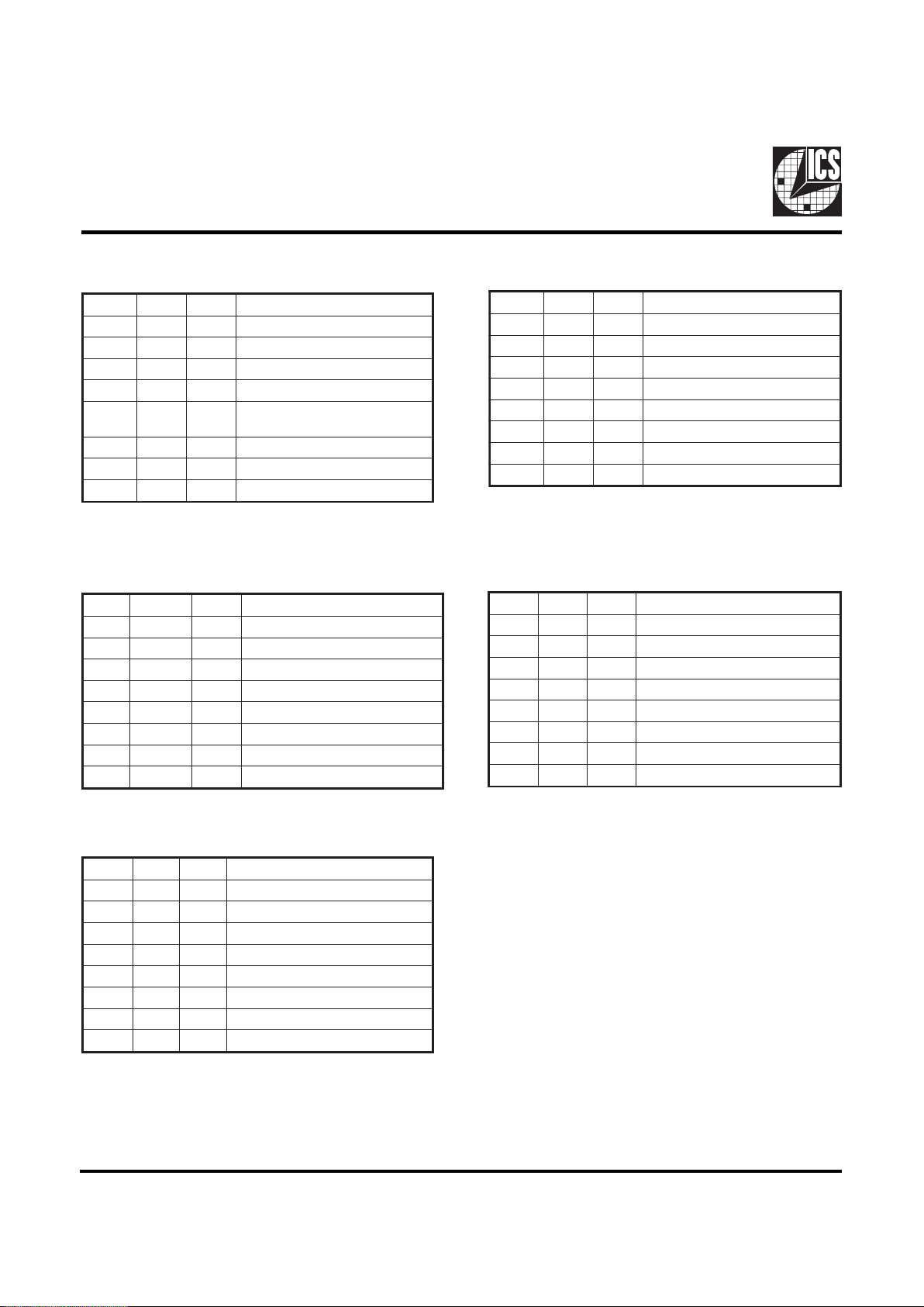
Fig. 1
Shared Pin Operation Input/Output Pins
The I/O pins designated by (input/output) on the ICS925032 serve as dual signal functions to the device. During initial
power-up, they act as input pins. The logic level (voltage)
that is present on these pins at this time is read and stored
into a 5-bit internal data latch. At the end of Power-On reset,
(see AC characteristics for timing values), the device changes
the mode of operations for these pins to an output function.
In this mode the pins produce the specified buffered clocks
to external loads.
To program (load) the internal configuration register for these
pins, a resistor is connected to either the VDD (logic 1) power
supply or the GND (logic 0) voltage potential. A 10 Kilohm
(10K) resistor is used to provide both the solid CMOS
programming voltage needed during the power-up
programming period and to provide an insignificant load on
the output clock during the subsequent operating period.
Via to
VDD
Clock trace to load
Series Term. Res.
Programming
Header
Via to Gnd
Device
Pad
2K
8.2K
Figure 1 shows a means of implementing this function when
a switch or 2 pin header is used. With no jumper is installed
the pin will be pulled high. With the jumper in place the pin
will be pulled low. If programmability is not necessary, than
only a single resistor is necessary. The programming resistors
should be located close to the series termination resistor to
minimize the current loop area. It is more important to locate
the series termination resistor close to the driver than the
programming resistor.
Page 11

11
ICS92 50-32
Third party brands and names are the property of their respective owners.
Ordering Information
ICS9250yF-32-T
Designation for tape and reel packaging
Pattern Number (2 or 3 digit number for parts with ROM code patterns)
Package Type
F=SSOP
Revision Designator (will not correlate with datasheet revision)
Device Type (consists of 3 or 4 digit numbers)
Prefix
ICS, AV = Standard Device
Example:
ICS XXXX y F - PPP - T
MIN MA X MIN MA X
A 2.413 2.794 .095 .110
A1 0.203 0.406 .008 .016
b 0.203 0.343 .008 .0135
c 0.127 0.254 .005 .010
D
E 10.033 10.668 .395 .420
E1 7.391 7.595 .291 .299
e 0.635 BASIC 0.025 BASIC
h 0.381 0.635 .015 .025
L 0.508 1.016 .020 .040
N
α
0° 8° 0° 8°
V A RIATIONS
MIN MA X MIN MA X
28 9.398
9.652
.370 .380
34 11.303
11.557
.445 .455
48 15.748
16.002
.620 .630
56 18.288
18.542
.720 .730
64 20.828
21.082
.820 .830
J E DE C MO- 118
DOC # 10-0034
6/1/00
REV B
SYMBOL
SEE VARIATIONS
SEE VARIATIONS
In Millimeter s
COMMON DIMENSIONS
In Inc h e s
COMMON DIMENSIONS
SEE VARIATIONS
N
D mm.
D (inch)
SEE VARIATIONS
ICS reserves the right to make changes in the device data identified in
this publication without further notice. ICS advises its customers to
obtain the latest version of all device data to verify that any
information being relied upon by the customer is current and accurate.
 Loading...