

Page 1
Integrated
Circuit
Systems, Inc.
ICS9250-23
Third party brands and names are the property of their respective owners.
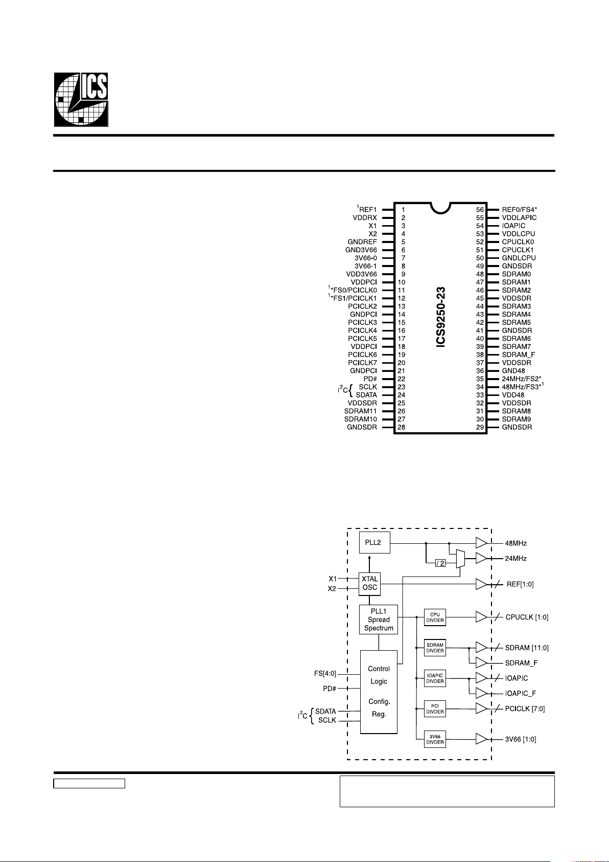
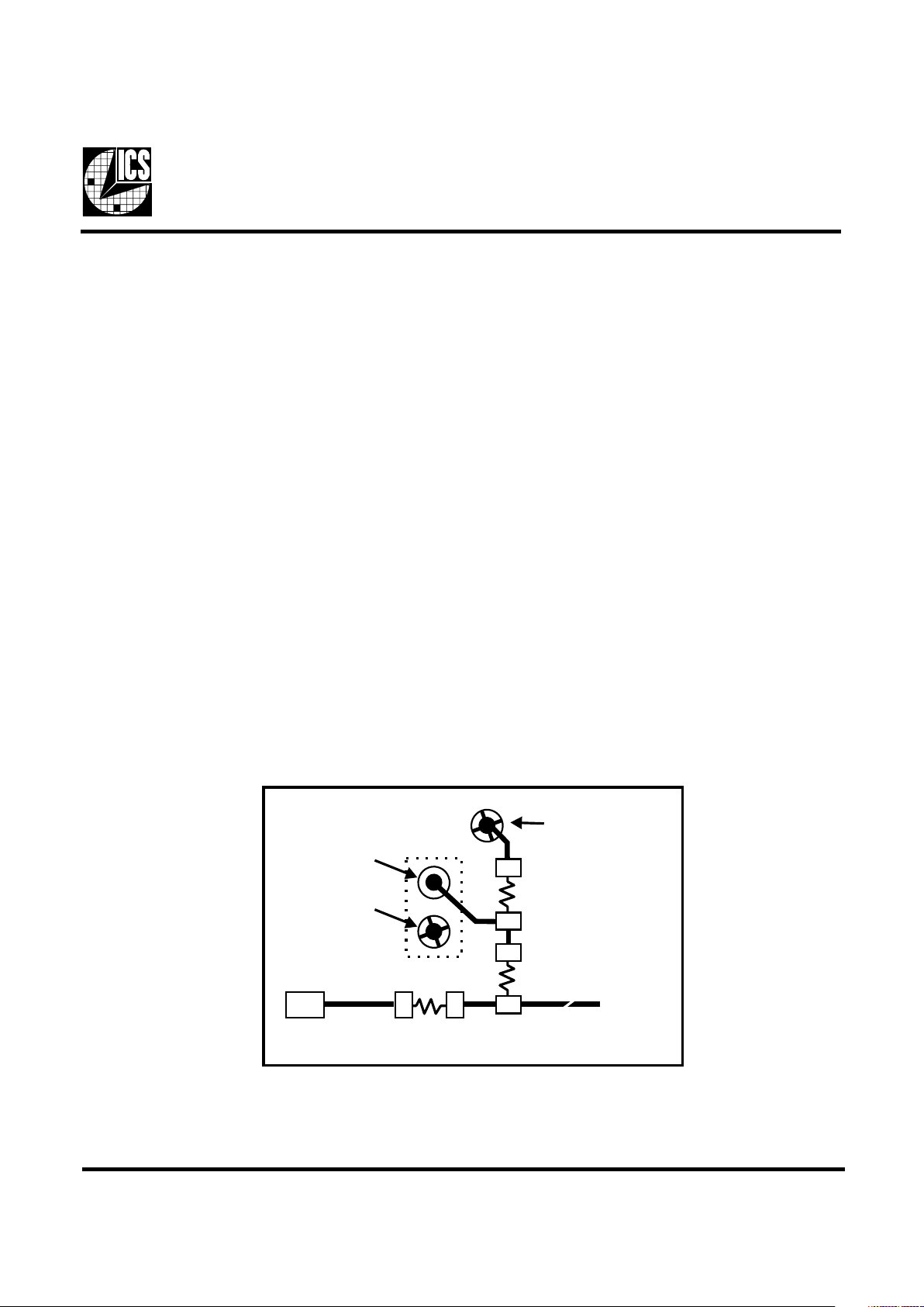
Block Diagram
9250-23 Rev A 4/3/01
Pin Configuration
Recommended Application:
810/810E type chipset
Output Features:
• 2 - CPUs @ 2.5V, up to 166MHz.
• 13 - SDRAM @ 3.3V, up to 166MHz.
• 2 - 3V66 @ 3.3V, 2x PCI MHz.
• 8 - PCI @3.3V.
• 1 - 48MHz, @3.3V fixed.
• 1 - 24MHz @ 3.3V
• 2 - REF @3.3V, 14.318MHz.
Features:
• Up to 166MHz frequency support
• Support power management through PD#.
• Spread spectrum for EMI control (± 0.25%)
center spread.
• Uses external 14.318MHz crystal
• FS pins for frequency select
Key Specifications:
• CPU Output Jitter: <250ps
• IOAPIC Output Jitter: <500ps
• 48MHz, 3V66, PCI Output Jitter: <500ps
• Ref Output Jitter. <1000ps
• CPU Output Skew: <175ps
• PCI Output Skew: <500ps
• 3V66 Output Skew <175ps
• For group skew timing, please refer to the
Group Timing Relationship Table.
Frequency Generator & Integrated Buffers for Celeron & PII/III™
56-Pin 300 mil SSOP
1. These pins will have 2X drive strength.
* 120K ohm pull-up to VDD on indicated inputs.
Power Groups
GNDREF, VDDREF = REF, Crystal
GND3V66, VDD3V66 = 3V66
GNDPCI, VDDPCI = PCICLKs
GNDCOR, VDDCOR = PLLCORE
GND48, VDD48 = 48
GNDSDR, VDDSDR = SDRAM
GNDLCPU, VDDLCPU = CPUCLK
GNDLPCI, VDDLAPIC = IOAPIC
ICS reserves the right to make changes in the device data identified in
this publication without further notice. ICS advises its customers to
obtain the latest version of all device data to verify that any
information being relied upon by the customer is current and accurate.
Page 2
2
ICS9250-23
Third party brands and names are the property of their respective owners.
General Description
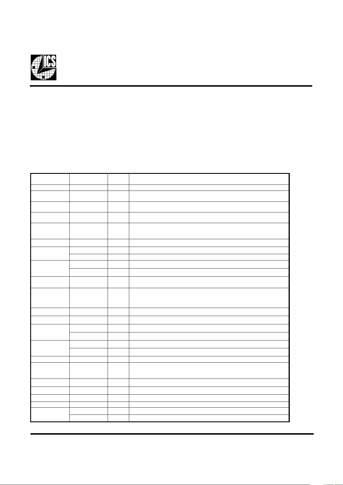
Pin Configuration
NIP
REBMUN
EMANNIPEPYTNOITPIRCSED
11FERTUO.tuptuokcolcecnereferzHM813.41,V3.3
,52,81,01,9,2
54,73,33,23
DDVRWP.ylppusrewopV3.3
31XNI
kcabdeefdna)Fp33(pacdaollanretnisah,tupnilatsyrC
.2Xmorfrotsiser
42XTUO
daollanretnisaH.zHM813.41yllanimon,tuptuolatsyrC
)Fp33(pac
,12,41,6,5
,63,92,82
94,14
DNGRWP.ylppusV3.3rofsnipdnuorG
7,8]0:1[66V3TUO.BUHrofstuptuokcolczHM66dexiFV3.3
11
0KLCICP
1
TUO.SKLCUPCsuonorhcnyShtiw,stuptuokcolcICPV3.3
0SFNI.norewoptadehctaltupnI.tibtcelesycneuqerftupnicigoL
21
1KLCICP
1
TUO.SKLCUPCsuonorhcnyShtiw,stuptuokcolcICPV3.3
1SFNI.norewoptadehctaltupnI.tibtcelesycneuqerftupnicigoL
,61,71,91,02
31,51
]2:7[KLCICPTUO.SKLCUPCsuonorhcnyShtiw,stuptuokcolcICPV3.3
22#DPNI
otniecivedehtnwodrewopotdesuniptupniwolevitcasuonorhcnysA
dnaOCVehtdnadelbasideraskcolclanretniehT.etatsrewopwola
ebtonlliwnwodrewopehtfoycnetalehT.deppotseralatsyrceht
.sm3nahtretaerg
32KLCSNIIfotupnikcolC
2
.tupniC
42ATADSO/IIrofnipataD
2
.tnarelotV5yrtiucricC
43
zHM84TUO.BSUroftuptuokcolczHM84dexiFV3.3
3SFNI.norewoptadehctaltupnI.tibtcelesycneuqerftupnicigoL
53
2SFNI.norewoptadehctaltupnI.tibtcelesycneuqerftupnicigoL
zHM42TUO.tuptuozHM42dexifV3.3
83F_MARDSTUOIybdetceffatonMARDSzHM001gninnureerfV3.3
2
.C
,13,03,72,62
,34,24,04,93
84,74,64,44
]0:11[MARDSTUO
ffodenrutebnacstuptuoMARDSllA.zHM001gninnurtuptuoV3.3
Ihguorht
2
.C
05LDNGRWP.CIPA&UPCrofylppusrewopV5.2rofdnuorG
25,15]0:1[KLCUPCTUO.snipSFmorfdeviredycneuqerftuptuO.tuptuokcolcsubtsoHV5.2
55,35LDDVRWP.CIPAOI,UPCrofylppyusrewopV5.2
45CIPAOITUO.zHM76.61tagninnurstuptuokcolcV5.2
65
4SFNI.norewoptadehctaltupnI.tibtcelesycneuqerftupnicigoL
0FER
1
TUO.tuptuokcolcecnereferzHM813.41,V3.3
The ICS9250-23 is a single chip clock solution for desktop designs using the 810/810E style chipset. It provides all necessary
clock signals for such a system.
Spread spectrum may be enabled through I
2
C programming. Spread spectrum typically reduces system EMI by 8dB to
10dB. This simplifies EMI qualification without resorting to board design iterations or costly shielding. The ICS9250-23
employs a proprietary closed loop design, which tightly controls the percentage of spreading over process and temperature
variations.
Serial programming I
2
C interface allows changing functions, stop clock programming and frequency selection.
Page 3
3
ICS9250-23
Third party brands and names are the property of their respective owners.
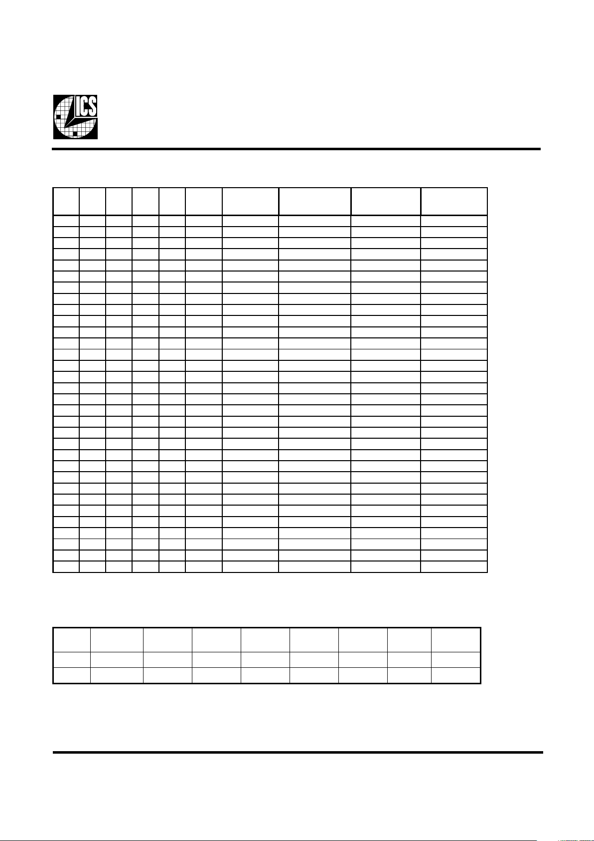
Frequency Selection
Clock Enable Configuration
4SF3SF2SF1SF0SF
UPC
zHM
MARDS
zHM
zHM66V3
ICP
zHM
zHMCIPAOI
00000 00.9605.30100.9605.4352.71
0000 1 00.0700.50100.0700.5305.71
00010 00.1705.60100.1705.5357.71
00011 09.6653.00109.6654.3337.61
00100 00.2700.80100.2700.6300.81
00101 00.5705.21100.5705.7357.81
00110 06.6709.41106.6704.8302.91
00111 00.5805.72100.5805.2452.12
01000 00.8600.20100.8600.4300.71
01001 00.4700.11100.4700.7305.81
01010 00.04100.04100.0700.5305.71
01011 33.33133.33176.6633.3376.61
01100 00.05100.05100.5705.7357.81
01101 00.55100.55105.7757.8383.91
01110 00.66100.66100.3805.1457.22
01111 00.66100.66100.11108.5509.72
10000 77.11177.11125.4762.7336.81
1000 1 87.40187.40168.9639.4364.71
100 10 15.90115.90110.3705.6352.81
100 1 1 09.00109.00172.7636.3328.61
10 100 00.71100.71105.8752.9336.91
10 10 1 57.32157.32105.2852.1426.02
10 1 10 33.33133.33198.8844.4422.22
10111 05.24105.24100.5905.7457.32
11000 00.63152.20105.8652.4331.71
11001 00.04100.50100.0700.5305.71
11010 00.34105.70100.2700.6300.81
11011 09.33186.00154.7637.3368.61
11100 76.64100.01133.3776.6333.81
11101 33.94100.21176.4733.7376.81
11110 03.35192.51142.7726.8303.91
11111 76.66123.52143.3876.1438.02
#DPKLCUPCMARDSCIPAOIzHM66KLCICP
,FER
zHM84
csOsOCV
0WOLWOLWOLWOLWOLWOLFFOFFO
1NONONONONONONONO
Page 4
4
ICS9250-23
Third party brands and names are the property of their respective owners.
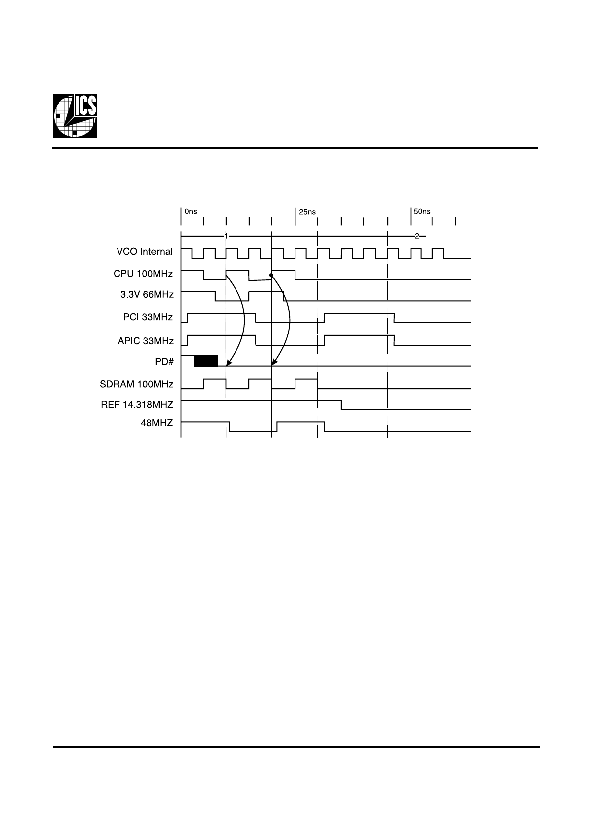
Power Down Waveform
Note
1. After PD# is sampled active (Low) for 2 consective rising edges of CPUCLKs, all
the output clocks are driven Low on their next High to Low tranistiion.
2. Power-up latency <3ms.
3. Waveform shown for 100MHz
Page 5
5
ICS9250-23
Third party brands and names are the property of their respective owners.
Fig. 1
Via to
VDD
Clock trace to load
Series Term. Res.
Programming
Header
Via to Gnd
Device
Pad
2K W
8.2K W
Shared Pin Operation Input/Output Pins
The I/O pins designated by (input/output) serve as dual
signal functions to the device. During initial power-up, they
act as input pins. The logic level (voltage) that is present on
these pins at this time is read and stored into a 5-bit internal
data latch. At the end of Power-On reset, (see AC
characteristics for timing values), the device changes the
mode of operations for these pins to an output function. In
this mode the pins produce the specified buffered clocks to
external loads.
To program (load) the internal configuration register for these
pins, a resistor is connected to either the VDD (logic 1) power
supply or the GND (logic 0) voltage potential. A 10 Kilohm
(10K) resistor is used both to provide the solid CMOS
programming voltage needed during the power-up
programming period and to provide an insignificant load on
the output clock during the subsequent operating period.
Figure 1 shows a means of implementing this function when
a switch or 2 pin header is used. When no jumper is installed
the pin will be pulled high. With the jumper in place the pin
will be pulled low. If programmability is not necessary, then
only a single resistor is necessary. The programming resistors
should be located close to the series termination resistor to
minimize the current loop area. It is more important to locate
the series termination resistor close to the driver than the
programming resistor.
Page 6

6
ICS9250-23
Third party brands and names are the property of their respective owners.
1. The ICS clock generator is a slave/receiver, I2C component. It can read back the data stored in the latches for
verification. Read-Back will support Intel PIIX4 "Block-Read" protocol.
2. The data transfer rate supported by this clock generator is 100K bits/sec or less (standard mode)
3. The input is operating at 3.3V logic levels.
4. The data byte format is 8 bit bytes.
5. To simplify the clock generator I
2
C interface, the protocol is set to use only "Block-Writes" from the controller. The
bytes must be accessed in sequential order from lowest to highest byte with the ability to stop after any complete byte
has been transferred. The Command code and Byte count shown above must be sent, but the data is ignored for those
two bytes. The data is loaded until a Stop sequence is issued.
6. At power-on, all registers are set to a default condition, as shown.
General I2C serial interface information
The information in this section assumes familiarity with I2C programming.
For more information, contact ICS for an I
2
C programming application note.
How to Write:
• Controller (host) sends a start bit.
• Controller (host) sends the write address D2
(H)
• ICS clock will acknowledge
• Controller (host) sends a dummy command code
• ICS clock will acknowledge
• Controller (host) sends a dummy byte count
• ICS clock will acknowledge
• Controller (host) starts sending first byte (Byte 0)
through byte 5
• ICS clock will acknowledge each byte one at a time.
• Controller (host) sends a Stop bit
How to Read:
• Controller (host) will send start bit.
• Controller (host) sends the read address D3
(H)
• ICS clock will acknowledge
• ICS clock will send the byte count
• Controller (host) acknowledges
• ICS clock sends first byte (Byte 0) through byte 5
• Controller (host) will need to acknowledge each byte
• Controller (host) will send a stop bit
Notes:
Controller (Host) ICS (Slave/Receiver)
Start Bit
Address
D3
(H)
A
CK
Byte Count
ACK
Byte 0
ACK
Byte 1
ACK
Byte 2
ACK
Byte 3
ACK
Byte 4
ACK
Byte 5
ACK
Stop Bit
How to Read:
Controller (Host) ICS (Slave/Receiver)
Start Bit
Address
D2
(H)
A
CK
Dummy Command Code
A
CK
Dummy Byte Count
A
CK
Byte 0
A
CK
Byte 1
ACK
Byte 2
A
CK
Byte 3
A
CK
Byte 4
A
CK
Byte 5
A
CK
Stop Bit
How to Write:
Page 7

7
ICS9250-23
Third party brands and names are the property of their respective owners.
Byte 0: Functionality and frequency select register (Default=0)
(1 = enable, 0 = disable)
Notes:
1.
Default at power-up will be for latched logic inputs to define frequency, as diplayed by Bit 3.
tiB
noitpircseD
DWP
tiB
)4:7,2(
)4:7,2(tiB
KLCUPC
zHM
MARDS
zHM
66V3
zHM
KLCICP
CIPAOI
zHM
00100
1etoN
00000 00.9605.30100.9605.4352.71
00001 00.0700.50100.0700.5305.71
00010 00.1705.60100.1705.5357.71
00011 09.6653.00109.6654.3337.61
00100 00.2700.80100.2700.6300.81
00101 00.5705.21100.5705.7357.81
00110 06.6709.41106.6704.8302.91
00111 00.5805.72100.5805.2452.12
01000 00.8600.20100.8600.4300.71
01001 00.4700.11100.4700.7305.81
01010 00.04100.04100.0700.5305.71
01011 33.33133.33176.6633.3376.61
01100 00.05100.05100.5705.7357.81
01101 00.55100.55105.7757.8383.91
01110 00.66100.66100.3805.1457.22
01111 00.66100.66100.11108.5509.72
10000 77.11177.11125.4762.7336.81
1000 1 87.40187.40168.9639.4364.71
10010 15.90115.90110.3705.6352.81
10011 09.00109.00172.7636.3328.61
10 100 00.71100.71105.8752.9336.91
10 10 1 57.32157.32105.2852.1426.02
10 110 33.33133.33198.8844.4422.22
10 111 05.24105.24100.5905.7457.32
11000 00.63152.20105.8652.4331.71
11001 00.04100.50100.0700.5305.71
11010 00.34105.70100.2700.6300.81
11011 09.33186.00154.7637.3368.61
11100 76.64100.01133.3776.6333.81
11101 33.94100.21176.4733.7376.81
11110 03.35192.51142.7726.8303.91
11111 76.66123.52143.3876.1438.02
3tiB
stupnidehctal,tceleserawdrahybdetcelessiycneuqerF-0
4:6,2tiBybdetcelessiycneuqerF-1
0
1tiB
lamroN-0
daerpSretneC%52.0±elbanemurtcepsdaerpS-1
1
0tiB
gninnuR-0
stuptuollaetatsirT-1
0
Page 8

8
ICS9250-23
Third party brands and names are the property of their respective owners.
Byte 1: Control Register
(1 = enable, 0 = disable)
Notes:
1. Inactive means outputs are held LOW and are disabled from switching. These outputs are designed to be
configured at power-on and are not expected to be configured during the normal modes of operation.
2. PWD = Power on Default
tiB#niPDWPnoitpircseD
7tiB-0 #3SF
6tiB-0 #0SF
5tiB-0 #2SF
4tiB531 zHM42
3tiB-1 )devreseR(
2tiB431 zHM84
1tiB-1 )devreseR(
0tiB831 F_MARDS
tiB#niPDWPnoitpircseD
7tiB021 7KLCICP
6tiB911 6KLCICP
5tiB711 5KLCICP
4tiB611 4KLCICP
3tiB511 3KLCICP
2tiB31
1
2KLCICP
1tiB211 1KLCICP
0tiB111 0KLCICP
Byte 3: Control Register
(1 = enable, 0 = disable)
Byte 2: Control Register
(1 = enable, 0 = disable)
tiB#niPDWPnoitpircseD
7tiB931 7MARDS
6tiB041 6MARDS
5tiB241 5MARDS
4tiB341 4MARDS
3tiB441 3MARDS
2tiB64
1
2MARDS
1tiB741 1MARDS
0tiB841 0MARDS
tiB#niPDWPnoitpircseD
7tiB-1 )devreseR(
6tiB71 0_66V3
5tiB81 1_66V3
4tiB-0 #4SF
3tiB451 CIPAOI
2tiB-0 #1SF
1tiB151 1KLCUPC
0tiB251 0KLCUPC
Byte 4: Control Register
(1 = enable, 0 = disable)
tiB#niPDWPnoitpircseD
7tiB-1 )devreseR(
6tiB-1 )devreseR(
5tiB-1 )devreseR(
4tiB-1 )devreseR(
3tiB621 11MARDS
2tiB721 01MARDS
1tiB031 9MARDS
0tiB131 8MARDS
Byte 5: Control Register
(1 = enable, 0 = disable)
Page 9

9
ICS9250-23
Third party brands and names are the property of their respective owners.
Absolute Maximum Ratings
Stresses above those listed under Absolute Maximum Ratings may cause permanent damage to the device. These ratings are
stress specifications only and functional operation of the device at these or any other conditions above those listed in the
operational sections of the specifications is not implied. Exposure to absolute maximum rating conditions for extended periods
may affect product reliability.
Group Timing Relationship Table
Core Supply Voltage . . . . . . . . . . . . . . . . . . . . . . . 4.6 V
I/O Supply Voltage . . . . . . . . . . . . . . . . . . . . . . . . . 3.6V
Logic Inputs . . . . . . . . . . . . . . . . . . . . . . . . . . . . . . GND –0.5 V to V
DD
+0.5 V
Ambient Operating Temperature . . . . . . . . . . . . . 0°C to +70°C
Storage Temperature . . . . . . . . . . . . . . . . . . . . . . . –65°C to +150°C
Case Temperature . . . . . . . . . . . . . . . . . . . . . . . . . . 115°C
puorG
zHM66UPCzHM001UPCzHM331UPC
tesffOecnareloTtesffOecnareloTtesffOecnareloT
MARDSotUPCsn5.2sp005sn0.5sp005sn0.0sp005
66V3otUPCsn5.7sp005sn0.5sp005sn0.0sp005
66V3otMARDSsn0.0sp005sn0.0sp005sn0.0sp005
ICPot66V3sn5.3-5.1sp005sn5.3-5.1sp005sn5.3-5.1sp005
TOD&BSUhcnysAA/NhcnysAA/NhcnysAA/N
Electrical Characteristics - Input/Supply/Common Output Parameters
TA = 0 - 70º C; Supply Voltage VDD = 3.3 V +/-5%, V
DDL
= 2.5 V +/-5% (unless otherwise stated)
PARAMETER
S
YMBOL
CO
NDITION
S
MIN TYP MAX UNIT
S
Input High Voltage V
IH
2V
DD
+0.3 V
Input Low Voltage V
IL
VSS-0.3 0.8 V
Input High Current I
IH
VIN = V
DD
-5 5
µ
A
Input Low Current I
IL1
VIN = 0 V; Inputs with no pull-up resistors -5
µ
A
Input Low Current I
IL2
VIN = 0 V; Inputs with pull-up resistors -200
µ
A
Operating I
DD3.3V
Cl = 0 pF; Select @ 66M 119
280
Supply Current I
DDL2.5V
Cl = 0 pF; Select @ 66M 3
25
Power Down Current I
DD3.3VPD
Cl = 0 pF; With Input to Vdd or Gnd
600
µ
A
Input frequency F
i
VDD = 3.3 V 14.318 MHz
Input Capacitance
1
C
IN
Logic Inputs 5 pF
C
INX
X1 & X2 pins 27 45 pF
Transition Time
1
T
Trans
To 1st crossing of target Freq. 3 ms
Settling Time
1
T
S
From 1st crossing to 1% target Freq. 1 3 ms
Clk Stabilization
1
T
Stab
From VDD = 3.3 V to 1% target Freq. 3 ms
T
PZH,TPZL
output enable delay(all outputs) 1 10 ns
T
PHZ,TPLZ
output disable delay(all outputs) 1 10 ns
1
Guaranteed by design, not 100% tested in production.
mA
Delay
1
Page 10

10
ICS9250-23
Third party brands and names are the property of their respective owners.
Electrical Characteristics - CPUCLK
TA = 0 - 70º C; VDD = 3.3 V +/-5%, V
DDL
= 2.5 V +/-5%;
C
L
= 20 pF (unles
s
PARAMETER
S
YMBOL
CO
NDITION
S
Output High Voltage V
OH2B
IOH = -1 mA
Output Low Voltage V
OL2B
IOL = 1 mA
VOH
@MIN
= 1 V
V
OH@MAX
= 2.375V
VOL
@MIN
= 1.2 V
V
OL@MAX
=0.3V
Rise Time t
r2B
1
VOL = 1 V, VOH = 2.0 V
Fall Time t
f2B
1
VOH = 2.0 V, VOL = 0.4 V
Duty Cycle d
t2B
1
VT = 1.25 V
Skew
t
sk2B
1
VT = 1.25 V
Jitter
, Cycle-to-Cycle
t
jcyc-cyc2B
1
VT = 1.25 V (CPU 133, SDRAM 100
Jitter
, Cycle-to-Cycle
t
jcyc-cyc
1
VT = 1.25 V (all other select B)
1
Guaranteed by design, not 100% tested in production.
Output High Current
I
OH2B
Output Low Current
I
OL2B
Electrical Characteristics - IOAPIC
TA = 0 - 70º C; VDD = 3.3 V +/-5%, V
DDL
= 2.5 V +/-5%;
C
L
= 20 pF (unless otherwise state
d)
PARAMETER SYMBOL CONDITIONS MIN TYP MAX UNITS
Output High Voltage V
OH4B
IOH = -18 mA 2.4 2.9 V
Output Low Voltage V
OL4B
IOL = 9 mA 0.25 0.4 V
Output High Current
I
OH4B
VOH = 2.0 V -58 -22
mA
VOL
@MIN
= 1.0 V
31 34.1
V
OL@MAX
=0.2V
7.85 31
Rise Time
1
T
r4B
VOL = 0.4 V, VOH = 2.0 V 0.4 1.28 2 ns
Fall Time
1
T
f4B
VOH = 2.0 V, VOL = 0.4 V 0.4 1.2 1.6 ns
Duty Cycle
1
D
t4B
VT = 1.25 V 45 49.6 55 %
Jitter,
Cycle-to-Cycle
t
jcyc-cyc4B
1
VT = 1.25 V
432 750 ps
1
Guaranteed by design, not 100% tested in production.
mAOutput Low Current
I
OL4B
Page 11

11
ICS9250-23
Third party brands and names are the property of their respective owners.
Electrical Characteristics - PCICLK
TA = 0 - 70º C; VDD = 3.3 V +/-5%, V
DDL
= 2.5 V +/-5%;
C
L
= 60 pF for PCI0 & PCI1, CL = 30 pF for other PCIs
PARAMETER SYMBOL CONDITIONS MIN TYP MAX UNITS
Output High Voltage V
OH1
IOH = -1 mA 2.4 3.25 V
Output Low Voltage V
OL1
IOL = 1 mA 0.03 0.55 V
VOH
@
MIN
= 1 V -71 -33
V
OH@MAX
= 3.135V
-33 -10
VOL
@MIN
= 1.95 V
38 74
V
OL@MAX
=0.4V
22 30
Rise Time
1
t
r1
VOL = 0.4 V, VOH = 2.4 V 0.5 1.65 2
ns
Fall Time
1
t
f1
VOH = 2.4 V, VOL = 0.4 V 0.5 1.53 2 ns
Duty Cycle
1
d
t1
VT = 1.5 V 45 51.1 55 %
Skew
1
t
sk1
VT = 1.5 V 331 500 ps
Jitter
, Cycle-to-Cycle
t
jcyc-cyc1
VT = 1.5 V
185 500 ps
1
Guaranteed by design, not 100% tested in production.
mA
mAOutput High Current
I
OH1
Output Low Current
I
OL1
Electrical Characteristics - 3V66
TA = 0 - 70º C; VDD = 3.3 V +/-5%, V
DDL
= 2.5 V +/-5%;
C
L
= 10 - 30 pF
PARAMETER SYMBOL CONDITIONS
Output High Voltage V
OH1
IOH = -1 mA
Output Low Voltage V
OL1
IOL = 1 mA
VOH
@
MIN
= 1 V
V
OH@MAX
= 3.135V
VOL
@MIN
= 1.95 V
V
OL@MAX
=0.4V
Fall Time
1
t
f1
VOH = 2.4 V, VOL = 0.4 V
Duty Cycle
1
d
t1
VT = 1.5 V
Skew
1
t
sk1
VT = 1.5 V
Jitter
1
,Cycle-to-Cycle
t
jcyc-cyc1
VT = 1.5 V
1
Guaranteed by design, not 100% tested in production.
V
OL
= 0.4 V, VOH = 2.4 V
Rise Time
1
t
r1
I
OH1
I
OL1
Output High Current
Output Low Current
Page 12

12
ICS9250-23
Third party brands and names are the property of their respective owners.
Electrical Characteristics - 24MHz
TA = 0 - 70º C; VDD = 3.3 V +/-5%, V
DDL
= 2.5 V +/-5%; CL = 20 pF (unl
e
PARAM ETER SYMBOL CONDITIONS
Output High Voltage V
OH5
IOH = -1 mA
Output Low Voltage V
OL5
IOL = 1 mA
VOH
@MIN
= 1 V
V
OH@MAX
= 3.135V
VOL
@MIN
= 1.95 V
V
OL@MAX
=0.4V
Rise Time
1
t
r5
VOL = 0.4 V, VOH = 2.4 V
Fall Time
1
t
f5
VOH = 2.4 V, VOL = 0.4 V
Duty Cycle
1
d
t5
VT = 1.5 V
Jitter
1
,Cy cle -to -Cy cle
t
jcyc-cyc5
VT = 1.5 V, 24MHz
1
Guaranteed by design, not 100% tested in production.
Output High Current I
OH5
Output Low Current I
OL5
Electrical Characteristics - 48MHz, REF
TA = 0 - 70º C; VDD = 3.3 V +/-5%, V
DDL
= 2.5 V +/-5%;
C
L
= 20 pF (unles
s
PARAMETER SYMBOL CONDITIONS
Output High Voltage V
OH5
IOH = -1 mA
Output Low Voltage V
OL5
IOL = 1 mA
VOH
@
MIN
= 1 V
V
OH@MAX
= 3.135V
VOL
@MIN
= 1.95 V
V
OL@MAX
=0.4V
Rise Time
1
t
r5
VOL = 0.4 V, VOH = 2.4 V
Fall Time
1
t
f5
VOH = 2.4 V, VOL = 0.4 V
Duty Cycle
1
d
t5
VT = 1.5 V
Jitter
1
, Cycle-to-Cycle
t
jcy
c-cyc5
VT = 1.5 V, 24MHz
Jitter
1
, Cycle-to-Cycle
t
jcy
c-cyc5
VT = 1.5 V, 48MHz
Jitter
1
, Cycle-to-Cycle
t
jcyc-cyc5
VT = 1.5 V, REF
1
Guaranteed by design, not 100% tested in production.
Output High Current
Output Low Current
I
OH5
I
OL5
Page 13

13
ICS9250-23
Third party brands and names are the property of their respective owners.
Electrical Characteristics - SDRAM
TA = 0 - 70º C; VDD = 3.3 V +/-5%, V
DDL
= 2.5 V +/-5%;
C
L
=30 pF
PARAMETER SYMBOL CONDITIONS MIN TYP MAX UNITS
Output High Voltage V
OH1
IOH = -1 mA 2.4 3.28 V
Output Low Voltage V
OL1
IOL = 1 mA 0.03 0.4 V
VOH
@
MIN
= 2 V -85 -54
V
OH@MAX
= 3.135V
-46 -12
VOL
@MIN
= 1 V
54 63
V
OL@MAX
=0.4V
27 53
Rise Time
1
t
r1
VOL = 0.4 V, VOH = 2.4 V 0.4 1.25 1.6 ns
Fall Time
1
t
f1
VOH = 2.4 V, VOL = 0.4 V 0.4 1.53 1.6 ns
Duty Cycle
1
d
t1
VT = 1.5 V 45 53.2 55 %
Skew t
sk1
VT = 1.5 V 267 380 ps
Jitter
1
, Cycle-to-Cycle
t
jcyc-cyc1
VT = 1.5 V
176 250 ps
1
Guaranteed by design, not 100% tested in production.
mA
mA
Output High Current
I
OH1
Output Low Current
I
OL1
(No Sk
ew Window is needed for Group Skew spec.
)
TA = 0 - 70º C; VDD = 3.3 V +/-5%, V
DDL
= 2.5 V +/-5%
24MHz, 48MHz, REF, CPU & IOAPIC load = 20 pF; PCI, SDRAM & 3V66 load = 30 pF.
Refer to Group Offset Waveform diagram for definition of transition edges.
Group Skews (CPU = 66 MHz; SDRAM = 100MHz)
PARAMETER SYMBOL CONDITIONS MIN TYP MAX UNITS
CPU to SDRAM Skew
1
T
sk1 CPU-SDRAM
CPU @ 1.25 V, SDRAM @ 1.5 V 2.0 3.0 ns
CPU to 3V66 Skew
1
T
sk1 CPU-3V66
CPU @ 1.25 V, 3V66 @ 1.5 V 7 8 ns
SDRAM to 3V66 Skew
1
T
sk1 SDRAM-3V66
SDRAM @1.5V, 3V66 @ 1.5 V -500 394 500 ps
3V66 to PCI Skew
1
T
sk1 3V66-PCI
3V66 @1.5V, PCI @ 1.5 V 1.5 2.58 3.5 ns
Group Skews (CPU = 100 MHz; SDRAM = 100MHz)
PARAMETER SYMBOL CONDITIONS MIN TYP MAX UNITS
CPU to SDRAM Skew
1
T
sk1 CPU-SDRAM
CPU @ 1.25 V, SDRAM @ 1.5 V 4.5 5.5 ns
CPU to 3V66 Skew
1
T
sk1 CPU-3V66
CPU @ 1.25 V, 3V66 @ 1.5 V 4.5 4.63 5.5 ns
SDRAM to 3V66 Skew
1
T
sk1 SDRAM-3V66
SDRAM @1.5V, 3V66 @ 1.5 V -500 396 500 ps
3V66 to PCI Skew
1
T
sk1 3V66-PCI
3V66 @1.5V, PCI @ 1.5 V 1.5 2.58 3.5 ns
Group Skews (CPU = 133 MHz; SDRAM = 100MHz)
PARAMETER SYMBOL CONDITIONS MIN TYP MAX UNITS
CPU to SDRAM Skew
1
T
sk1 CPU-SDRAM
CPU @ 1.25 V, SDRAM @ 1.5 V -500 -322 500 ps
CPU to 3V66 Skew
1
T
sk1 CPU-3V66
CPU @ 1.25 V, 3V66 @ 1.5 V -500 -284 500 ps
SDRAM to 3V66 Skew
1
T
sk1 SDRAM-3V66
SDRAM @1.5V, 3V66 @ 1.5 V -500 389 500 ps
3V66 to PCI Skew
1
T
sk1 3V66-PCI
3V66 @1.5V, PCI @ 1.5 V 1.5 2.61 3.5 ns
Page 14

14
ICS9250-23
Third party brands and names are the property of their respective owners.
Group Offset Waveforms
CPU/ITP/HCLK [66MHz (2.5V)]
CPU/ITP/HCLK [100MHz (2.5V)]
SDRAM [11:0, F] & DCLKWR [100MHz (3.3V)]
3V66 Link (ICH / MGCH) [66MHz (3.3V)]
PCI [7:0] LPC/SIO [33MHz (3.3V)]
Ref Clock [14.318MHz (3.3V)]
USB [48MHz (3.3V)]
APIC (CPU/MCH) [16.67MHz (2.5V)]
0ns
CPU 66 Period
CPU 100 Period
SDRAM 100 Period
3V66-PCI
25ns 50ns 75ns
Page 15

15
ICS9250-23
Third party brands and names are the property of their respective owners.
Ordering Information
ICS9250yF-23
Pattern Number (2 or 3 digit number for parts with ROM code patterns)
Package Type
F=SSOP
Revision Designator
Device Type
Prefix
ICS, AV = Standard Device
Example:
ICS XXXX y F - PPP
ICS reserves the right to make changes in the device data identified in
this publication without further notice. ICS advises its customers to
obtain the latest version of all device data to verify that any
information being relied upon by the customer is current and accurate.
INDEX
AREA
INDEX
AREA
12
1 2
N
D
h x 45°
h x 45°
E1
E
SEATING
PLANE
SEATING
PLANE
A1
A
e
-C-
- C -
b
.10 (.004) C
.10 (.004) C
c
L
300 mil SSOP Package
MIN
MAX
MIN
MAXA2.41
2.80.09
5.
110A10.20
0.40.008.016b0.20
0.34.008.0135
c
0.13
0.25.005.010DE
10.03
10.68.395.420E17.40
7.60.291.299eh
0.38
0.64.015.025L0.50
1.02.020.040
Nα0°8°0°8°MIN
MAX
MIN
MAX5618.31
18.55.720.730
10-0034
SYMBOL
In Millimeters In Inches
COMMON DIMENSIONS COMMON DIMENSIONS
SEE VARIATIONS SEE VARIATIONS
0.635 BASIC 0.025 BASIC
Reference Doc.: JEDEC Publication 95, MO-118
VARIATIONS
SEE VARIATIONS SEE VARIATIONS
N
D mm. D (inch)
 Loading...