

Page 1
Integrated
Circuit
Systems, Inc.
General Description Features
ICS9250-13
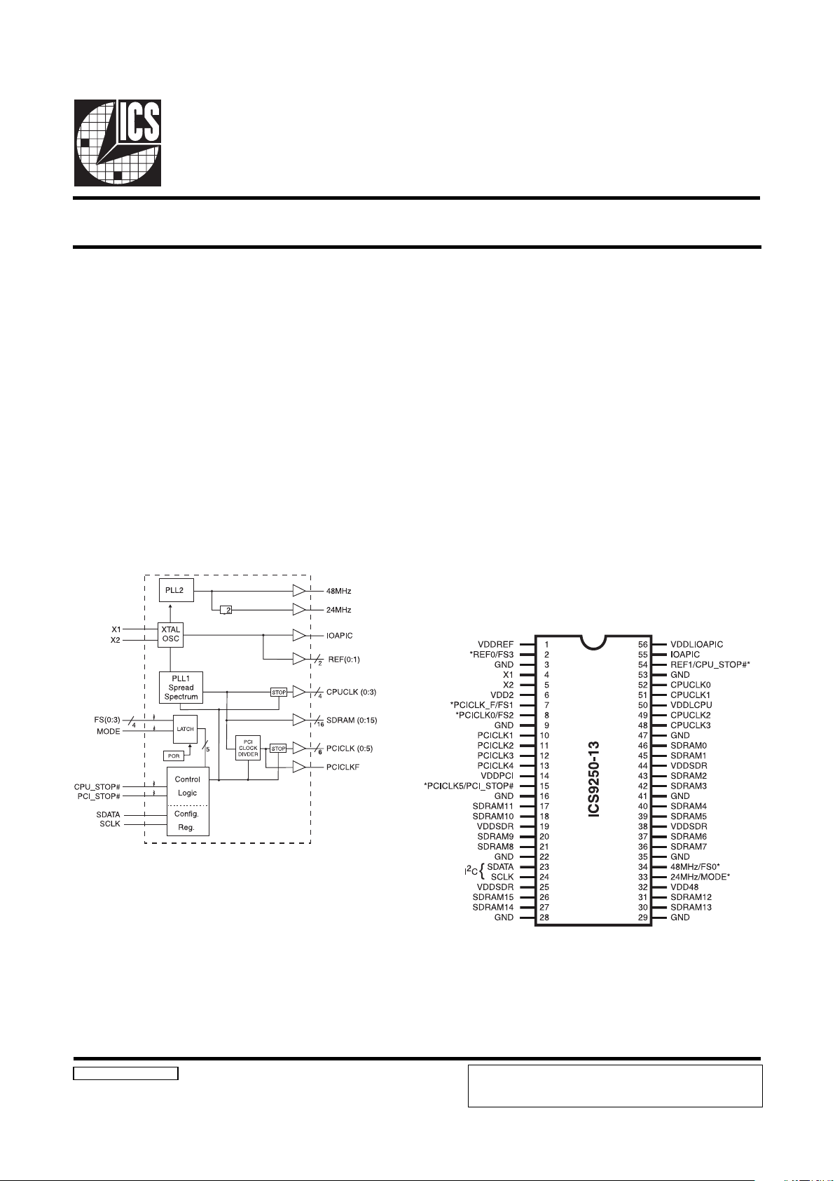
Block Diagram
Pentium is a trademark of Intel Corporation
I2C is a trademark of Philips Corporation
Frequency Generator & Integrated Buffers for PENTIUM/Pro
TM
9250-13 Rev A 3/25/99
Pin Configuration
3.3V outputs: SDRAM, PCI, REF, 48/24MHz
2.5V or 3.3V outputs: CPU
20 ohm CPU clock output impedance
20 ohm PCI clock output impedance
Skew from CPU (earlier) to PCI clock - 1 to 4 ns,
center 2.6 ns.
No external load cap for CL=18pF crystals
±250 ps CPU, PCI clock skew
400ps (cycle to cycle) CPU jitter
Smooth frequency switch, with selections from
50 to 83.3 MHz CPU.
I2C interface for programming
2ms power up clock stable time
Clock duty cycle 45-55%.
56 pin 300 mil SSOP package
3.3V operation, 5V tolerant input.
56-Pin SSOP
Power Groups
VDDREF = REF (0:1), X1, X2
VDDPCI = PCICLK_F, PCICLK(0:5)
VDDSDR = SDRAM (0:11), supply for PLL core,
VDD48 = 24MHz, 48MHz
VDDLIOAPIC = IOAPIC
VDDL2CPU = CPUCLK (0:3)
* Internal Pull-up Resistor of
120K to VDD on indicated inputs
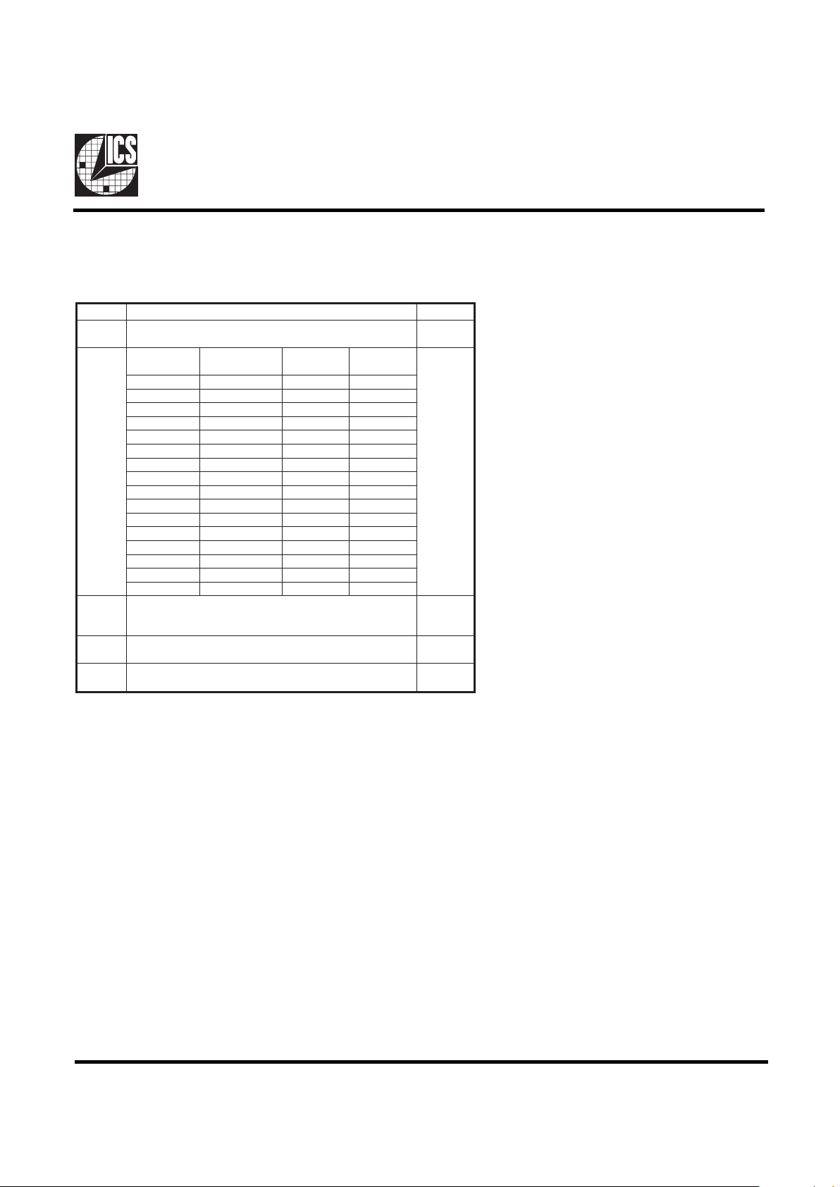
The ICS9250-13 generates all clocks required for high speed
RISC or CISC microprocessor systems such as Intel PentiumPro
or Cyrix. Eight different reference frequency multiplying factors
are externally selectable with smooth frequency transitions.
Spread spectrum may be enabled through I2C programming.
Spread spectrum typically reduces system EMI by 8dB to
10dB. This simplifies EMI qualification without resorting to
board design iterations or costly shielding. The ICS9250-13
employs a proprietary closed loop design, which tightly
controls the percentage of spreading over process and
temperature variations.
Recomended Application:
440LX/EX type chipset Motherboard single chip
clock solution.
ICS reserves the right to make changes in the device data identified in
this publication without further notice. ICS advises its customers to
obtain the latest version of all device data to verify that any
information being relied upon by the customer is current and accurate.
Page 2
2
ICS9250-13
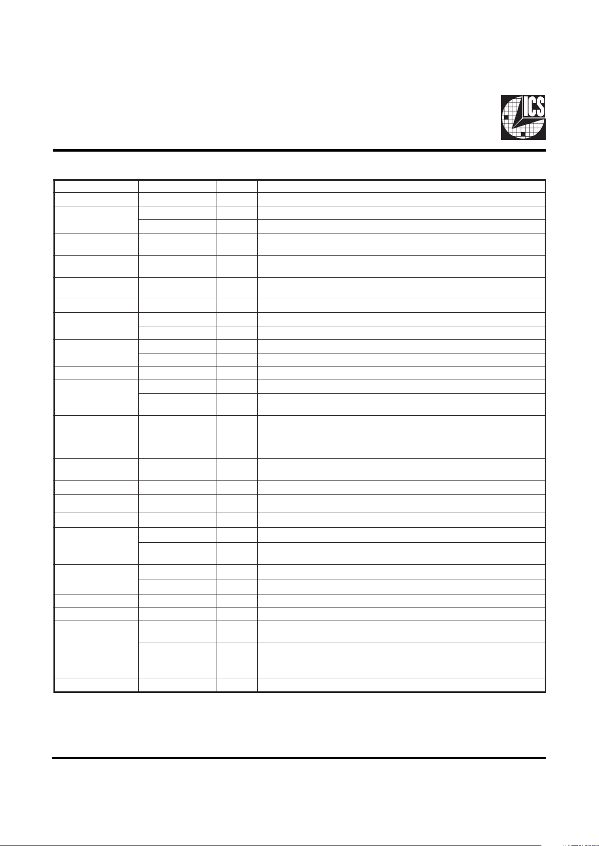
Pin Descriptions
Notes:
1: Internal Pull-up Resistor of 240K to 3.3V on indicated inputs
2: Bidirectional input/output pins, input logic levels are latched at internal power-on-reset. Use 10Kohm resistor to
program logic Hi to VDD or GND for logic low.
REBMUNNIPEMANNIPEPYTNOITPIRCSED
1FERDDVRWPV3.3lanimon,ylppusrewopLATX,)1:0(feR
2
0FERTUO.kcolcecnereferzHM813.41
3SF
2,1
NItupnIdehctaL.niptcelesycneuqerF
,53,92,82,22,61,9,3
35,74,14
DNGRWPdnuorG
41XNI
kcabdeefdna)Fp33(pacdaollanretnisah,tupnilatsyrC
2Xmorfrotsiser
52XTUO
daollanretnisaH.zHM813.41yllanimon,tuptuolatsyrC
)Fp33(pac
41,6ICPDDVRWPV3.3lanimon,)5:0(KLCICPdnaF_KLCICProfylppuS
7
F_KLCICPTUOkcolcICPgninnureerF
1SF
2,1
NItupnIdehctaL.niptcelesycneuqerF
8
0KLCICPTUO.tuptuokcolcICP
2SF
2,1
NItupnIdehctaL.niptcelesycneuqerF
31,21,11,01)4:1(KLCICPTUO.stuptuokcolcICP
51
5KLCICPTUO)1=EDOM,edompotksednI(.tuptuokcolcICP
#POTS_ICP
1
NI
woltupninehw,level0cigoltaskcolc)5:0(KLCICPstlaH
)0=EDOM,edomelibomnI(
,62,12,02,81,71
,73,63,13,03,72
,54,34,24,04,93
64
)51:0(MARDSTUO.stuptuokcolcMARDS
44,83,52,91RDSDDVRWP
,skcolczHM42dnaeroCLLP,)51:0(MARDSrofylppuS
.V3.3lanimon
32ATADSNIroftupniataDI
2
.tupnilairesC
42KLCSNIfotupnikcolCI
2
tupniC
2384DDVRWPlanimonV3.3skcolczHM84rofylppuS
33
zHM42TUOkcolctuptuozHM42
EDOM
2,1
NI
,edoMpotkseD=1,niptcelesnoitcnuf45nip,51niP
.tupnIdehctaL.edoMeliboM=0
43
zHM84TUOkcolctuptuozHM84
0SF
2,1
NItupnIdehctaL.niptcelesycneuqerF
25,15,94,84)3:0(KLCUPCTUOwoL=#POTS_UPCfiwoL.2LDDVybderewop,stuptuokcolcUPC
05UPCLDDVRWPlanimonV3.3roV5.2rehtie,)3:0(UPCrofylppuS
45
1FERTUO
tuptuoFERsihT)1=EDOM,edoMpotkseDni(,kcolcecnereferzHM813.41
.sdaolSUBASIrofreffubREGNORTSehtsi
#POTS_UPC
1
NI
eliboMni(woltupninehw,level0cigoltaskcolc)3:0(KLCUPCstlaH
)0=EDOM,edoM
55CIPAOITUOCIPAOI.1LDDVybderewoPzHM813.41.tuptuokcolc
65CIPAOILDDVRWPlanimonV3.3ro5.2rehtie,CIPAOIrofylppuS
Page 3
3
ICS9250-13
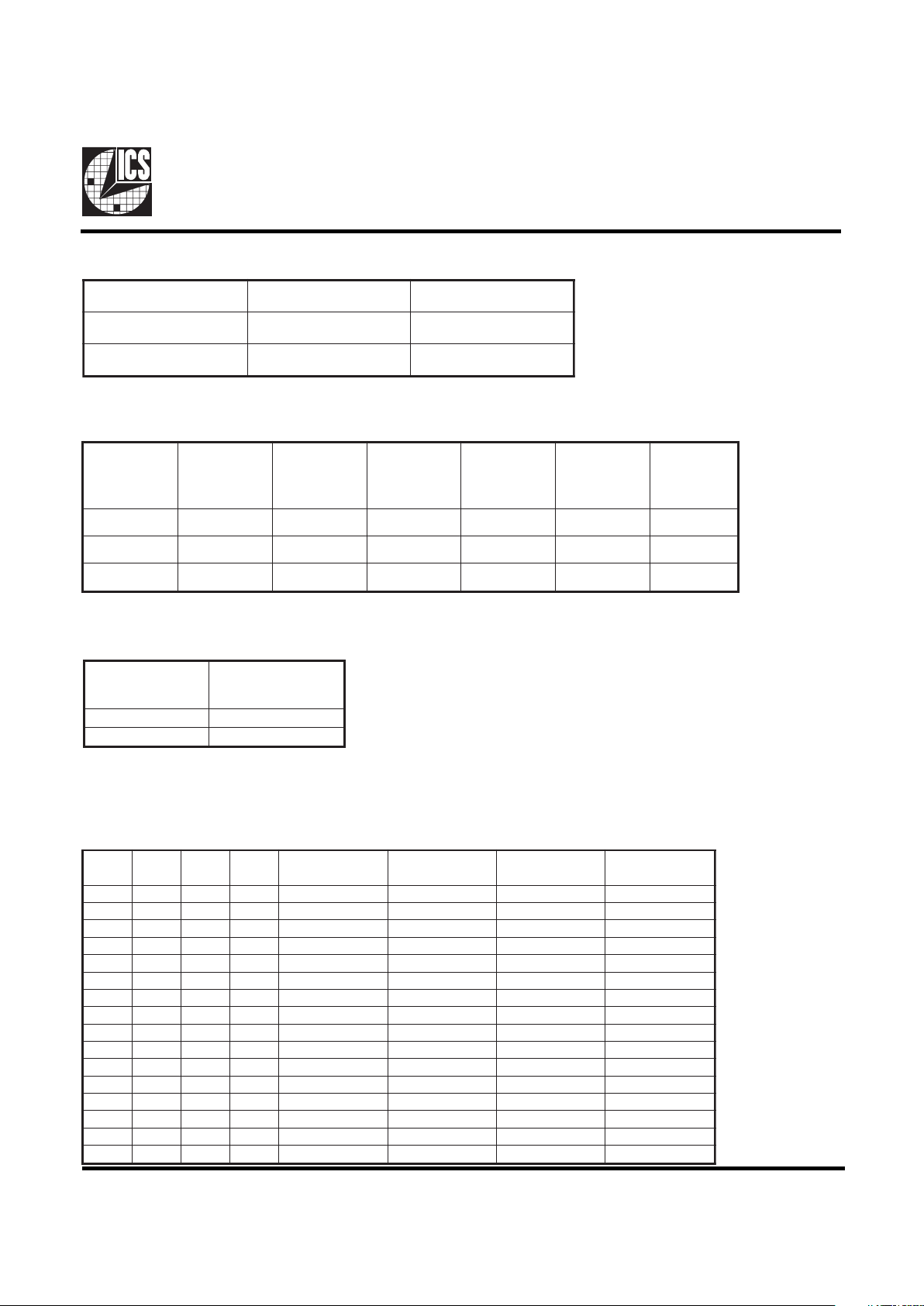
Functionality
VDD1,2,3 = 3.3V±5%, V
DDL
1,2 = 2.5V±5% or 3.3±5%, TA=0 to 70°C
Crystal (X1, X2) = 14.31818MHz
5.2_#3.3UPC
leveltupnI
)ataDdehctaL(
rofdetceleSreffuB
:tanoitarepo
1DDVV5.2
0DDVV3.3
CPU 3.3#_2.5V Buffer selector for CPUCLK and IOAPIC drivers.
Power Management Functionality
Mode Pin - Power Management Input Control
52niP,EDOM
)tupnIdehctaL(
64niP51niP
0
#POTS_UPC
)TUPNI(
#POTS_ICP
)TUPNI(
1
1FER
)TUPTUO(
5KLCICP
)TUPTUO(
#POTS_UPC#POTS_ICP
KLCUPC
stuptuO
KLCICP
)5:0(
,F_KLCICP
,FER
zHM84/42
MARDSdna
latsyrC
CSO
OCV
01 woLdeppotSgninnuRgninnuRgninnuRgninnuR
11 gninnuRgninnuRgninnuRgninnuRgninnuR
10 gninnuRwoLdeppotSgninnuRgninnuRgninnuR
3SF2SF1SF0SF
UPC
)zHM(
MARDS
)zHM(
KLCICP
)zHM(
CIPAOI,FER
)zHM(
0000 00.0900.0900.54813.41
0001 10.9810.9815.44813.41
0010 00.8800.8800.44813.41
0011 99.6899.6805.34813.41
0100 19.5819.5859.24813.41
0101 10.5810.5815.24813.41
0110 00.4800.4800.24813.41
0111 00.2800.2800.14813.41
1000 10.1810.1800.04813.41
1001 00.0800.0856.14813.41
1010 13.3813.3842.43813.41
1011 94.8694.8642.43813.41
1100 00.8700.8700.93813.41
1101 00.5700.5705.73813.41
1110 99.1799.1799.53813.41
1111 28.6628.6614.33813.41
Page 4
4
ICS9250-13
1. The ICS clock generator is a slave/receiver, I2C component. It can read back the data stored in the latches for verification.
Read-Back will support Intel PIIX4 "Block-Read" protocol.
2. The data transfer rate supported by this clock generator is 100K bits/sec or less (standard mode)
3. The input is operating at 3.3V logic levels.
4. The data byte format is 8 bit bytes.
5. To simplify the clock generator I2C interface, the protocol is set to use only "Block-Writes" from the controller. The
bytes must be accessed in sequential order from lowest to highest byte with the ability to stop after any complete byte
has been transferred. The Command code and Byte count shown above must be sent, but the data is ignored for those
two bytes. The data is loaded until a Stop sequence is issued.
6. At power-on, all registers are set to a default condition, as shown.
General I2C serial interface information
The information in this section assumes familiarity with I2C programming.
For more information, contact ICS for an I2C programming application note.
How to Write:
Controller (host) sends a start bit.
Controller (host) sends the write address D2
(H)
ICS clock will acknowledge
Controller (host) sends a dummy command code
ICS clock will acknowledge
Controller (host) sends a dummy byte count
ICS clock will acknowledge
Controller (host) starts sending first byte (Byte 0)
through byte 5
ICS clock will acknowledge each byte one at a time.
Controller (host) sends a Stop bit
How to Read:
Controller (host) will send start bit.
Controler (host) sends the read address D3
(H)
ICS clock will acknowledge
ICS clock will send the byte count
Controller (host) acknowledges
ICS clock sends first byte (Byte 0) through byte 5
Controller (host) will need to acknowledge each byte
Controller (host) will send a stop bit
Notes:
Controller (Host) ICS (Slave/Receiver)
Start Bit
Address
D3
(H)
AC
K
Byte Count
ACK
Byte
0
ACK
Byte 1
ACK
Byte
2
ACK
Byte
3
ACK
Byte 4
ACK
Byte
5
ACK
Stop Bit
How to Read:
Controller (Host) ICS (Slave/Receiver)
Start Bit
Address
D2
(H)
AC
K
Dummy Command Code
AC
K
Dummy Byte Count
AC
K
Byte 0
AC
K
Byte 1
AC
K
Byte 2
ACK
Byte 3
AC
K
Byte 4
AC
K
Byte 5
AC
K
Stop Bit
How to Write:
Page 5
5
ICS9250-13
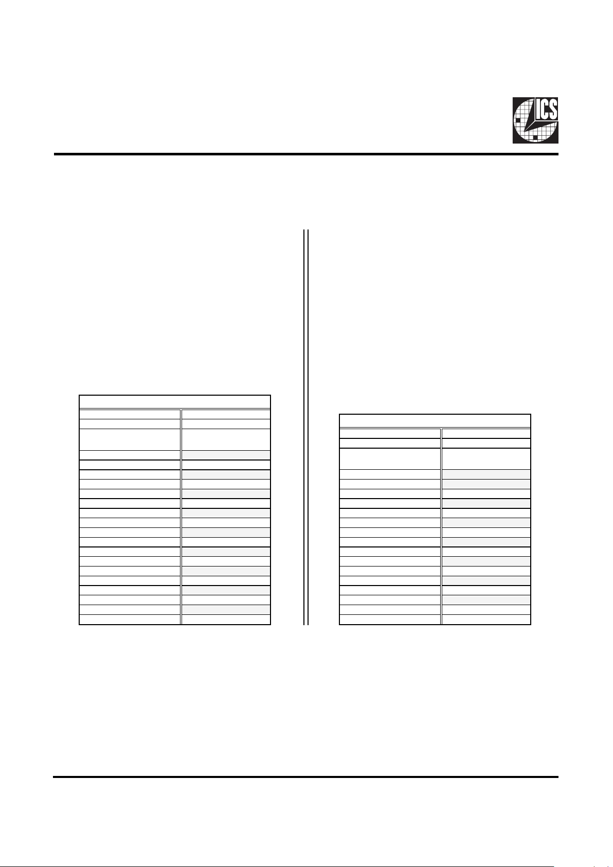
Byte0: Functionality and Frequency Select Register (default = 0)
Serial Configuration Command Bitmap
Note 1. Default at Power-up will be for latched logic inputs to define frequenc,. Bits 2, 6:4 are default to 0000.
tiBnoitpircseDDWP
7tiB
noitaludoMmurtcepSdaerpS%52.0±-0
noitaludoMmurtcepSdaerpS%6.0±-1
1
tiB
)4:6,2(
)4:6,2(tiB
KLCUPC
)zHM(
MARDS
)zHM(
KLCICP
)zHM(
XXX
1etoN
000000.0900.0900.54
100010.9810.9815.44
010000.8800.8800.44
110099.6899.6805.34
001019.5819.5859.24
101010.5810.5815.24
011000.4800.4800.24
111000.2800.2800.14
000110.1810.1815.04
100100.0800.0800.04
010113.3813.3856.14
110194.8694.8642.43
001100.8700.8700.93
101100.5700.5705.73
011199.1799.1799.53
111128.6628.6614.33
3tiB
,tceleserawdrahybdetcelessiycneuqerF-0
stupnidehctal
4:6,2tiBybdetcelessiycneuqerF-1
0
1tiB
noitarepolamroN-0
delbanEmurtcepSdaerpS-1
1
0tiB
gninnuR-0
stuptuollaetatsirT-1
0
Page 6

6
ICS9250-13
Byte 1: Control Register
(1 = enable, 0 = disable)
Notes:
1. Inactive means outputs are held LOW and are disabled
from switching.
tiB#niPDWPnoitpircseD
7tiB-1 )devreseR(
6tiB-1 )devreseR(
5tiB-X#2SF
4tiB-X#0SF
3tiB841 )tcanI/tcA(3KLCUPC
2tiB941 )tcanI/tcA(2KLCUPC
1tiB151 )tcanI/tcA(1KLCUPC
0tiB251 )tcanI/tcA(0KLCUPC
Notes:
1. Inactive means outputs are held LOW and are disabled
from switching.
Byte 2: Control Register
(1 = enable, 0 = disable)
tiB#niPDWPnoitpircseD
7tiB-X#3SF
6tiB71 )tcanI/tcA(F_KLCICP
5tiB511 )tcanI/tcA(5KLCICP
4tiB311 )tcanI/tcA(4KLCICP
3tiB211 )tcanI/tcA(3KLCICP
2tiB111 )tcanI/tcA(2KLCICP
1tiB011 )tcanI/tcA(1KLCICP
0tiB81 )tcanI/tcA(0KLCICP
Byte 3: Control Register
(1 = enable, 0 = disable)
Notes:
1. Inactive means outputs are held LOW and are disabled
from switching.
tiB#niPDWPnoitpircseD
7tiB631 )tcanI/tcA(7MARDS
6tiB731 )tcanI/tcA(6MARDS
5tiB931 )tcanI/tcA(5MARDS
4tiB041 )tcanI/tcA(4MARDS
3tiB241 )tcanI/tcA(3MARDS
2tiB341 )tcanI/tcA(2MARDS
1tiB541 )tcanI/tcA(1MARDS
0tiB641 )tcanI/tcA(0MARDS
Notes:
1. Inactive means outputs are held LOW and are disabled
from switching.
Byte 4: Control Register
(1 = enable, 0 = disable)
tiB#niPDWPnoitpircseD
7tiB621 )tcanI/tcA(51MARDS
6tiB721 )tcanI/tcA(41MARDS
5tiB031 )tcanI/tcA(31MARDS
4tiB131 )tcanI/tcA(21MARDS
3tiB711 )tcanI/tcA(11MARDS
2tiB811 )tcanI/tcA(01MARDS
1tiB021 )tcanI/tcA(9MARDS
0tiB121 )tcanI/tcA(8MARDS
Byte 5: Control Register
(1 = enable, 0 = disable)
Notes:
1. Inactive means outputs are held LOW and are disabled
from switching.
tiB#niPDWPnoitpircseD
7tiB-1 )devreseR(
6tiB-1 )devreseR(
5tiB-1 )devreseR(
4tiB551 )tcanI/tcA(CIPAOI
3tiB-X#1SF
2tiB-1 )devreseR(
1tiB451 )tcanI/tcA(1FER
0tiB21 )tcanI/tcA(0FER
Page 7

7
ICS9250-13
CPU_STOP# Timing Diagram
CPU_STOP# is an asychronous input to the clock synthesizer. It is used to turn off the CPU clocks for low power operation.
CPU_STOP# is synchronized by the ICS9250-13. The minimum that the CPU clock is enabled (CPU_STOP# high pulse) is 100
CPU clocks. All other clocks will continue to run while the CPU clocks are disabled. The CPU clocks will always be stopped in
a low state and start in such a manner that guarantees the high pulse width is a full pulse. CPU clock on latency is less than 4
CPU clocks and CPU clock off latency is less than 4 CPU clocks.
Notes:
1. All timing is referenced to the internal CPU clock.
2. CPU_STOP# is an asynchronous input and metastable conditions may exist. This signal is synchronized
to the CPU clocks inside the ICS9250-13.
3. All other clocks continue to run undisturbed. (including SDRAM outputs).
Page 8

8
ICS9250-13
PCI_STOP# Timing Diagram
PCI_STOP# is an asynchronous input to the ICS9250-13. It is used to turn off the PCICLK (0:5) clocks for low power operation.
PCI_STOP# is synchronized by the ICS9250-13 internally. The minimum that the PCICLK (0:5) clocks are enabled (PCI_STOP#
high pulse) is at least 10 PCICLK (0:5) clocks. PCICLK (0:5) clocks are stopped in a low state and started with a full high pulse
width guaranteed. PCICLK (0:5) clock on latency cycles are only one rising PCICLK clock off latency is one PCICLK clock.
Notes:
1. All timing is referenced to the Internal CPUCLK (defined as inside the ICS9248 device.)
2. PCI_STOP# is an asynchronous input, and metastable conditions may exist. This signal is required to be synchronized
inside the ICS9248.
3. All other clocks continue to run undisturbed.
4. CPU_STOP# is shown in a high (true) state.
Page 9

9
ICS9250-13
Pins 2, 7, 8, 25, and 26 on the ICS9250-13 serve as dual
signal functions to the device. During initial power-up, they
act as input pins. The logic level (voltage) that is present on
these pins at this time is read and stored into a 4-bit internal
data latch. At the end of Power-On reset, (see AC
characteristics for timing values), the device changes the
mode of operations for these pins to an output function. In
this mode the pins produce the specified buffered clocks to
external loads.
To program (load) the internal configuration register for these
pins, a resistor is connected to either the VDD (logic 1)
power supply or the GND (logic 0) voltage potential. A 10
Kilohm(10K) resistor is used to provide both the solid CMOS
programming voltage needed during the power-up
programming period and to provide an insignificant load on
the output clock during the subsequent operating period.
Figs. 1 and 2 show the recommended means of implementing
this function. In Fig. 1 either one of the resistors is loaded
onto the board (selective stuffing) to configure the devices
internal logic. Figs. 2a and b provide a single resistor loading
option where either solder spot tabs or a physical jumper
Shared Pin Operation Input/Output Pins
Fig. 1
header may be used.
These figures illustrate the optimal PCB physical layout
options. These configuration resistors are of such a large
ohmic value that they do not effect the low impedance clock
signals. The layouts have been optimized to provide as little
impedance transition to the clock signal as possible, as it
passes through the programming resistor pad(s).
Page 10

10
ICS9250-13
Fig. 2a
Fig. 2b
Page 11

11
ICS9250-13
Absolute Maximum Ratings
Supply Voltage. . . . . . . . . . . . . . . . . . . . . . . . . . . 7.0 V
Logic Inputs . . . . . . . . . . . . . . . . . . . . . . . . . . . . GND 0.5 V to VDD +0.5 V
Ambient Operating Temperature . . . . . . . . . . . . 0°C to +70°C
Storage Temperature . . . . . . . . . . . . . . . . . . . . . . 65°C to +150°C
Stresses above those listed under Absolute Maximum Ratings may cause permanent damage to the device. These ratings are
stress specifications only and functional operation of the device at these or any other conditions above those listed in the
operational sections of the specifications is not implied. Exposure to absolute maximum rating conditions for extended periods
may affect product reliability.
Electrical Characteristics - Input/Supply/Common Output Parameters
TA = 0 - 70º C; Supply Voltage VDD = 3.3 V +/-5%, V
DDL
= 2.5 V +/-5% (unless otherwise stated)
PARAMETER SYMBOL CONDITIONS MIN TYP MAX UNITS
Operating Supply Current I
DD2.5OP
CL = 0 pF; Select @ 66.8 MHz
20
mA
Skew
1
T
CPU-PCI2VT
=1.5 V; VTL=1.25 V 1 2.15 4 ns
T
CPU-SDRAM2
VT=1.5 V;VTL=1.25 V 70 500 ps
1
Guaranteed by design, not 100% tested in production.
Electrical Characterist ics - Input/ S upply/Common Output Parameters
TA = 0 - 70C; Supply Volta ge VDD = 3.3 V ±5% VDDL = 2.5V ± 5% (unless otherwise stated)
PARAMETER SYMBOL CONDITIONS MIN TYP M AX UNITS
Input High Voltage V
IH
2V
DD
+0.3 V
Input Low V oltage V
IL
VSS-0.3 0.8 V
Inpu t High C urrent I
IH
VIN = V
DD
0.1 5 µA
Input L ow Curr e nt I
IL1
VIN = 0 V; I nputs with no pull-up r e sistor s -5 2.0 µA
Input L ow Curr e nt I
IL2
VIN = 0 V; Inputs w i t h pul l -up res i stors -200 -10 0 µA
Op e rat i ng Supply C urrent I
DD2.5OP
CL = 0 pF; Select @ 66 MHz 160 mA
Inp ut Frequency F
i
VDD = 3.3 V 12 14.32 16 MHz
C
IN
Logic Inputs 5 pF
C
INX
X 1 & X2 pins 27 36 45 pF
Tr a ns ition T ime
1
T
Trans
To 1st crossing of target Freq. 1.3 2 ms
Settling Time
1
T
s
0.3
Clk Stabiliza tion
1
T
STAB
From VDD = 3.3 V to 1% t arget F req. < 2 2 ms
T
CPU-PCI2VT
= 1.5 V 1 2.15 4 ns
T
CPU-SDRAM2VT
= 1.5 V
70 500 ps
1
G ua rant eed by design, not 100% t este d i n produc ti o n.
Input Capacitance
1
Skew
1
Page 12

12
ICS9250-13
Electrical Characteristics - CPUCLK
TA = 0 - 70º C; VDD = 3.3 V +/-5%, V
DDL
= 2.5 V +/-5%; CL = 20 pF (unless otherwise stated)
PARAMETER SYMBOL CONDITIONS MIN TYP MAX UNITS
Output High Voltage V
OH2B
IOH = -8.0 mA 2 2.4 V
Output Low Voltage V
OL2B
IOL = 12 mA 0.32 0.4 V
Output High Current I
OH2B
VOH =1.7 V -37 -16 mA
Output Low Current I
OL2B
VOL = 0.7 V 19 26 mA
Rise Time t
r2B
1
VOL = 0.4 V, VOH = 2.0 V 1.3 1.9 ns
Fall Time t
f2B
1
VOH = 2.0 V, VOL = 0.4 V 1.5 1.9 ns
Duty Cycle d
t2B
1
VT = 1.25 V 45 50 55 %
Skew t
sk2B
1
VT = 1.25 V 78 175 ps
Jitter, Cycle-to-cycle
tj
cyc-cyc2B
1
VT = 1.25 V, Normal or Spread mode 170 350 ps
Jitter, One Sigma t
j
1σ2B
1
VT = 1.25 V 45 150 ps
Jitter, Absolute
t
jabs2B
1
VT = 1.25 V
-250 120 250 ps
1
Guaranteed by design, not 100% tested in production.
Electrical Characteristics - SDRAM
TA = 0 - 70º C; VDD = 3.3 V +/-5%, V
DDL
= 2.5 V +/-5%; CL = 30 pF (unless otherwise stated)
PARAMETER SYMBOL CONDITIONS MIN TYP MAX UNITS
Output High Voltage V
OH3
IOH = -25 mA 2.4 2.85 V
Output Low Voltage V
OL3
IOL = 20 mA 0.35 0.4 V
Output High Current I
OH3
VOH = 2.0 V -60 -40 mA
Output Low Current I
OL3
VOL = 0.8 V 35 45 mA
Rise Time T
r3
1
VOL = 0.4 V, VOH = 2.4 V 1.6 2.4 ns
Fall Time T
f3
1
VOH = 2.4 V, VOL = 0.4 V 1.8 2.2 ns
Duty Cycle D
t3
1
VT = 1.5 V 46 52 56 %
Skew
1
T
sk1
VT = 1.5 V
325 500 ps
1
Guarenteed by design, not 100% tested in production.
Page 13

13
ICS9250-13
Electrical Characteristics - PCICLK
TA = 0 - 70º C; VDD = 3.3 V +/-5%, V
DDL
= 2.5 V +/-5%; CL = 30 pF (unless otherwise stated)
PARAMETER SYMBOL CONDIT IONS MIN TYP MAX UNITS
Output High Voltage V
OH1
IOH = -28 mA 2.4 3 V
Output Low Voltage V
OL1
IOL = 9.4 mA 0.17 0.4 V
Output High Current I
OH1
VOH = 2.0 V -60 -40 mA
Output Low Current I
OL1
VOL = 0.8 V 41 4 5 mA
Rise Time
1
t
r1
VOL = 0.4 V, VOH = 2.4 V 1.4 2 ns
Fall Time
1
t
f1
VOH = 2.4 V, VOL = 0.4 V 1.4 2 ns
Duty Cycle
1
d
t1
VT = 1.5 V 45 50 55 %
Skew
1
t
sk1
VT = 1.5 V 280 500 ps
Jitter, Cycle-to-cycle
1
t
jcy
c-cyc1a
VT = 1.5 V, Normal or Spread mode 230 400 ps
Jitter, One Sigma
1
t
j
1σ1a
VT = 1.5 V 75 150 ps
Jitter, Absolute
1
t
jabs1a
VT = 1.5 V
-250 160 250 ps
1
Guaranteed by design, not 100% tested in production.
Electrical Characteristics - IOAPIC
TA = 0 - 70º C; VDD = 3.3 V +/-5%, V
DDL
= 2.5 V +/-5%; CL = 20 pF (unless otherwise stated)
PARAMETER SYMBOL CONDITIONS MIN TYP MAX UNITS
Output High Voltage V
OH4B
IOH = -8.0 mA 2 2.3 V
Output Low Voltage V
OL4B
IOL = 12 mA 0.3 0.4 V
Output High Current I
OH4B
VOH =1.7 V -26 -15 mA
Output Low Current I
OL4B
VOL = 0.7 V 19 27 mA
Rise Time t
r4B
1
VOL = 0.4 V, VOH = 2.0 V 1.3 2.2 ns
Fall Time t
f4B
1
VOH = 2.0 V, VOL = 0.4 V 1.35 2 ns
Duty Cycle d
t4B
1
VT = 1.25 V 45 52 55 %
Jitter, One Sigma t
j
1σ4B
1
VT = 1.25 V 235 350 ps
Jitter, Absolute
t
jabs4B
1
VT = 1.25 V
-800 510 800 ps
1
Guaranteed by design, not 100% tested in production.
Page 14

14
ICS9250-13
Electrical Characteristics - REF, 24 MHz, 48 MHz
TA = 0 - 70º C; VDD = 3.3 V +/-5%, V
DDL
= 2.5 V +/-5%; CL = 20 pF (unless otherwise stated)
PARAMETER SYMBOL CONDITI ONS MIN TYP MAX UNITS
Output High Vol tage V
OH5
IOH = -12 mA 2.4 2.9 V
Output Low Voltage V
OL5
IOL = 10 mA 0.3 0.4 V
Output High Current I
OH5
VOH = 2.0 V -30 -20 mA
Output Low Current I
OL5
VOL = 0.8 V 16 2 3 mA
Rise Time
1
t
r5
VOL = 0.4 V, VOH = 2.4 V 1.95 4 ns
Fall Time
1
t
f5
VOH = 2.4 V, VOL = 0.4 V 2.1 4 ns
Duty Cycle
1
d
t5
VT = 1.5 V 45 51 55 %
Jitter, One Sigma
1
t
j
1s5
VT = 1.5 V 170 400 ps
Jitter, Absolute
1
t
jabs5
VT = 1.5 V
-800 400 800 ps
1
Guaranteed by design, not 100% tested in production.
Page 15

15
ICS9250-13
SSOP Package
LOBMYS SNOISNEMIDNOMMOC SNOITAIRAV D N
.NIM.MON.XAM.NIM.MON.XAM
A590.101.011.DA027.527.037.65
1A800.210.610.
2A880.090.290.
B800.010.5310.
C500.600.5800.
DsnoitairaVeeS
E292.692.992.
eCSB520.0
H004.604.014.
h010.310.610.
L420.230.040.
NsnoitairaVeeS
∝
°0°5°8
X580.390.001.
Ordering Information
ICS9250yF-13
Pattern Number (2 or 3 digit number for parts with ROM code patterns)
Package Type
F=SSOP
Revision Designator
Device Type (consists of 3 or 4 digit numbers)
Prefix
ICS, AV = Standard Device
Example:
ICS XXXX y F - PPP
ICS reserves the right to make changes in the device data identified in
this publication without further notice. ICS advises its customers to
obtain the latest version of all device data to verify that any
information being relied upon by the customer is current and accurate.
 Loading...