

Page 1
Integrated
Circuit
Systems, Inc.
General Description Features
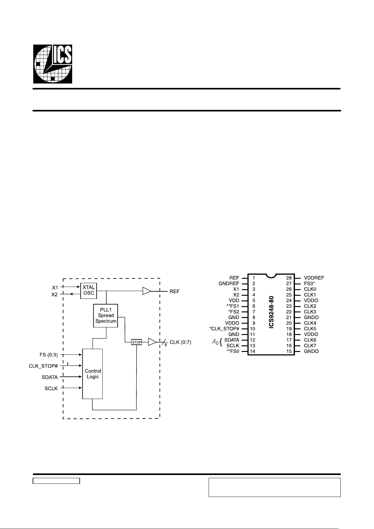
ICS9248-80
Block Diagram
Pentium II is a trademark of Intel Corporation
I2C is a trademark of Philips Corporation
General Purpose 133MHz System Clock
9248-80 Rev A 3/21/00
Pin Configuration
Extended temperature range (-20°C to +70°C)
Output features:
- 8 CLK outputs @ 3.3V, up to 133.34MHz.
- 1-REF output @ 3.3V, 14.31818MHz.
Spread Spectrum for EMI control
I
2
C interface to stop clocks, select spread and frequency.
Excellent power managment feature through CLK_STOP#
and individual stop clocks through I2C.
Input is from a 14.31818MHz crystal.
28-Pin 209 mil SSOP
The ICS9248-80 is a general purpose system clock. It
provides 8 output CLKs, 1 REF CLK and excellent power
management features through CLK_STOP#.
Spread spectrum may be enabled through I2C programming.
Spread spectrum typically reduces EMI by 8dB to 10 dB.
This simplifies EMI qualification without resorting to board
design iterations or costly shielding. The ICS9248-80
employs a proprietary closed loop design, which tightly
controls the percentage of spreading over process and
temperature variations.
* These inputs have a 120K internal pull-up to 3.3V.
** These inputs have a 120K internal pull-down to GND.
ICS reserves the right to make changes in the device data identified in
this publication without further notice. ICS advises its customers to
obtain the latest version of all device data to verify that any
information being relied upon by the customer is current and accurate.
Page 2
2
ICS9248-80
Pin Descriptions
Pin number Pin name Type Description
1 REF OU T 14.318MHz reference clock outputs at 3.3V
2 GNDREF PWR Gnd pin for REF clocks
3 X1 IN XTAL_IN 14 .318 MHz crystal input
4 X2 OUT XTAL_OUT Crystal output
5 VDD PWR
3.3 V power i nput
6, 7, 14, 27 FS (0:3) IN Logic - input for frequency selection
8, 11 GND PWR G round
9, 18, 24 VDDO PWR 3.3V power for CLK outputs
10 CLK_STOP# IN Stops all clock outputs
12 SDATA IN
Data input for I
2
C
serial input.
13 SCLK IN
C
lock input of I
2
C
inp ut
15, 21 GNDO PWR G round for CLK outputs
16, 17, 19, 20 ,
22, 23, 25, 26
CLK (0:7) OU T Clock outputs up to 133.34MHz
28 VDDREF PWR Power pin for REF clocks
3SF2SF1SF0SF
KLC
)zHM(
0000 43.331
0001 10.521
0010 00.021
0011 99.411
0100 99.901
0101 00.501
0110 00.001
0111 00.59
1000 00.09
1001 10.58
1010 00.57
1011 00.07
1100 76.66
1101 00.06
1110 99.45
1111 33.33
Frequency Selection
Page 3
3
ICS9248-80
1. The ICS clock generator is a slave/receiver, I2C component. It can read back the data stored in the latches for verification.
Read-Back will support Intel PIIX4 "Block-Read" protocol.
2. The data transfer rate supported by this clock generator is 100K bits/sec or less (standard mode)
3. The input is operating at 3.3V logic levels.
4. The data byte format is 8 bit bytes.
5. To simplify the clock generator I2C interface, the protocol is set to use only "Block-Writes" from the controller. The
bytes must be accessed in sequential order from lowest to highest byte with the ability to stop after any complete byte
has been transferred. The Command code and Byte count shown above must be sent, but the data is ignored for those
two bytes. The data is loaded until a Stop sequence is issued.
6. At power-on, all registers are set to a default condition, as shown.
General I2C serial interface information
The information in this section assumes familiarity with I2C programming.
For more information, contact ICS for an I2C programming application note.
How to Write:
Controller (host) sends a start bit.
Controller (host) sends the write address D2
(H)
ICS clock will acknowledge
Controller (host) sends a dummy command code
ICS clock will acknowledge
Controller (host) sends a dummy byte count
ICS clock will acknowledge
Controller (host) starts sending first byte (Byte 0)
through byte 5
ICS clock will acknowledge each byte one at a time.
Controller (host) sends a Stop bit
How to Read:
Controller (host) will send start bit.
Controller (host) sends the read address D3
(H)
ICS clock will acknowledge
ICS clock will send the byte count
Controller (host) acknowledges
ICS clock sends first byte (Byte 0) through byte 5
Controller (host) will need to acknowledge each byte
Controller (host) will send a stop bit
Notes:
Controller (Host) ICS (Slave/Receiver)
Start Bit
Address
D3
(H)
ACK
Byte Count
ACK
Byte 0
ACK
Byte 1
ACK
Byte 2
ACK
Byte 3
ACK
Byte 4
ACK
Byte 5
ACK
Stop Bit
H
ow to Read:
Controller (Host) ICS (Slave/Receiver)
Start Bit
Address
D2
(H)
ACK
Dummy Command Code
ACK
Dummy Byte Count
ACK
Byte 0
ACK
Byte 1
ACK
Byte 2
ACK
Byte 3
ACK
Byte 4
ACK
Byte 5
ACK
Stop Bit
H
ow to Write:
Page 4

4
ICS9248-80
Byte 0: Functionality and frequency select register (Default=0)
(1 = Running, 0 = Stopped Low)
Notes:
1. Default is for frequency control thru hardware pins.
tiBnoitpircseDDWP
7tiB
daerpsnwod%5.0-ot0:0
0
daerpsnwod%0.1-ot0:1
)4:6,2(tiB
stiB
ycneuqerfKLC
1etoN
2654
0000 43.331
0001 10.521
0010 00.021
0011 99.411
0100 99.901
0101 00.501
0110 00.001
0111 00.59
1000 00.19
1001 10.58
10 10 00.57
10 11 00.07
1100 76.66
1101 00.06
1110 99.45
1111 33.33
3tiB
)3:0(SFerawdrahybdetcelessiycneuqerF:0
Ifo4:6,2stibybdetcelessiycneuqerf:1
2
C
0
1tiB
lamroN:0
daerpS:1
0
0tiB
gninnurstuptuO:0
detats-irtstuptuO:1
0
Byte 1: CLK output control register
(1 = Running, 0 = Stopped Low)
tiB#niPDWPnoitpircseD
7tiB611 7KLC
6tiB711 6KLC
5tiB911 5KLC
4tiB021 4KLC
3tiB221 3KLC
2tiB321 2KLC
1tiB521 1KLC
0tiB621 0KLC
Page 5

5
ICS9248-80
Absolute Maximum Ratings
Core Supply Voltage . . . . . . . . . . . . . . . . . . . . . . 4.6 V
I/O Supply Voltage . . . . . . . . . . . . . . . . . . . . . . . 3.6V
Logic Inputs . . . . . . . . . . . . . . . . . . . . . . . . . . . . GND 0.5 V to VDD +0.5 V
Ambient Operating Temperature . . . . . . . . . . . . 20°C to +70°C
Storage Temperature . . . . . . . . . . . . . . . . . . . . . . 65°C to +150°C
Stresses above those listed under Absolute Maximum Ratings may cause permanent damage to the device. These ratings are
stress specifications only and functional operation of the device at these or any other conditions above those listed in the
operational sections of the specifications is not implied. Exposure to absolute maximum rating conditions for extended
periods may affect product reliability.
Electrical Charact eristics - Input/Supply/Common Output Parameters
TA = -20°C - +7 0 º C; Supply Voltage VDD = 3.3 V +/-5% (unless otherwise stated)
PARAMETER SYMBOL CONDITIONS MIN TYP MAX UNITS
Input High Voltage V
IH
2V
DD
+0.3 V
Input L ow Voltag e V
I
L
V
S
S
-0.3 0.8 V
Inpu t High Current I
I
H
V
I
N
= V
DD
0.1 5
µ
A
Input Low Current I
IL1
VIN = 0 V; Inputs with no pull-up resis t ors -5 2.0
µ
A
Input Low Current I
IL2
VIN = 0 V; Inputs with pull-up resist ors -2 00 -100
µ
A
Operatin g Supply Current
I
DD2.5OPCL
= 0 pF; Select @ 66 MHz 50 100 mA
Input frequenc y F
i
VDD = 3 .3 V; 14.318 MH z
C
IN
Logic Inputs 5 pF
C
INX
X1 & X2 pins 6 pF
Transition Time
1
T
Trans
To first crossing of target Freq. 1.3 2 ms
Settling Time
1
T
S
From f i rst crossing t o 1% of target Freq. 0.3 ms
Clk Stabilization
1
T
STAB
From VDD = 3.3 V to 1% target Freq.
< 3 3 ms
1
G ua ranteed by d e sign, not 100% t e sted in pr odu c t i on.
Inpu t C a pacitance
1
Page 6

6
ICS9248-80
Ele ctri cal Characteri stics - CLK
TA = -20°C - + 70º C; VDD = 3.3 V +/-5%; CL = 30 p F (unless otherwise st a ted)
PARAMETER SYMBOL CONDITIONS MIN TYP MAX UNITS
Output High Voltage V
OH3
IOH = -1 mA 2 V
Output Low Voltage V
OL3
IOL = 1 mA 0.4 V
O utput High Current I
OH3
V
OH@Min
= 1.0 V,VOH@Max = 2375 V -27 27 mA
Ou tput Low Current I
OL3
V
OL@Min
= 1.2 V, VOL@ M a x = 0.3 V 27 30 mA
Rise Time T
r3
1
VOL = 0.4 V, VOH = 2.0 V 1.33 ns
Fall Time T
f3
1
VOH = 2.0 V, VOL = 0 .4 V 1.4 ns
Duty Cycle D
t3
1
VT = 1.25 V 455558%
Skew
1
T
sk1
VT = 1.25 V
250 ps
Ji tter, cyc-cyc t
jcyc
VT = 1.25 V
250 ps
Jitter, Absolute
1
t
jabs1
VT = 1.25 V
250 ps
1
G ua renteed by d e sign, not 100% t e sted in pr odu c t i on.
Page 7

7
ICS9248-80
ICS reserves the right to make changes in the device data identified in
this publication without further notice. ICS advises its customers to
obtain the latest version of all device data to verify that any
information being relied upon by the customer is current and accurate.
A
2
SEE
DETAIL “A”
E1
c
END VIEW
E
Pin 1
TOP VIEW
Index
Area
PARTING LINE
L
DETAIL “A”
A
1
e
b
A
SIDE VIEW
-C-
D
SEATING
PLANE
.004
C
D/2
E1 /2
BOTTOM VIEW
Country of origin location and ejector pin on
package bottom is optional and depends on
assembly location.
Ordering Information
ICS9248yF-80-T
Designation for tape and reel packaging
Pattern Number (2 or 3 digit number for parts with ROM code patterns)
Package Type
F=SSOP
Revision Designator (will not correlate with datasheet revision)
Device Type (consists of 3 or 4 digit numbers)
Prefix
ICS, AV = Standard Device
Example:
ICS XXXX y F - PPP - T
209 mil SSOP Package
Dimensions in inches
LOBMYS
NOMMOC
SNOISNEMID
SNOITAIRAV
D
.NIM.MON.XAMN .NIM.MON.XAM
A-- 870.041232.0442.0652.0
1A200.0-- 61232.0442.0652.0
2A560.0960.0370.002272.0482.0592.0
b900.0210.0510.042113.0323.0533.0
c400.0-010.082093.0204.0314.0
DsnoitairaVeeS03093.0204.0314.0
1E791.0902.0022.0
eCSB6520.0
E192.0703.0323.0
L220.0030.0730.0
NsnoitairaVeeS
µ
°0 °4 °8
 Loading...