

Page 1
Integrated
Circuit
Systems, Inc.
General Description Features
ICS9248-73
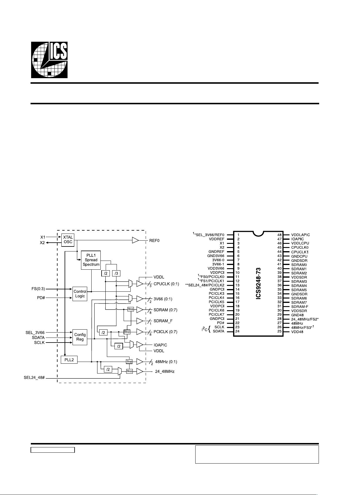
Block Diagram
Pentium II is a trademark of Intel Corporation
I2C is a trademark of Philips Corporation
Frequency Timing Generator for Pentium II Systems
9248-73 Rev B 2/10/00
Pin Configuration
Generates the following system clocks:
- 2 - CPUs @ 2.5V , up to 150MHz.
- 1 - IOAPIC @ 2.5V, PCI/2MHz.
- 9 - SDRAMs @ 3.3V, up to 150MHz.
- 2 - 3V66 @ 3.3V, 2x PCI MHz.
- 8 - PCIs @ 3.3V.
- 2 - 48MHz, @ 3.3V fixed.
- 1 - REF @ 3.3V, 14.318MHz.
- 1 - 24_48MHz, @ 3.3V fixed.
Supports spread spectrum modulation ,
down spread 0 to -0.5%, ±0.25% center spread.
I
2
C support for power management
Efficient power management scheme through PD#
Uses external 14.138 MHz crystal
48-Pin 300 mil SSOP
The ICS9248-73 is a single chip clock for Intel Pentium II.
It provides all necessary clock signals for such a system.
Spread spectrum may be enabled through I2C programming.
Spread spectrum typically reduces EMI by 8dB to 10 dB.
This simplifies EMI qualification without resorting to board
design iterations or costly shielding. The ICS9248-73
employs a proprietary closed loop design, which tightly
controls the percentage of spreading over process and
temperature variations.
Power Groups
GNDREF, VDDREF = REF & Crystal
GND3V66, VDD3V66 = 3V66
GNDPCI, VDDPCI = PCICLK
GNDCOR, VDDCOR = PLL core
GND48, VDD48 = 48MHz
GNDSDR, VDDSDR = SDRAM
GNDLCPU, VDDLCPU = CPUCLK
GNDAPIC, VDDAPIC = IOAPIC
*120K ohm pull-up to VDD on indicated inputs.
**60K ohm pull-up to VDD on indicated inputs.
1. These pins will have 2x drive strength
ICS reserves the right to make changes in the device data identified in
this publication without further notice. ICS advises its customers to
obtain the latest version of all device data to verify that any
information being relied upon by the customer is current and accurate.
Page 2
2
ICS9248-73
Pin Descriptions
NIP
REBMUN
EMANNIPEPYTNOITPIRCSED
1
66V3_LESNI.ycneuqerftuptuo66V3ehtstcelesnipsihT
0FERTUO.tuptuokcolcecnereferzHM813.41,V3.3
,01,9,2
83,03,52,81
DDVRWPylppusrewopV3.3
31XNI
kcabdeefdna)Fp33(pacdaollanretnisah,tupnilatsyrC
2Xmorfrotsiser
42XTUO
.zHM813.41yllanimon,tuptuolatsyrC
)Fp33(pacdaollanretnisaH
,12,41,6,5
,43,24,92
DNGRWPylppusV3.3rofsnipdnuorG
8,7)1:0(66V3TUOzHMICPX2tagninnurBUHrofstuptuokcolcV3.3
11
0KLCICPTUOSKLCUPCsuonorhcnyShtiw,stuptuokcolcICPV3.3
0SFNI.norewoptadehctaltupnI.tibtcelesycneuqerftupnicigoL
21
1KLCICPTUOSKLCUPCsuonorhcnyShtiw,stuptuokcolcICPV3.3
1SFNI.norewoptadehctaltupnI.tibtcelesycneuqerftupnicigoL
31
2KLCICPTUOSKLCUPCsuonorhcnyShtiw,stuptuokcolcICPV3.3
#84_42LESNI.tuptuotcelesottupnicigoL
,71,61,51
02,91
)7:3(KLCICPTUOSKLCUPCsuonorhcnyShtiw,stuptuokcolcICPV3.3
22#DPNI
otniecivedehtnwodrewopotdesuniptupniwolevitcasuonorhcnysA
dnaOCVehtdnadelbasideraskcolclanretniehT.etatsrewopwola
ebtonlliwnwodrewopehtfoycnetalehT.deppotseralatsyrceht
.sm3nahtretaerg
32KLCSNIIfotupnikcolC
2
tupniC
42ATADSNIIroftupniataD
2
.tupnilairesC
62
zHM84TUOBSUroftuptuokcolczHM84dexiFV3.3
3SFNI.norewoptadehctaltupnI.tibtcelesycneuqerftupnicigoL
72zHM84TUOBSUroftuptuokcolczHM84dexiFV3.3
82
zHM84_42TUO.#84_42LESybdellortnoctuptuozHM84ro42
2SFNI.norewoptadehctaltupnI.tibtcelesycneuqerftupnicigoL
9284DNGRWPstuptuozHM84rofdnuorG
13F_MARDSTUOIybdetceffatonMARDSzHM001gninnureerfV3.3
2
C
,73,93,04,14
,23,33,53,63
)7:0(MARDSTUO
ffodenrutebnacstuptuoMARDSllA.zHM001gninnurtuptuoV3.3
Ihguorht
2
C
34LDNGRWPCIPA&UPCrofylppusrewopV5.2rofdnuorG
44,54)1:0(KLCUPCTUO
)3:0(SFnognidnepedzHM051otpu,tuptuokcolcsubtsoHV5.2
.3egaprefeRsnip
74CIPAOITUO.zHM2/ICPtagninnurstuptuokcolcV5.2
64,84LDDVRWPCIPAOI,UPCrofylppyusrewopV5.2
Page 3
3
ICS9248-73
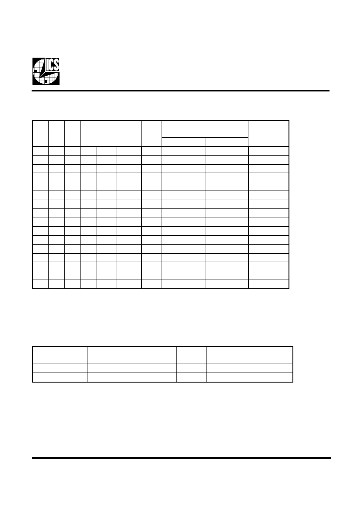
Clock Enable Configuration
#DPKLCUPCMARDSCIPAOIzHM66KLCICP
,FER
zHM84
csOsOCV
0WOLWOLWOLWOLWOLWOLFFOFFO
1NONONONONONONONO
Frequency Selection
3SF2SF1SF0SF
UPC
zHM
MARDS
zHM
ICP
zHM
zHM66V3
zHMCIPAOI
0=66V3_LES1=66V3_LES
0000 32.00132.00114.3328.6628.6607.61
0001 09.00109.00136.3362.7662.7618.61
0010 00.50100.50100.5300.0700.0705.71
0011 98.6633.00144.3398.6698.6627.61
0100 00.02100.02100.04*00.4600.0800.02
0101 00.42100.42133.14*00.4666.2876.02
0110 03.33103.33134.44*00.4668.8812.22
0111 03.33103.33123.3356.6656.6666.61
1000 00.04100.04100.5300.0700.0705.71
100 1 00.05100.05105.73*00.4600.5757.81
10 10 99.41199.41133.83*00.4666.6761.91
10 11 00.0700.50100.5300.0700.0705.71
1100 00.5705.21105.73*00.4600.5757.81
1101 13.3869.42156.14*00.4613.3838.02
1110 00.0900.0900.0300.0600.0600.51
1111 00.5900.5976.1333.3633.3638.51
Note:
* These output frequencies are not synchronous to CPUCLK and do not have spread spectrum modulation.
Page 4
4
ICS9248-73
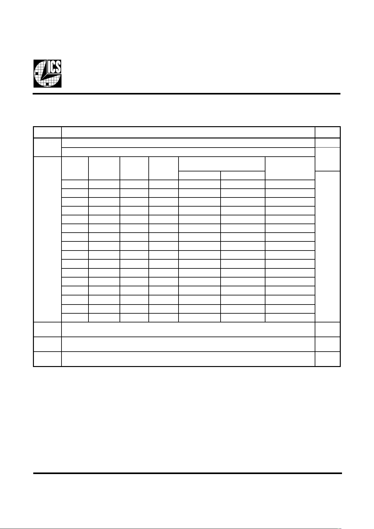
Byte 0: Functionality and frequency select register (Default=0)
(1 = enable, 0 = disable)
tiB
noitpircseD
DWP
7tiB
murtcepSdarepSretneC%52.0±-0
%5.0-ot0murtcepSdaerpSnwoD-1
0
tiB
)4:6,2(
tiB
)4:6,2(
KLCUPC
zHM
MARDS
zHM
KLCICP
zHM
zHM66V3
zHMCIPAOI
0=66V3_LES1=66V3_LES
XXXX
1etoN
000032.00132.00114.3328.6628.6607.61
100009.00109.00136.3362.7662.7618.61
010000.50100.50100.5300.0700.0705.71
110098.6633.00144.3398.6698.6627.61
001000.02100.02100.04*00.4600.0800.02
101000.42100.42133.14*00.4666.2876.02
011003.33103.33134.44*00.4668.8812.22
111003.33103.33123.3356.6656.6666.61
000100.04100.04100.5300.0700.0705.71
100100.05100.05105.73*00.4600.5757.81
010199.41199.41133.83*00.4666.6761.91
110100.0700.50100.5300.0700.0705.71
001100.5705.21105.73*00.4600.5757.81
101113.3869.42156.14*00.4613.3838.02
011100.0900.0900.0300.0600.0600.51
111100.5900.5976.1333.3633.3638.51
3tiB
stupnidehctal,tceleserawdrahybdetcelessiycneuqerF-0
4:6,2tiBybdetcelessiycneuqerF-1
0
1tiB
lamroN-0
elbanemurtcepsdaerpS-1
0
0tiB
gninnuR-0
stuptuollaetatsirT-1
0
Notes:
1. Default at power-up will be for latched logic inputs to define frequency, Bit 2, 6:4 are default to 0000.
* These output frequencies are not synchronous to CPUCLK and do not have spread spectrum modulation.
Page 5

5
ICS9248-73
Byte 1: Control Register
(1 = enable, 0 = disable)
Notes:
1. Inactive means outputs are held LOW and are disabled from switching. These outputs are designed to be configured
at power-on and are not expected to be configured during the normal modes of operation.
2. PWD = Power on Default
tiB#niPDWPnoitpircseD
7tiB-X #3SF
6tiB-X #0SF
5tiB-X #2SF
4tiB821 zHM84-42
3tiB721 zHM84
2tiB621 zHM84
1tiB-0 )devreseR(
0tiB131 F_MARDS
tiB#niPDWPnoitpircseD
7tiB021 7KLCICP
6tiB911 6KLCICP
5tiB711 5KLCICP
4tiB611 4KLCICP
3tiB511 3KLCICP
2tiB31
1
2KLCICP
1tiB211 1KLCICP
0tiB111 0KLCICP
Byte 3: Control Register
(1 = enable, 0 = disable)
Byte 2: Control Register
(1 = enable, 0 = disable)
tiB#niPDWPnoitpircseD
7tiB231 7MARDS
6tiB331 6MARDS
5tiB531 5MARDS
4tiB631 4MARDS
3tiB731 3MARDS
2tiB931 2MARDS
1tiB041 1MARDS
0tiB141 0MARDS
tiB#niPDWPnoitpircseD
7tiB-0 )devreseR(
6tiB71 0_66V3
5tiB81 1_66V3
4tiB-X #66V3_LES
3tiB741 CIPAOI
2tiB-X #1SF
1tiB441 1KLCUPC
0tiB541 0KLCUPC
Byte 4: Control Register
(1 = enable, 0 = disable)
Page 6

6
ICS9248-73
Absolute Maximum Ratings
Core Supply Voltage . . . . . . . . . . . . . . . . . . . . . . 4.6 V
I/O Supply Voltage . . . . . . . . . . . . . . . . . . . . . . . 3.6V
Logic Inputs . . . . . . . . . . . . . . . . . . . . . . . . . . . . GND 0.5 V to VDD +0.5 V
Ambient Operating Temperature . . . . . . . . . . . . 0°C to +70°C
Storage Temperature . . . . . . . . . . . . . . . . . . . . . . 65°C to +150°C
Stresses above those listed under Absolute Maximum Ratings may cause permanent damage to the device. These ratings are
stress specifications only and functional operation of the device at these or any other conditions above those listed in the
operational sections of the specifications is not implied. Exposure to absolute maximum rating conditions for extended
periods may affect product reliability.
Electrical Characteristics - I nput/Supply/Common Out put Parameters
TA = 0 - 70º C; Supply Voltage VDD = 3.3 V +/-5%, V
DDL
= 2.5 V +/- 5% ( u nless otherwise stated)
PARAMETER SYMBOL CONDITIONS MIN TYP MAX UNITS
Input High Voltage V
I
H
2V
DD
+0.3 V
Input L ow Voltag e V
I
L
V
S
S
-0.3 0.8 V
Inpu t High Current I
IH
VIN = V
DD
0.1 5
µ
A
Input Low Current I
IL1
VIN = 0 V; Inputs with no pul l-up resistor s -5 2.0
µ
A
Input Low Current I
I
L2
V
I
N
= 0 V; Inputs with pull-up resis t ors -20 0 -100
µ
A
I
DD3.3OP66
Se l e ct @ 66MHz; Max discret e c ap loads 300
I
DD3.3OP100
Se l e ct @ 100MHz; Ma x discret e cap l o a ds 300
I
DD2.5OP66
Sele c t @ 66MHz; Max discre te cap loads
14 70
I
DD2.5OP100
Se l e ct @ 100MHz; Ma x discret e cap l o a ds
21 100
Power Down
I
DD3.3PDCL
= 0 pF; PWRDWN # = 0
Suppl y C urrent
Input frequenc y F
i
VDD = 3 .3 V 12 14.318 16 MH z
Inpu t C a pacitance
1
C
IN
Logic Inputs 5 pF
C
I
NX
X 1 & X2 pins 27 36 45 pF
Transition Time
1
T
Trans
To 1st cros sing of target Freq. 3 ms
Settling Time
1
T
S
From 1st cr ossing to 1% t a rget Freq. 1 3 ms
Clk Stabilization
1
T
S
tab
From VDD = 3.3 V to 1% ta rget Freq. 3 ms
t
PZH
, t
PZH
O utput enable de l ay (all out put s) 1 10 ns
t
PLZ
, t
PZH
O utput d i a bl e delay (al l out pu ts) 1 10 ns
1
G ua ranteed by d e sign, not 100% t e sted in pr odu c t i on.
Delay
Operating Supply
Current
mA105
mA
mA
380
Page 7

7
ICS9248-73
Ele ctrica l C haracteristics - CPUCLK
TA = 0 - 70º C; VDD = 3.3 V +/-5%, V
DDL
= 2.5 V +/-5%; CL = 20 pF (unless otherwise stated)
PARAMETER SYMBOL CONDITIONS MIN TYP MAX UNITS
Output High Voltage V
OH2B
IOH = -12.0 m A 2 2.36 V
Output Low Voltage V
OL2B
IOL = 12 mA 0.33 0.4 V
O utput High Current I
OH2B
VOH = 1 .7 V -34 -19 mA
Ou tput Low Current I
OL2B
VOL = 0.7 V 19 25 mA
Rise Time t
r2B
1
VOL = 0.4 V, VOH = 2 .0 V 0.4 1.5 2 ns
Fall Time t
f2B
1
VOH = 2.0 V, VOL = 0 .4 V 0.4 1.4 1.8 ns
d
t2B
1
VT = 1.25 V; Freq>= 140MHz 40 48 50 %
V
T
= 1.25 V; Freq< 140MHz 43 48 53 %
Skew t
sk2B
1
VT = 1.25 V 50 175 ps
t
jcyc-cyc2B
1
VT = 1.25 V; CPU @ 66.8 MHz 500
V
T
= 1.25 V; CPU @ 100.23 MHz
130
1
G ua ranteed by d e sign, not 100% t e sted in pr odu c t ion .
250
Duty Cycle
Jitter, Cycle-to-cycle ps
Ele ctri cal Characteri stics - 3V66
TA = 0 - 70º C; VDD = 3.3 V +/-5%, V
DDL
= 2.5 V +/-5%; CL =30 pF
PARAMETER SYMBOL CONDITIONS MIN TYP MAX UNITS
O utput High Voltage V
OH1
IOH = -11 mA 2.4 3.1 V
Output Low Voltage V
OL1
IOL = 9.4 mA 0.18 0.4 V
Ou tput Hig h Current I
OH1
VOH = 2.0 V -55 -22 mA
Output Low Current I
OL1
VOL = 0.8 V 25 43 mA
Rise Time
1
t
r1
VOL = 0.4 V, VOH = 2.4 V 0.5 1.55 2 ns
Fall Time
1
t
f1
VOH = 2.4 V , VOL = 0.4 V 0.5 1.4 2 ns
Duty Cycle
1
d
t1
VT = 1.5 V 45 48 55 %
Skew
1
t
sk1
VT = 1.5 V 50 175 ps
Jitter, Cycle-to-cycle
1
t
jcyc-cyc1
VT = 1.5 V; 3V66 Freq > 75MHz 100 500 ps
Jitter, Cycle-to-cycle
1
t
jcyc-cyc1
VT = 1.5 V; 3V66 Freq < 75MHz
350 500 ps
1
Guar a nt eed by de sign, not 100% tested in product ion.
Page 8

8
ICS9248-73
Electrical Characteristics - IOAPIC
TA = 0 - 70º C; VDD = 3.3 V +/-5%, V
DDL
= 2.5 V +/-5%; CL = 20 pF (unless otherwise st a t e d )
PARAMETER SYMBOL CONDITIONS MIN TYP MAX UNITS
O utput High Voltage V
OH4BIOH
= -8 mA 2 2.3 V
Output Low Voltage V
OL4BIOL
= 12 mA 0.36 0.4 V
Ou tput Hig h Current I
OH4B
VOH = 1.7 V -24 -16 mA
Output Low Current I
OL4B
VOL = 0.7 V 19 23 mA
Rise Time
1
T
r4B
VOL = 0.4 V, VOH = 2.0 V 0.4 1.4 2.1 ns
Fall Time
1
T
f4B
VOH = 2.0 V , VOL = 0.4 V 0 .4 1.45 2.2 ns
Duty Cycle
1
D
t4B
VT = 1.25 V 45 50 55 %
Jitter, Cycle-to-cycle
1
t
jcyc-cyc4BVT
= 1.25 V
140 500 ps
1
Guar a nt eed by de sign, not 100% tested in product ion.
Ele ctri cal Characteri stics - S DRA M
TA = 0 - 70º C; VDD = 3.3 V +/-5%, V
DDL
= 2.5 V +/-5%; CL = 30 pF (unless otherwise st a t e d )
PARAMETER SYMBOL CONDITIONS MIN TYP MAX UNITS
Output High Voltage V
OH3
IOH = -25 mA 2.4 2.9 V
Output Low Voltage V
OL3
IOL = 20 mA 0.32 0.4 V
O utput High Current I
OH3
VOH = 2 .0 V -73 -40 mA
Ou tput Low Current I
OL3
VOL = 0.8 V 41 50 mA
Rise Time T
r3
1
VOL = 0.4 V, VOH = 2 .4 V 0.4 0.95 2 ns
Fall Time T
f3
1
VOH = 2.4 V, VOL = 0 .4 V 0.4 1 2 ns
Duty Cycle D
t3
1
VT = 1.5 V 455355%
Skew
1
T
sk1
VT = 1.5 V 85 250 ps
Jitter, Cycle-to-cycle
t
jcyc-cyc3B
1
VT = 1.25 V
110 250 ps
1
G ua renteed by d e sign, not 100% t e sted in pr odu c t i on.
Page 9

9
ICS9248-73
Ele ctrica l Characteristics - 48MH z/FS3; REF0
TA = 0 - 70º C; VDD = 3.3 V +/-5%, V
DDL
= 2.5 V +/-5%; CL = 20 pF (unless otherwise stated)
PARAMETER SYMBOL CONDITIONS MIN TYP MAX UNITS
O utput High Voltage V
OH5
IOH = -12 mA 2.4 3.1 V
Output Low Voltage V
OL5
IOL = 10 mA 0.19 0.4 V
Ou tput Hig h Current I
OH5
VOH = 2.0 V -55 -22 mA
Output Low Current I
OL5
VOL = 0.8 V 25 42 mA
Rise Time
1
t
r5
VOL = 0.4 V, VOH = 2.4 V 1.1 4 ns
Fall Time
1
t
f5
VOH = 2.4 V, VOL = 0.4 V 1 4 ns
Duty Cycle
1
d
t5
VT = 1.5 V, 48MHz/FS3 45 51 55 %
Duty Cycle
1
d
t5
VT = 1.5 V, REF 45 52 55 %
Jitter, Cycle-to-cycle
1
t
jcyc-cyc5
VT = 1.5 V, 48MHz/F S3 190 500 ps
Jitter, Cycle-to-cycle
1
t
jcyc-cyc5
VT = 1.5 V, RE F
310 1000 ps
1
Guar a nt eed by de sign, not 100% tested in product ion.
Ele ctrical C haracterist ics - 48MHz; 24_48MH z
TA = 0 - 70º C; VDD = 3.3 V +/-5%, V
DDL
= 2.5 V +/-5%; CL = 20 pF (unless otherwise st a t e d )
PARAMETER SYMBOL CONDITIONS MIN TYP MAX UNITS
O utput High Voltage V
OH5
IOH = -12 mA 2.4 2.9 V
Output Low Voltage V
OL5
IOL = 10 mA 0.35 0.4 V
Ou tput Hig h Current I
OH5
VOH = 2.0 V -28 -20 mA
Output Low Current I
OL5
VOL = 0.8 V 16 22 mA
Rise Time
1
t
r5
VOL = 0.4 V, VOH = 2.4 V 1.5 2.4 4 ns
Fall Time
1
t
f5
VOH = 2.4 V , VOL = 0.4 V 1.5 2.2 4 ns
Duty Cycle
1
d
t5
VT = 1.5 V 45 50 55 %
Jitter, Cycle-to-cycle
1
t
jcyc-cyc5
VT = 1.5 V
240 500 ps
1
Guar a nt eed by de sign, not 100% tested in product ion.
Page 10

10
ICS9248-73
Electrical Characteristics - PCICLK
TA = 0 - 70º C; VDD = 3.3 V +/-5%, V
DDL
= 2.5 V +/-5%; CL = 60 pF for PCI0 & PCI1, CL = 30 pF for other PCIs
PARAMETER SYMBOL CONDITIONS MIN TYP MAX UNITS
O utput High Voltage V
OH1
IOH = -11 mA; Pci0 & Pci1 2.4 3.2 V
O utput High Voltage V
OH1
IOH = -11 mA 2.4 3.1 V
Output Low Voltage V
OL1
IOL = 9.4 mA; Pci0 & Pci1 0.12 0.4 V
Output Low Voltage V
OL1
IOL = 9.4 mA 0.2 0.4 V
Ou tput Hig h Current I
OH1
VOH = 2.0 V ; Pci0 & Pci1 -110 -22 mA
Ou tput Hig h Current I
OH1
VOH = 2.0 V -55 -22 mA
Output Low Current I
OL1
VOL = 0.8 V; Pci0 & Pci1 25 82 mA
Output Low Current I
OL1
VOL = 0.8 V 25 42 mA
t
r1
VOL = 0.4 V, VOH = 2.4 V; PCI0:1, CL=60pF 0.5 1.5 2.3 ns
V
OL
= 0.4 V, VOH = 2.4 V; PCI2:7 0.5 1.7 2.3 ns
t
f1
VOH = 2.4 V , VOL = 0.4 V; PCI0:1, CL=60pF 0.5 1.4 2 ns
V
OH
= 2.4 V , VOL = 0.4 V; PCI2:7 0.5 1.7 2 ns
Duty Cycle
1
d
t1
VT = 1.5 V 45 50 55 %
t
sk1
VT = 1.5 V; CL=60pF for Pci0 & PCI1 545 ps
V
T
= 1.5 V; CL=50pF for Pci0 & PCI1 360 50 0 ps
V
T
= 1.5 V; CL=40pF for Pci0 & PCI1 455 ps
Jitter, Cycle-to-cycle
1
t
jcyc-cyc1
VT = 1.5 V
130 500 ps
1
Guar a nt eed by de sign, not 100% tested in product ion.
Skew
1
Fall Time
1
Rise Time
1
Page 11

11
ICS9248-73
Group Offset Waveforms
Group Skews at com m on Transit ion Edges
TA = 0 - 70º C; Supply Voltage VDD = 3.3 V +/-5%, V
DDL
= 2.5 V +/-5% (unless otherwise stated)
CL = 20 pF for CPU and IOAPIC
CL = 50 pF for PCI0 & PCI1, CL = 30 pF for other PCIs, SDRAM and 3V66
GROUP SYMBOL CONDITIONS MIN TYP MAX UNITS
CPU to SDRAM t
CPU-SDRAMVT
= 1.5 V; VTL = 1.25 V
SDRAM leads CPU by 2.5ns for CPU66 0 100 500 ps
CPU leads SDRAM by 5.0ns for CPU100
CPU to 3V66 t
CPU-3V66VT
= 1.5 V; VTL = 1.25 V
CPU leads 3V66 by 7.5ns for CPU66 0 100 500 ps
CPU leads 3V6 6 by 0.0ns for CPU100
IOAPIC to PCI t
IOAP IC-PCI
V T = 1.5 V; VTL = 1.25 V 0 360 500 ps
3V 6 6 to PCI
t
3V66-PCIVT
= 1.5 V
1.5 2.5 4 ns
G uar anteed by design, not 100% tested in production.
Page 12

12
ICS9248-73
Power Down Waveform
Note
1. After PD# is sampled active (Low) for 2 consective rising edges of CPUCLKs, all
the output clocks are driven Low on their next High to Low tranistiion.
2. Power-up latency <3ms.
3. Waveform shown for 100MHz
Page 13

13
ICS9248-73
1. The ICS clock generator is a slave/receiver, I2C component. It can read back the data stored in the latches for verification.
Read-Back will support Intel PIIX4 "Block-Read" protocol.
2. The data transfer rate supported by this clock generator is 100K bits/sec or less (standard mode)
3. The input is operating at 3.3V logic levels.
4. The data byte format is 8 bit bytes.
5. To simplify the clock generator I2C interface, the protocol is set to use only "Block-Writes" from the controller. The
bytes must be accessed in sequential order from lowest to highest byte with the ability to stop after any complete byte
has been transferred. The Command code and Byte count shown above must be sent, but the data is ignored for those
two bytes. The data is loaded until a Stop sequence is issued.
6. At power-on, all registers are set to a default condition, as shown.
General I2C serial interface information
The information in this section assumes familiarity with I2C programming.
For more information, contact ICS for an I2C programming application note.
How to Write:
Controller (host) sends a start bit.
Controller (host) sends the write address D2
(H)
ICS clock will acknowledge
Controller (host) sends a dummy command code
ICS clock will acknowledge
Controller (host) sends a dummy byte count
ICS clock will acknowledge
Controller (host) starts sending first byte (Byte 0)
through byte 5
ICS clock will acknowledge each byte one at a time.
Controller (host) sends a Stop bit
How to Read:
Controller (host) will send start bit.
Controller (host) sends the read address D3
(H)
ICS clock will acknowledge
ICS clock will send the byte count
Controller (host) acknowledges
ICS clock sends first byte (Byte 0) through byte 5
Controller (host) will need to acknowledge each byte
Controller (host) will send a stop bit
Notes:
Controller (Host) ICS (Slave/Receiver)
Start Bit
Address
D3
(H)
ACK
Byte Count
ACK
Byte 0
ACK
Byte 1
ACK
Byte 2
ACK
Byte 3
ACK
Byte 4
ACK
Byte 5
ACK
Stop Bit
How to Read:
Controller (Host) ICS (Slave/Receiver)
Start Bit
Address
D2
(H)
ACK
Dummy Command Code
ACK
Dummy Byte Count
ACK
Byte 0
ACK
Byte 1
ACK
Byte 2
ACK
Byte 3
ACK
Byte 4
ACK
Byte 5
ACK
Stop Bit
How to Write:
Page 14

14
ICS9248-73
Fig. 1
Shared Pin Operation Input/Output Pins
The I/O pins designated by (input/output) on the ICS924873 serve as dual signal functions to the device. During initial
power-up, they act as input pins. The logic level (voltage)
that is present on these pins at this time is read and stored
into a 5-bit internal data latch. At the end of Power-On reset,
(see AC characteristics for timing values), the device changes
the mode of operations for these pins to an output function.
In this mode the pins produce the specified buffered clocks
to external loads.
To program (load) the internal configuration register for these
pins, a resistor is connected to either the VDD (logic 1) power
supply or the GND (logic 0) voltage potential. A 10 Kilohm
(10K) resistor is used to provide both the solid CMOS
programming voltage needed during the power-up
programming period and to provide an insignificant load on
the output clock during the subsequent operating period.
Via to
VDD
Clock trace to load
Series Term. Res.
Programming
Header
Via to Gnd
Device
Pad
2K
8.2K
Figure 1 shows a means of implementing this function when
a switch or 2 pin header is used. With no jumper is installed
the pin will be pulled high. With the jumper in place the pin
will be pulled low. If programmability is not necessary, than
only a single resistor is necessary. The programming resistors
should be located close to the series termination resistor to
minimize the current loop area. It is more important to locate
the series termination resistor close to the driver than the
programming resistor.
Page 15

15
ICS9248-73
ICS reserves the right to make changes in the device data identified in
this publication without further notice. ICS advises its customers to
obtain the latest version of all device data to verify that any
information being relied upon by the customer is current and accurate.
LOBMYSSNOISNEMIDNOMMOCSNOITAIRAVDN
.NIM.MON.XAM.NIM.MON.XAM
A590.201.011.CA026.526.036.84
1A800.210.610.
2A780.090.490.
B800.-5310.
c500.-010.
DsnoitairaVeeS
E192.592.992.
eCSB520.0
H593.-024.
h010.310.610.
L020.-040.
NsnoitairaVeeS
µ
°0- °8
48 Pin 300 mil SSOP Package
“For current dimensional specifications, see JEDEC 95.”
.093
DIA. PIN (Optional)
D/2
E/2
BOTTOM VIEW
A
2
SEE
DETAIL “A”
-E-
c
END VIEW
H
Pin 1
TOP VIEW
Index
Area
PARTING LINE
L
DETAIL “A”
A
1
-e-
B
A
SIDE VIEW
-C-
-D-
SEATING
PLANE
.004
C
Dimensions in inches
Ordering Information
ICS9248yF-73-T
Designation for tape and reel packaging
Pattern Number (2 or 3 digit number for parts with ROM code patterns)
Package Type
F=SSOP
Revision Designator (will not correlate with datasheet revision)
Device Type (consists of 3 or 4 digit numbers)
Prefix
ICS, AV = Standard Device
Example:
ICS XXXX y F - PPP - T
 Loading...