

Page 1
Integrated
Circuit
Systems, Inc.
ICS9248-150
Third party brands and names are the property of their respective owners.
9248-150 Rev B 06/12/01
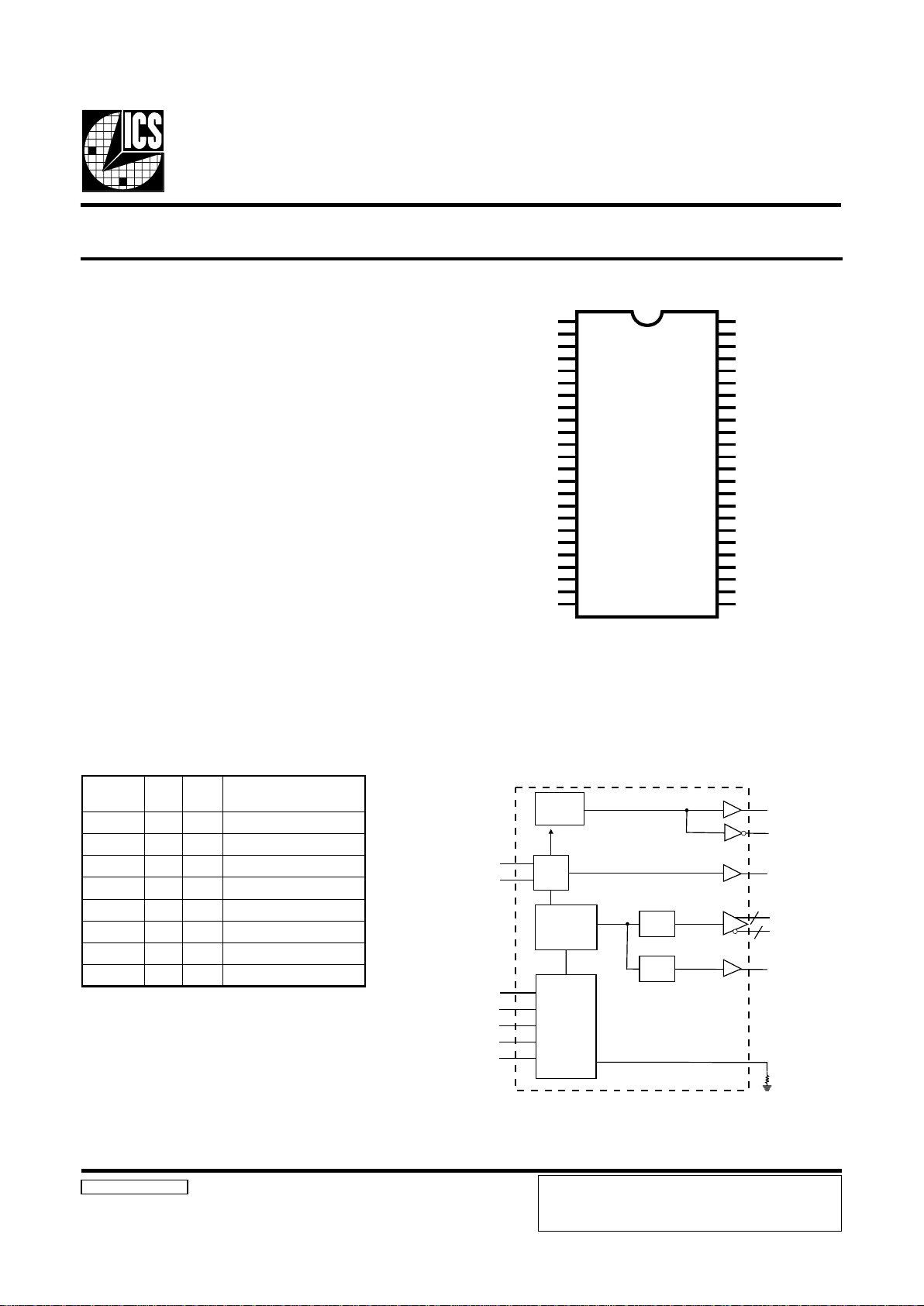
Pin Configuration
48-Pin SSOP and TSSOP
Recommended Application:
ServerWorks Grand Champion Systems.
Output Features:
• 8 - Differential CPU Clock Pairs @ 3.3V
• 1 - 3V 33MHz PCI clocks
• 1 - 48MHz clock
• 1 - Inverted 48MHz clock
• 1 - 14.318 reference output
Features:
• Up to 200MHz frequency support
• Support power management: Power Down Mode
• Supports Spread Spectrum modulation: 0 to -0.5% down
spread.
• Uses external 14.318MHz crystal
• Select logic for Differential Swing Control, Test mode,
Tristate, Power down, Spread Spectrum.
• External resistor for current reference
• FS pins for frequency select
Key Specifications:
• PCI Output jitter <500ps
• CPU Output jitter <200ps
• 48MHz Output jitter <350ps
• REF Output jitter < 1000ps
Frequency Generator for Multi - Processor Servers
Functionality
/331LES
001
0SF1SFnoitcnuF
000 zHM001evitcA
001 edoMtseTzHM001
010 edoMtseTzHM001
011 stuptuollaetatsirT
100 zHM331evitcA
101 edoMtseTzHM331
110 zHM002evitcA
111 devreseR
Block Diagram
PCICLK
VDD48
FS0/48MHz
FS1/48MHz#
GND48
VDDCPU
CPUCLKT0
CPUCLKC0
GNDCPU
CPUCLKT1
CPUCLKC1
VDDCPU
CPUCLKT2
CPUCLKC2
GNDCPU
CPUCLKT3
CPUCLKC3
VDDCPU
REF
SPREAD#
GNDREF
X1
X2
VDDREF
SEL100/133
GNDPCI
VDDA
GNDA
PD#
VDDCPU
CPUCLKT4
CPUCLKC4
GNDCPU
CPUCLKT5
CPUCLKC5
VDDCPU
CPUCLKT6
CPUCLKC6
GNDCPU
CPUCLKT7
CPUCLKC7
VDDCPU
MULTSEL0
MULTSEL1
GND
GNDI REF
I REF
VDDI REF
ICS9248-150
1
2
3
4
5
6
7
8
9
10
11
12
13
14
15
16
17
18
19
20
21
22
23
24
48
47
46
45
44
43
42
41
40
39
38
37
36
35
34
33
32
31
30
29
28
27
26
25
I REF
PLL2
PLL1
Spread
Spectrum
48MHz
PCICLK
48MHz#
X1
X2
XTAL
OSC
CPU
DIVDER
PCI
DIVDER
PD#
SPREAD#
MULTSEL(1:0)
SEL100/133
FS(1:0)
Control
Logic
Config.
Reg.
REF
8
8
CPUCLKT (7:0)
CPUCLKC (7:0)
ICS reserves the right to make changes in the device data
identified in this publication without further notice. ICS advises
its customers to obtain the latest version of all device data to
verify that any information being relied upon by the customer is
Analog Power Groups
VDD48, GND48 = 48MHz, PLL2
VDDA=VDD (core supply voltage 3.3V)
GNDA=Ground for core supply
Digital Power Group
VDDREF , GNDREF = REF, Xtal
Page 2
2
ICS9248-150
Third party brands and names are the property of their respective owners.
General Description
Pin Configuration
The ICS9248-150 is a main clock for ServerWorks Grand Champion Systems.
Spread spectrum typically reduces system EMI by 8dB to 10dB. This simplifies EMI qualification without resorting to
board design iterations or costly shielding. The ICS9248-150 employs a proprietary closed loop design, which tightly
controls the percentage of spreading over process and temperature variations.
REBMUNNIP
EMANNIPEPYTNOITPIRCSED
1KLCICPTUOtuptuokcolcICP
,13,42,81,21,6,2
,34,73
DDVRWPylppusrewopV3.3
3
0SFNIniptcelesycneuqerF
zHM84TUOtuptuokcolczHM84
4
1SFNIniptcelesycneuqerF
#zHM84TUOtuptuokcolczHM84detrevnI
,43,82,12,51,9,5
74,04
DNGRWPylppusV3.3rofsnipdnuorG
,61,24,93,63,33
7,01,31
)0:7(TKLCUPCTUO
tnerruceraesehT.stuptuoUPCriaplaitnereffidfoskcolc"eurT"
.saibegatlovrofderiuqererasrotsiserlanretxednastuptuo
,71,14,83,53,23
8,11,41
)0:7(CKLCUPCTUO
eraesehT.stuptuoUPCriaplaitnereffidfoskcolc"yrotnemelpmoC"
.saibegatlovrofderiuqererasrotsiserlanretxednastuptuotnerruc
91FERTUOzHM813.41tuptuoecnerefeR
02#DAERPSNI
tsohlaitnereffiDehtnoytilanoitcnufmurtcepSdaerpSsekovnI
woLevitcA,skcolc
221XtupnIlatsyrC2XtupnilatsyrCzHM813.41
322XtuptuOlatsyrC1XtuptuolatsyrCzHM813.41
64,52
FERIDDV
,ADDV
RWPV3.3ylppusrewopgolanA
62FERITUO
.sriapKLCUPCehtroftnerrucecnereferehtsehsilbatsenipsihT
otredronidnuorgotdeitrotsisernoisicerpdexifasekatnipsihT
.tnerrucderiuqerehthsilbatse
03,92)0:1(LESTLUMNIstupnitcelesgniwsUPC
44#DPNI.woLevitcA.edomnwod-rewopsekovnI
54,72
FERIDNG
ADNG
RWPylppusV3.3rofsnipdnuorGgolanA
84331/001LESNIzHM331=hgiH,zHM001=woL.tceleSycneuqerFUPC
Page 3
3
ICS9248-150
Third party brands and names are the property of their respective owners.
Truth Table
LES
001/331
0SF1SF
KLCUPC
zHM
KLCICP
ZHM
84
zHM
000 0013384
001 00133elbasiD
010 001elbasiDelbasiD
011 etatsirTetatsirTetatsirT
100 3313384
101 33133elbasiD
110 0023384
111 2/KLCT8/KLCT2/KLCT
CPUCLK Buffer Configuration
snoitidnoCnoitarugifnoCdaoLniMxaM
tuoI
)V03.3(lanimon=ddV
,0MfosnoitanibmocllA
ninwohsrRdna1M
wolebelbat
rofdaoltsetlanimoN
noitarugifnocnevig
%7- I lanimon%7+ I lanimon
tuoI
%5±03.3=ddV
,0MfosnoitanibmocllA
ninwohsrRdna1M
wolebelbat
rofdaoltsetlanimoN
noitarugifnocnevig
%21- I lanimon%21+ I lanimon
Page 4

4
ICS9248-150
Third party brands and names are the property of their respective owners.
0LESTLUM1LESTLUM
tegraTdraoB
ZmreT/ecarT
,RecnerefeR
=ferI
)rR*3(/ddV
tuptuO
tnerruC
,Z@hoV
Am23.2=ferI
00 smho06
%1574=rR
Am23.2=ferI
ferI*5=hoI06@V17.0
00 smho05
%1574=rR
Am23.2=ferI
ferI*5=hoI05@V95.0
01 smho06
%1574=rR
Am23.2=ferI
ferI*6=hoI062/V58.0
01 smho05
%1574=rR
Am23.2=ferI
ferI*6=hoI05@V17.0
10 smho06
%1574=rR
Am23.2=ferI
ferI*4=hoI06@V65.0
10 smho05
%1574=rR
Am23.2=ferI
ferI*4=hoI05@V74.0
11 smho06
%1574=rR
Am23.2=ferI
ferI*7=hoI06@V99.0
11 smho05
%1574=rR
Am23.2=ferI
ferI*7=hoI05@V28.0
00 )viuqeCD(03
%1122=rR
Am5=ferI
ferI*5=hoI03@V57.0
00 )viuqeCD(52
%1122=rR
Am5=ferI
ferI*5=hoI02@V26.0
01 )viuqeCD(03
%1122=rR
Am5=ferI
ferI*6=hoI03@V09.0
01 )viuqeCD(52
%1122=rR
Am5=ferI
ferI*6=hoI02@V57.0
10 )viuqeCD(03
%1122=rR
Am5=ferI
ferI*4=hoI02@06.0
10 )viuqeCD(52
%1122=rR
Am5=ferI
ferI*4=hoI02@V5.0
11 )viuqeCD(03
%1122=rR
Am5=ferI
ferI*7=hoI03@V50.1
11 )viuqeCD(52
%1122=rR
Am5=ferI
ferI*7=hoI02@V48.0
CPUCLK Swing Select Functions
Page 5

5
ICS9248-150
Third party brands and names are the property of their respective owners.
Absolute Maximum Ratings
Supply Voltage . . . . . . . . . . . . . . . . . . . . . . . . . . . . 5.5 V
Logic Inputs . . . . . . . . . . . . . . . . . . . . . . . . . . . . . . GND –0.5 V to V
DD
+0.5 V
Ambient Operating Temperature . . . . . . . . . . . . . 0°C to +70°C
Case Temperature . . . . . . . . . . . . . . . . . . . . . . . . . . 115°C
Storage Temperature . . . . . . . . . . . . . . . . . . . . . . . –65°C to +150°C
Stresses above those listed under Absolute Maximum Ratings may cause permanent damage to the device. These ratings are
stress specifications only and functional operation of the device at these or any other conditions above those listed in the
operational sections of the specifications is not implied. Exposure to absolute maximum rating conditions for extended periods
may affect product reliability.
Electrical Characteristics - Input/Supply/Common Output Parameters
TA = 0 - 70C; Supply Voltage VDD = 3.3 V +/-5%
PARAMETER SYMBOL CONDITIONS MIN TYP MAX UNITS
Input High Voltage V
IH
2V
DD
+0.3 V
Input Low Voltage V
IL
VSS-0.3 0.8 V
Input High Current I
IH
VIN = V
DD
-5 5
µ
A
I
IL1
VIN = 0 V; Inputs with no pull-up resistors -5
µ
A
I
IL2
VIN = 0 V; Inputs with pull-up resistors -200
Operating Supply
Current
I
DD3.3OP
CL = 0 pF; Select @ 100 MHz 181 250
mA
Powerdown Current
I
DD3.3PD
CL = 0 pF; Input address to VDD or GND
52 60
mA
Input Frequency F
i
VDD = 3.3 V 14.318 MHz
Pin Inductance L
p
in
7nH
C
IN
Logic Inputs 5 pF
C
OUT
Output pin capacitance 6 pF
C
INX
X1 & X2 pins 27 45 pF
Transition time
1
T
trans
To 1st crossing of target frequency 3 ms
Settling time
1
T
s
From 1st crossing to 1% target frequency 3 ms
Clk Stabilization
1
T
STAB
From VDD = 3.3 V to 1% target frequency 3 ms
t
PZH,tPZL
Output enable delay (all outputs) 1 10 ns
t
PHZ,tPLZ
Output disable delay (all outputs) 1 10 ns
1
Guaranteed by design, not 100% tested in production.
Delay
1
Input Capacitance
1
Input Low Current
Page 6

6
ICS9248-150
Third party brands and names are the property of their respective owners.
Electrical Characteristics - CPU
TA = 0 - 70C; VDD=3.3V +/-5%; CL = 10-20 pF (unless otherw ise specified)
PA RAMETER SYMBOL CONDITIONS M IN TYP M AX UNITS
Output Impedance R
DSP2B
1
VO = VDD*(0.5) 714
Ω
Output Impedance R
DSN2B
1
VO = VDD*(0.5) 714
Ω
Output High Voltage V
OH2B
IOH = -1 mA 2 V
Output Low Vol tage V
OL2B
IOL = 1 mA 0.4 V
Output High Current
I
OH2B
2
V
OH@MIN
= 1.0 V, V
OH@MAX
= 2.375 V -27 -27
mA
Output Low Current
I
OL2B
2
V
OL @MI N
= 1.2 V, V
OL @MAX
= 0.3 V 27 30
mA
Rise Time t
r2B
1
VOL = 20%, VOH = 80% 175 324 700 ps
Fall Time t
f2B
1
VOH = 80%, VOL = 20% 175 501 700 ps
Diff. Crossover Volta
g
V
x
VDD = 3.3V 45 50 55 %
Duty Cy cle
d
t2B
1
VT = 50% 45 51.2 55
%
Skew CPUT0:7 t
sk2B
1
VT = 50% 83.8 100 p s
Skew CPU C0:7 t
sk2B
1
VT = 50% 78.5 100 p s
Jitter
t
jcyc-cyc
1
VT = 50%
86 150 ps
1
Guaranteed by design, not 100% tested in production.
2
I
OWT
can be varied and is selectable thru the MULTSEL pin.
Electrical Characteristics - REF
TA = 0 - 70C; VDD=3.3V +/-5%; CL = 10-20 pF (unless otherwise specified)
PARAMETER SYMBOL CONDITIONS MIN TYP MAX UNITS
Output Frequency F
O1
MHz
Output Impedance R
DSP1
1
VO = VDD*(0.5) 20 48 60 Ω
Output High Volt age V
OH
1
IOH = -1 mA 2.4 V
Output Low Voltage V
OL
1
IOL = 1 mA 0.4 V
Output High Current
I
OH
1
V
OH@MIN
= 1.0 V, V
OH@MAX
= 3.135 V -29 -23
mA
Output Low Current
I
OL
1
V
OL @MIN
= 1.95 V, V
OL @MAX
= 0.4 V 29 27
mA
Rise Time t
r1
1
VOL = 0.4 V, VOH = 2.4 V 1 1.6 4 ns
Fall Time t
f1
1
VOH = 2.4 V, VOL = 0.4 V 1 2.4 4 ns
Duty Cycle
d
t1
1
VT = 1.5 V 45 53.5 55
%
Skew t
sk1
1
VT = 1.5 V N/A ps
Jitter
t
jcyc-cyc
1
VT = 1.5 V
305 1000 ps
1
Guaranteed by design, not 100% tested in production.
Page 7

7
ICS9248-150
Third party brands and names are the property of their respective owners.
Electrical Characteristics - PCI
TA = 0 - 70C; VDD=3.3V +/-5%; CL = 10-30 pF (unless otherwise specified)
PARAMETER SYMBOL CONDITIONS MIN TYP MAX UNITS
Output Frequency F
O1
MHz
Output Impedance R
DSP1
1
VO = VDD*(0.5) 12 33 55 Ω
Output High Volt age V
OH
1
IOH = -1 mA 2.4 V
Output Low Voltage V
OL
1
IOL = 1 mA 0.55 V
Output High Current
I
OH
1
V
OH@MIN
= 1.0 V, V
OH@MAX
= 3.135 V -33 -33
mA
Output Low Current
I
OL
1
V
OL @MIN
= 1.95 V, V
OL @MAX
= 0.4 V 30 38
mA
Rise Time t
r1
1
VOL = 0.4 V, VOH = 2.4 V 0.5 1.2 2 ns
Fall Time t
f1
1
VOH = 2.4 V, VOL = 0.4 V 0.5 1.2 2 ns
Duty Cycle
d
t1
1
VT = 1.5 V 45 49.9 55
%
Skew t
sk1
1
VT = 1.5 V 500 ps
Jitter
t
jcyc-cyc
1
VT = 1.5 V
139.7 500 ps
1
Guaranteed by design, not 100% tested in production.
Electrical Characteristics - 48MHz
TA = 0 - 70C; VDD=3.3V +/-5%; CL = 10-20 pF (unless otherwise specified)
PARAMETER SYMBOL CONDITIONS MIN TYP MAX UNITS
Output Frequency F
O1
MHz
Output Impedance R
DSP1
1
VO = VDD*(0.5) 20 48 60 Ω
Output High Volt age V
OH
1
IOH = -1 mA 2.4 V
Output Low Voltage V
OL
1
IOL = 1 mA 0.4 V
Output High Current
I
OH
1
V
OH@MIN
= 1.0 V, V
OH@MAX
= 3.135 V -29 -23
mA
Output Low Current
I
OL
1
V
OL @MIN
= 1.95 V, V
OL @MAX
= 0.4 V 29 27
mA
Rise Time t
r1
1
VOL = 0.4 V, VOH = 2.4 V 1 1.3 4 ns
Fall Time t
f1
1
VOH = 2.4 V, VOL = 0.4 V 1 1.6 4 ns
Duty Cycle
d
t1
1
VT = 1.5 V 45 52.5 55
%
Skew t
sk1
1
VT = 1.5 V N/A ps
Jitter
t
jcyc-cyc
1
VT = 1.5 V
175 350 ps
1
Guaranteed by design, not 100% tested in production.
Page 8

8
ICS9248-150
Third party brands and names are the property of their respective owners.
PD# Timing Diagram
The power down selection is used to put the part into a very low power state without turning off the power to the part. PD# is
an asynchronous active low input. This signal needs to be synchronized internal to the device prior to powering down the clock
synthesizer.
Internal clocks are not running after the device is put in power down. When PD# is active low all clocks need to be driven to a
low value and held prior to turning off the VCOs and crystal. The power up latency needs to be less than 3 mS. The power down
latency should be as short as possible but conforming to the sequence requirements shown below.
Notes:
1. As shown, the outputs Stop Low on the next falling edge after PD# goes low.
2. PD# is an asynchronous input and metastable conditions may exist. This signal is synchronized inside this part.
3. The shaded sections on the VCO and the Crystal signals indicate an active clock.
CPUCLKT
CPUCLKC
VCO
Crystal
PD#
Page 9

9
ICS9248-150
Third party brands and names are the property of their respective owners.
Ordering Information
ICS9248yF-150-T
Designation for tape and reel packaging
Pattern Number (2 or 3 digit number for parts with ROM code patterns)
Package Type
F=SSOP
Revision Designator (will not correlate with datasheet revision)
Device Type
Prefix
ICS, AV = Standard Device
Example:
ICS XXXX y F - PPP - T
INDEX
AREA
INDEX
AREA
12
1 2
N
D
h x 45°
h x 45°
E1
E
SEATING
PLANE
SEATING
PLANE
A1
A
e
-C-
- C -
b
.10 (.004) C
.10 (.004) C
c
L
300 mil SSOP Package
MIN
MAX
MIN
MAX
A
2.41
2.80.09
5.
110
A1
0.20
0.40.008.016b0.20
0.34.008.0135
c
0.13
0.25.005.010DE
10.03
10.68.395.420E17.40
7.60.291.299eh
0.38
0.64.015.025L0.50
1.02.020.040
Nα0°8°0°8°MIN
MAX
MIN
MAX4815.75
16.00.620.630
10-0034
SYMBOL
In Millimeters In Inches
COMMON DIMENSIONS COMMON DIMENSIONS
SEE VARIATIONS SEE VARIATIONS
0.635 BASIC 0.025 BASIC
Reference Doc.: JEDEC Publication 95, MO-118
VARIATIONS
SEE VARIATIONS SEE VARIATIONS
N
D mm. D (inch)
ICS reserves the right to make changes in the device data
identified in this publication without further notice. ICS advises
its customers to obtain the latest version of all device data to
verify that any information being relied upon by the customer is
Page 10

10
ICS9248-150
Third party brands and names are the property of their respective owners.
Ordering Information
ICS9248yG-150-T
Designation for tape and reel packaging
Pattern Number (2 or 3 digit number for parts with ROM code patterns)
Package Type
G=TSSOP
Revision Designator (will not correlate with datasheet revision)
Device Type
Prefix
ICS, AV = Standard Device
Example:
ICS XXXX y G - PPP - T
ICS reserves the right to make changes in the device data
identified in this publication without further notice. ICS advises
its customers to obtain the latest version of all device data to
verify that any information being relied upon by the customer is
INDEX
AREA
INDEX
AREA
12
1 2
N
D
E1
E
SEATING
PLANE
SEATING
PLANE
A1
A
A2
e
-C-
- C -
b
c
L
aaa
C
6.10 mm. Body, 0.50 mm. pitch TSSOP
(240 mil)
(0.020 mil)
MIN MAX MIN MAX
A--1.20--.047
A1 0.05 0.15 .002 .006
A2 0.80 1.05 .032 .041
b0.170.27.007.011
c 0.09 0.20 .0035 .008
D
E
E1 6.00 6.20 .236 .244
e
L0.450.75.018.030
N
α
0° 8° 0° 8°
aaa -- 0.10 -- .004
ARIATIONS
MIN MAX MIN MAX
48 12.40 12.60 .488 .496
10-0039
SYMBOL
In Millimeters In Inch es
COMMON DIMENSIONS COMMON DIMENSIONS
SEE VARIATIONS SE E VA RIATIONS
8.10 BASIC 0.319 BASIC
0.50 BASIC 0.020 BASIC
SEE VARIATIONS SE E VA RIATIONS
N
D mm. D (inch)
Reference Doc.: JEDEC Publication 95, MO-153
 Loading...