

Page 1
ICS9248-146
Third party brands and names are the property of their respective owners.
Integrated
Circuit
Systems, Inc.
Block Diagram
9248-146 RevA- 4/23/01
Recommended Application:
Single chip clock solution for SIS630S chipsets.
Output Features:
• 3- CPUs @ 2.5V
• 13 - SDRAM @ 3.3V
• 6- PCI @3.3V,
• 2 - AGP @ 3.3V
• 1- 48MHz, @3.3V fixed.
• 1- 24/48MHz, @3.3V selectable by I
2
C
(Default is 24MHz)
• 2- REF @3.3V, 14.318MHz.
Features:
• Up to 166MHz frequency support
• Support FS0-FS3 trapping status bit for I
2
C read back.
• Support power management: CPU, PCI, SDRAM stops
and Power down Mode form I
2
C programming.
• Spread spectrum for EMI control (0 to -0.5%, ± 0.25%).
• Uses external 14.318MHz crystal
Skew Specifications:
• CPU - CPU: < 175ps
• SDRAM - SDRAM < 250ps (except SDRAM12)
• PCI - PCI: < 500ps
• CPU (early) - PCI: 1-4ns (typ. 2ns)
Functionality
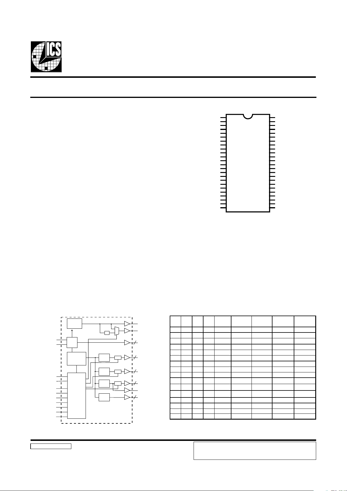
Pin Configuration
48-Pin 300mil SSOP
* These inputs have a 120K pull down to GND.
1
These are double strength.
Frequency Generator & Integrated Buffers for Celeron & PII/III™
VDDA
(AGPSEL)REF0
*(FS3)REF1
GND
X1
X2
VDDPCI
*(FS1)PCICLK_F
*(FS2)PCICLK0
PCICLK1
PCICLK2
PCICLK3
PCICLK4
GND
VDDAGP
AGPCLK0
AGPCLK1
GND
GND
*(FS0)48MHz
*(MODE)24_48MHz
VDD48
S DATA
SCLK
1
1
*
VDDL
CPUCLK0
CPUCLK1
CPUCLK2
GND
VDDSDR
SDRAM0
SDRAM1
SDRAM2
GND
SDRAM3
SDRAM4
SDRAM5
VDDSDR
SDRAM6
SDRAM7
GND
SDRAM8/PD#
SDRAM9/SDRAM_STOP#
GND
SDRAM10/PCI_STOP#
SDRAM11/CPU_STOP#
SDRAM12
VDDSDR
ICS9248-146
1
2
3
4
5
6
7
8
9
10
11
12
13
14
15
16
17
18
19
20
21
22
23
24
48
47
46
45
44
43
42
41
40
39
38
37
36
35
34
33
32
31
30
29
28
27
26
25
PLL2
PLL1
Spread
Spectrum
48MHz
24_48MHz
CPUCLK (2:0)
SDRAM (12:0)
PCICLK (4:0)
AGP (1:0)
PCICLK_F
2
5
13
3
2
X1
X2
XTAL
OSC
CPU
DIVDER
SDRAM
DIVDER
PCI
DIVDER
Stop
Stop
Stop
S DATA
SCLK
FS(3:0)
PD#
PCI_STOP#
CPU_STOP#
SDRAM_STOP#
MODE
AGP_SEL
Control
Logic
Config.
Reg.
/ 2
REF(1:0)
AGP
DIVDER
0 0 0 0 66.67 66.67 33.33 66.67 50.00
0 0 0 1 100.00 100.00 33.33 66.67 50.00
0 0 1 0 166.67 166.67 33.33 66.66 55.56
0 0 1 1 133.33 133.33 33.33 66.67 50.00
0 1 0 0 66.67 100.00 33.33 66.67 50.00
0 1 0 1 100.00 66.67 33.33 66.67 50.00
0 1 1 0 100.00 133.33 33.33 66.67 50.00
0 1 1 1 133.33 100.00 33.33 66.67 50.00
1 0 0 0 112.00 112.00 33.60 67.20 56.00
1 0 0 1 124.00 124.00 31.00 62.00 46.50
1 0 1 0 138.00 138.00 34.50 69.00 51.75
1 0 1 1 150.00 150.00 30.00 60.00 50.00
1 1 0 0 66.67 133.33 33.33 66.67 50.00
1 1 0 1 100.00 150.00 30.00 60.00 50.00
1 1 1 0 150.00 100.00 30.00 60.00 50.00
1 1 1 1 160.00 120.00 30.00 60.00 48.00
FS3 FS2 FS1 FS0 CPU SDRAM PCICLK
AGP SEL
= 0
AGP SEL
= 1
ICS reserves the right to make changes in the device data identified in
this publication without further notice. ICS advises its customers to
obtain the latest version of all device data to verify that any
information being relied upon by the customer is current and accurate.
Page 2
2
ICS9248-146
Third party brands and names are the property of their respective owners.
The ICS9248-146 is the single chip clock solution for
Desktop/Notebook designs using the SIS 630S style chipset.
It provides all necessary clock signals for such a system.
Spread spectrum may be enabled through I2C programming.
Spread spectrum typically reduces system EMI by 8dB to
10dB. This simplifies EMI qualification without resorting to
board design iterations or costly shielding. The ICS9248-146
employs a proprietary closed loop design, which tightly
controls the percentage of spreading over process and
temperature variations.
Serial programming I2C interface allows changing functions,
stop clock programming and frequency selection.
General Description
Pin Configuration
Power Groups
Analog
VDDA = X1, X2, Core, PLL
VDD48 = 48MHz, 24MHz, fixed PLL
Digital
VDDPCI = PCICLK_F , PCICLK
VDDSDR = SDRAM
VDDAGP=AGP , REF
EDOM
12niP
72niP82niP03niP13niP
011MARDS01MARDS9MARDS8MARDS
1#POTS_UPC#POTS_ICP#POTS_MARDS#DP
MODE Pin Power Management Control Input
PIN NUMBER PIN NAME TYPE DESCRIPTION
1, 7, 15, 22, 25,
35, 43
VDD PWR
3.3V Pow er supply for S DRAM output buffers, PCI output buffers,
reference out
p
ut buffers and 48M Hz output
AGPSEL IN AG P frequency select pin.
REF0 OUT 14.318 MHz reference clock.
FS3 IN Frequency select pin.
REF1 OUT 14.318 MHz reference clock.
4, 14, 18, 19, 29,
32, 39, 44
GN D PWR Ground pin for 3V outputs.
5 X1 IN Crystal input,nominally 14.318M Hz.
6 X2 OUT Crystal output, nominally 14.318M Hz.
FS1 IN Frequency select pin.
PCICLK_F OUT PCI clock output, not affected by P CI_STOP#
FS2 IN Frequency select pin.
PCICLK0 OUT PCI clock output.
13, 12, 11, 10 PCICLK (4:1) OUT PCI clock outputs.
17, 16, AGP (1:0) OU T AG P outputs defined as 2X PCI. These may not be stopped.
FS0 IN Frequency select pin.
48MH z OUT 48MH z output clock
MODE IN
Pin 27, 28, 30, & 31 function select pins
0=Deskto
p
1=Mobile mode
24_48MH z OUT Clock output for super I/O/USB default is 24M Hz
23 SDATA I/O
Data
p
in for I2C circuitry 5V tolerant
24 SCLK IN
Clock
p
in of I2C circuitry 5V tolerant
CPU_STOP# IN
Stops all PCICLK s besides the PCICLK_F clocks at logic 0 level, when input
is low and M ODE
p
in is in M ob ile mode
SDRAM11 OUT SD RAM clock output
PCI_STOP# IN
Stops all CPUCLKs clocks at logic 0 level, when input is low and M OD E pin
is in M obile mode
SDRAM10 OUT SD RAM clock output
SDR AM 9 OU T SD RAM clock output
SDRAM_STOP# IN
Stops all SD RAM clocks at logic 0 level, when input is low and MOD E pin
is in M obile mode
PD# IN
Asynchronous active low input pin used to pow er down the device into a low
pow er state. The internal clocks are disabled and the VCO and the crys tal are
stopped. The latency of the power down will not be greater than 3ms.
SDR AM 8 OU T SD RAM clock output
26 33, 34, 36, 37,
38, 40, 41, 42
SDRAM (12, 7:0) OUT SDRAM clock outputs
45, 46, 47 CPUCLK (2:0) OUT CPU clock outputs.
48 VD DL PWR Pow er pin for the CPUCLKs. 2.5V
31
20
2
8
9
21
3
30
27
28
Page 3
3
ICS9248-146
Third party brands and names are the property of their respective owners.
Byte0: Functionality and Frequency Select Register (default = 0)
Serial Configuration Command Bitmap
Note: PWD = Power-Up Default
Note1:
Default at power-up will be for latched logic inputs to define frequency, as displayed by Bit 3.
I
2
C is a trademark of Philips Corporation
tiBnoitpircseDDWP
2tiB
4:7tiB
2tiB
7tiB6tiB5tiB4tiB
00000
1etoN
3SF2SF1SF0SFUPCMARDSICP
PGA
0=LES
PGA
1=LES
egatnecerPdaerpS
0000 0 76.6676.6633.3376.6600.05daerpSnwoD%5.0-ot0
0000 1 00.00100.00133.3376.6600.05daerpSnwoD%5.0-ot0
000 10 76.66176.66133.3366.6665.55daerpSretneC%52.0-/+
000 1 1 33.33133.33133.3376.6600.05daerpSnwoD%5.0-ot0
0010 0 76.6600.00133.3376.6600.05daerpSnwoD%5.0-ot0
0010 1 00.00176.6633.3376.6600.05daerpSnwoD%5.0-ot0
00110 00.00133.33133.3376.6600.05daerpSnwoD%5.0-ot0
0011 1 33.33100.00133.3376.6600.05daerpSnwoD%5.0-ot0
01000 00.21100.21106.3302.7600.65daerpSretneC%52.0-/+
0100 1 00.42100.42100.1300.2605.64daerpSretneC%52.0-/+
01010 00.83100.83105.4300.9657.15daerpSretneC%52.0-/+
01011 00.05100.05100.0300.0600.05daerpSretneC%52.0-/+
01100 76.6633.33133.3376.6600.05daerpSnwoD%5.0-ot0
0110 1 00.00100.05100.0300.0600.05daerpSretneC%52.0-/+
01110 00.05100.00100.0300.0600.05daerpSretneC%52.0-/+
01111 00.06100.02100.0300.0600.84daerpSretneC%52.0-/+
1000 0 00.30100.30133.4376.8600.05daerpSretneC%52.0-/+
1000 1 03.00103.00134.3378.6600.05daerpSretneC%52.0-/+
100 1 0 00.00200.00233.3376.6600.05daerpSretneC%52.0-/+
100 1 1 37.33137.33134.3378.6651.05daerpSretneC%52.0-/+
1010 0 00.30133.73133.4376.8605.15daerpSretneC%52.0-/+
1010 1 33.73100.30133.4376.8605.15daerpSretneC%52.0-/+
101 1 0 78.6603.00134.3378.6651.05daerpSretneC%52.0-/+
101 1 1 37.33103.00134.3378.6651.05daerpSretneC%52.0-/+
1100 0 00.01100.01100.3300.6600.55daerpSretneC%52.0-/+
1100 1 00.51100.51105.4300.9605.75daerpSretneC%52.0-/+
110 1 0 00.04100.04100.5300.0705.25daerpSretneC%52.0-/+
110 1 1 05.10105.10138.3376.7600.05daerpSretneC%52.0-/+
1110 0 03.00137.33134.3378.6651.05daerpSretneC%52.0-/+
1110 1 00.50100.04100.5300.0705.25daerpSretneC%52.0-/+
11110 00.50105.75105.1300.3605.25daerpSretneC%52.0-/+
1111 1 33.53105.10138.3376.7657.05daerpSretneC%52.0-/+
3tiB
stupnIdehctaL,tceleserawdrahybdetcelessiycneuqerF-0
4:72,tiBybdetcelessiycneuqerF-1
0
1tiB
lamroN-0
delbanEmurtcepSdaerpS-1
1
0tiB
gninnuR-0
stuptuollaetatsirT-1
0
Page 4
4
ICS9248-146
Third party brands and names are the property of their respective owners.
Byte 1: CPU, Active/Inactive Register
(1= enable, 0 = disable)
Byte 2: PCI, Active/Inactive Register
(1= enable, 0 = disable)
TIB#NIPDWPNOITPIRCSED
7tiB-1 devreseR
6tiB-1 devreseR
5tiB311 4KLCICP
4tiB211 3KLCICP
3tiB111 2KLCICP
2tiB011 1KLCICP
1tiB91 0KLCICP
0tiB81 F_KLCICP
Notes:
1. Inactive means outputs are held LOW and are disabled
from switching.
2. Latched Frequency Selects (FS#) will be inverted logic
load of the input frequency select pin conditions.
TIB#NIPDWPNOITPIRCSED
7tiB-1 devreseR
6tiB121 zHM84_42
5tiB021 zHM84
4tiB621 21MARDS
3tiB721 11MARDS
2tiB821 01MARDS
1tiB031 9MARDS
0tiB131 8MARDS
Byte 4: SDRAM , Active/Inactive Register
(1= enable, 0 = disable)
TIB#NIPDWPNOITPIRCSED
7tiB-X )kcabdaeR(3SF
6tiB-X )kcabdaeR(2SF
5tiB-X )kcabdaeR(1SF
4tiB-X )kcabdaeR(0SF
3tiB211FER
2tiB310FER
1tiB711 1KLCPGA
0tiB611 0KLCPGA
Byte 5: AGP, Active/Inactive Register
(1= enable, 0 = disable)
Byte 3: SDRAM, Active/Inactive Register
(1= enable, 0 = disable)
TIB#NIPDWPNOITPIRCSED
7tiB331 7MARDS
6tiB431 6MARDS
5tiB631 5MARDS
4tiB731 4MARDS
3tiB831 3MARDS
2tiB041 2MARDS
1tiB141 1MARDS
0tiB241 0MARDS
TIB#NIPDWPNOITPIRCSED
7tiB-1
84_42leS
)zHM84:0,zHM42:1(
6tiB-1 devreseR
5tiB-1 devreseR
4tiB-1 devreseR
3tiB741 0KLCUPC
2tiB641 1KLCUPC
1tiB541 2KLCUPC
0tiB-1 devreseR
Page 5
5
ICS9248-146
Third party brands and names are the property of their respective owners.
Byte 6: Control , Active/Inactive Register
(1= enable, 0 = disable)
TIB#NIPDWPNOITPIRCSED
7tiB-0 devreseR
6tiB-0 devreseR
5tiB-1 devreseR
4tiB-0 devreseR
3tiB-1 devreseR
2tiB-0 devreseR
1tiB-0 devreseR
0tiB-1 devreseR
Byte 7: Vendor ID Register
(1= enable, 0 = disable)
TIB#NIPDWPNOITPIRCSED
7tiB3,20 X2=1,X1=0htgnertsFER
6tiB540
lortnoC-potS-2KLCUPC
,2KLCUPClortnoclliw#POTS_UPC=0
wolsi#POTS_UPCfinevegninnureerfsi2KLCUPC=1
5tiB-X )kcabdaeR(LESPGA
4tiB-X )kcabdaeR(EDOM
3tiB-X )kcabdaeR(#POTS_UPC
2tiB-X )kcabdaeR(#POTS_ICP
1tiB-X )kcabdaeR(#POTS_MARDS
0tiB-0
elggoTdeepSPGA
,gnittestupnihctalybdenimretedeblliw)2nip(LESPGA=0
gnittestupnihctalfoetisoppoeblliwLESPGA=1
Page 6

6
ICS9248-146
Third party brands and names are the property of their respective owners.
Absolute Maximum Ratings
Supply Voltage . . . . . . . . . . . . . . . . . . . . . . . . . . . . 5.5 V
Logic Inputs . . . . . . . . . . . . . . . . . . . . . . . . . . . . . . GND –0.5 V to V
DD
+0.5 V
Ambient Operating Temperature . . . . . . . . . . . . . 0°C to +70°C
Case Temperature. . . . . . . . . . . . . . . . . . . . . . . . . . 115°C
Storage Temperature . . . . . . . . . . . . . . . . . . . . . . . –65°C to +150°C
Stresses above those listed under Absolute Maximum Ratings may cause permanent damage to the device. These ratings are
stress specifications only and functional operation of the device at these or any other conditions above those listed in the
operational sections of the specifications is not implied. Exposure to absolute maximum rating conditions for extended periods
may affect product reliability.
Electrical Characteristics - Input/Supply/Common Output Parameters
TA = 0 - 70º C; Supply Volt age VDD = 3.3 V +/-5%VD DL = 2.5 V +/-5% (unless otherwise stated)
PARAMETER SYMBOL CONDITION S MIN TYP MAX UNITS
Input High Voltage V
IH
2V
DD
+0.3 V
Input Low Voltage V
IL
VSS-0.3 0.8 V
Supply Current I
DD
CL=30 pF, CPU @ 66, 100 MHz 390 400 mA
Power Down PD 300 600
µ
A
Input frequency Fi VDD = 3.3 V; 12 14.318 16 MHz
Inp u t Capacita n c e1 C
IN
Logic Inputs 5 pF
C
INX
X1 & X2 pins 27 45 pF
Transition Time T
trans
To 1st crossing of target Freq. 3
Settling Time T
S
From 1st crossing to 1% target Freq.
Clk Stabilization
1
T
STAB
From VDD= 3.3 V to 1% target Freq. 3 ms
Skew T
CPU-PCI
CPUVT= 1.5 V PCI VT=1.25V 1 1.9 4 ns
Skew
T
CPU-SDRAM
CPUVT= 1.5 V SDRAM VT=1.25
-500 -300 0 ps
1
Guaranteed by design, not 100% tested in production.
Page 7

7
ICS9248-146
Third party brands and names are the property of their respective owners.
Electrical Characteristics - CPU
TA = 0 - 70C; V
DDL
= 2.5 V +/-5%; VDDL = 2.5 V +/-5%; CL = 10-20 pF (unless otherwise specified)
PARAMETER SYMBOL CONDITIONS MIN TYP MAX UNITS
Out
p
ut Impedance
1
R
DSP2B
VO = VDD*(0.5)
10 20
Ω
Out
p
ut Impedance
1
R
DSN2B
VO = VDD*(0.5)
10 20
Ω
Output High Voltage
V
OH2B
IOH = -12.0 mA
2V
Output Low Voltage
V
OL2B
IOL = 12 mA
0.4 V
Output Hig h Cu r rent
I
OH2B
V
OH
= 1.7 V
-19 mA
Output Low Current
I
OL2B
V
O
L
= 0.7 V
19 mA
Rise Time
1
t
r2B
VOL = 0.4 V, VOH = 2.0 V
0.4 1.2 1.6 ns
Fall Time
1
t
f2B
VOH = 2.0 V, VOL = 0.4 V
0.4 1.1 1.6 ns
Duty Cycle
1
d
t2B
VT = 1.25 V
45 46.9 55 %
Skew window
0:1
t
sk2B
VT = 1.25 V
43 175 ps
Skew window
0:2
t
sk2B
VT = 1.25 V
142 375 ps
Jitter, Cycle-to-cycle
1
t
jcyc-cyc
VT = 1.25 V, CPU=66 MHz
177 250 ps
1
Guaranteed by design, not 100% tested in production.
Electrical Characteristics - 24-48MHz
TA = 0 - 70C; VDD = 3.3 V +/-5%;VDDL = 2.5 V +/-5%; CL = 10-20 pF (unless otherwise specified)
PARAMETER SYMBOL CONDITIONS MIN TYP MAX UNITS
Output Impedance R
DSP5B
1
VO = VDD*(0.5) 20 60
Ω
Output Impedance R
DSN5B
1
VO = VDD*(0.5) 20 60
Ω
Output High Voltage V
OH15
IOH = -14 mA 2.4 V
Output Low Voltage V
OL5
IOL = 6.0 mA 0.4 V
Output High Current
I
OH5
V
OH
= 2.0 V -20
mA
Output Low Current
I
OL5
V
OL
= 0.8 V 10
mA
Rise Time
1
t
r5
VOL = 0.4 V, VOH = 2.4 V 0.4 1.45 4 ns
Fall Time
1
t
f5
VOH = 2.4 V, VOL = 0.4 V 0.4 1.5 4 ns
Duty Cycle
1
d
t5
VT = 1.5 V 45 52.5 55 %
Jitter
t
cycle to cycleVT
= 1.5 V
210 500 ps
1
Guaranteed by design, not 100% tested in production.
Page 8

8
ICS9248-146
Third party brands and names are the property of their respective owners.
Electrical Characteristics - PCI
TA = 0 - 70C; VDD = 3.3 V +/-5%; VDDL = 2.5 V +/-5%; CL = 10-30 pF (unless otherwise specified)
PARAMETER SYMBOL CONDITIONS MIN TYP MAX UNITS
Output Impedance R
DSP1B
1
VO = VDD*(0.5) 12 55
Ω
Output Impedance R
DSN1B
1
VO = VDD*(0.5) 12 55
Ω
Output High Voltage V
OH1
IOH = -1 mA 2.4 V
Output Low Voltage V
OL1
IOL = 1 mA 0.55 V
Output High Current
I
OH1
V
OH @ MIN
= 1.0 V -29
mA
Output Low Current
I
OL1
V
OL @ MIN
= 1.95 V 29
mA
Rise Time
1
t
r1
VOL = 0.4 V, VOH = 2.4 V 0.5 2.3 2.5 ns
Fall Time
1
t
f1
VOH = 2.4 V, VOL = 0.4 V 0.5 2.3 2.5 ns
Duty Cycle
1
d
t1
VT = 1.5 V 45 51.2 55 %
Skew window
1
t
sk1
VT = 1.5 V 108 500 ps
Jitter, Cycle-to-cycle
1
t
jcyc-cyc1
VT = 1.5 V
353 500 ps
1
Guaranteed by design, not 100% tested in production.
Electrical Characteristics - SDRAM
TA = 0 - 70C; VDD = 3.3 V +/-5%;VDDL = 2.5 V +/-5%; CL = 20-30 pF (unless otherwise specified)
PARAMETER SYMBOL CONDITIONS MIN TYP MAX UNITS
Output Impedance R
DSP3B
1
VO = VDD*(0.5) 10 24
Ω
Output Impedance R
DSN3B
1
VO = VDD*(0.5) 10 24
Ω
Output High Voltage V
OH3
IOH = -18 mA 2.4 V
Output Low Voltage V
OL3
IOL = 9.4 mA 0.4 V
Output High Curre nt
I
OH3
V
OH
= 2.0 V -46
mA
Output Low Current
I
OL3
V
OL
= 0.8V
mA
Rise Time
1
t
r3
VOL = 0.4 V, VOH = 2.4 V 0.8 1.6 ns
Fall Time
1
t
f3
VOH = 2.4 V, VOL = 0.4 V 0.8 1.6 ns
Duty Cycle
1
d
t3
VT = 1.5 V 45 48.5 55 %
Skew window
1(0:11)
t
sk3
VT = 1.5 V 192 250 ps
Skew window
1( 0:12)
t
sk3
VT = 1.5 V 290 500 ps
Jitter, Cycle-to-cycle
1
t
jcyc-cyc3
VT = 1.5 V, CPU=66,100,133 MHz
173 250
ps
1
Guaranteed by design, not 100% tested in production.
Page 9

9
ICS9248-146
Third party brands and names are the property of their respective owners.
Electrical Characteristics - REF
TA = 0 - 70º C; VDD = 3.3 V +/-5%;VDDL = 2.5 V +/-5%; CL = 20 pF (unless otherwise stated)
PARAMETER SYMBOL CONDITIONS MIN TYP MAX UNITS
Output High Voltage V
OH5
I
OH
= -12 mA 2.4 V
Output Low Voltage V
OL5
IOL = 9 mA 0.4 V
Output High Current I
OH5
VOH = 2.0 V -22 mA
Output Low Current I
OL5
VOL = 0.8 V 16 mA
Rise Time
1
t
r5
VOL = 0.4 V, VOH = 2.4 V 1.8 4 ns
Fall Time
1
t
f5
VOH = 2.4 V, VOL = 0.4 V 1.9 4 ns
Duty Cycle
1
d
t5
VT = 50%
45 54.5 55 %
1
Guaranteed by design, not 100% tested in production.
Electrical Characteristics - AGP
TA = 0 - 70C; VDD=3.3V +/-5%; CL = 20 pF (unless otherwise specified)
PARAMETER SYMBOL CONDITIONS MIN TYP MAX UNITS
Output Impedance R
DSP4B
1
VO=VDD*(0.5) 12 55 Ω
Output Impedance R
DSN4B
1
VO=VDD*(0.5) 12 55 Ω
Output High Volt age V
OH4B
IOH = -18 mA 2 V
Output Low Voltage V
OL4B
IOL = 18 mA 0.4 V
Output High Current
I
OH4B
VOH = 2.0 V -19
mA
Output Low Current
I
OL4B
VOL = 0.8 V 19
mA
Rise Time
1
t
r4B
VOL = 0.4 V, VOH = 2.4 V 0.5 1.5 2 ns
Fall Time
1
t
f4B
VOH = 2.4 V, VOL = 0.4 V 0.5 1.6 2 ns
Duty Cycle
1
d
t4B
VT = 1.5 V 45 52.3 55 %
Skew window1
tsk
1
VT = 1.5 V 55.5 175 ps
Jitter Cyc-Cyc
tjcyc-cyc
1
VT = 1.5 V
239 500 ps
1
Guaranteed by design, not 100% tested in production.
Page 10

10
ICS9248-146
Third party brands and names are the property of their respective owners.
1. The ICS clock generator is a slave/receiver, I2C component. It can read back the data stored in the latches for
verification. Read-Back will support Intel PIIX4 "Block-Read" protocol.
2. The data transfer rate supported by this clock generator is 100K bits/sec or less (standard mode)
3. The input is operating at 3.3V logic levels.
4. The data byte format is 8 bit bytes.
5. To simplify the clock generator I
2
C interface, the protocol is set to use only "Block-Writes" from the controller. The
bytes must be accessed in sequential order from lowest to highest byte with the ability to stop after any complete byte
has been transferred. The Command code and Byte count shown above must be sent, but the data is ignored for those
two bytes. The data is loaded until a Stop sequence is issued.
6. At power-on, all registers are set to a default condition, as shown.
Controller (Host)
ICS (Slave/Receive r)
Start Bit
Address
D2
(H)
ACK
Dumm y Com m and C ode
ACK
Dumm y B y t e Count
ACK
Byte 0
ACK
Byte 1
ACK
Byte 2
ACK
Byte 3
ACK
Byte 4
ACK
Byte 5
ACK
Byte 6
ACK
Byte 7
ACK
Stop Bit
How to Write:
Controller (Host)
ICS (Slave /Rece ive r)
Start Bit
Address
D3
(H)
ACK
Byte Count
ACK
Byte 0
ACK
Byte 1
ACK
Byte 2
ACK
Byte 3
ACK
Byte 4
ACK
Byte 5
ACK
Byte 6
ACK
Byte 7
Stop Bit
How to Read:
General I2C serial interface information
The information in this section assumes familiarity with I2C programming.
For more information, contact ICS for an I
2
C programming application note.
How to Write:
• Controller (host) sends a start bit.
• Controller (host) sends the write address D2
(H)
• ICS clock will acknowledge
• Controller (host) sends a dummy command code
• ICS clock will acknowledge
• Controller (host) sends a dummy byte count
• ICS clock will acknowledge
• Controller (host) starts sending first byte (Byte 0)
through byte 6
• ICS clock will acknowledge each byte one at a time.
• Controller (host) sends a Stop bit
How to Read:
• Controller (host) will send start bit.
• Controller (host) sends the read address D3
(H)
• ICS clock will acknowledge
• ICS clock will send the byte count
• Controller (host) acknowledges
• ICS clock sends first byte (Byte 0) through byte 7
• Controller (host) will need to acknowledge each byte
• Controller (host) will send a stop bit
Notes:
Page 11

11
ICS9248-146
Third party brands and names are the property of their respective owners.
Fig. 1
Shared Pin Operation Input/Output Pins
The I/O pins designated by (input/output) on the ICS9248146 serve as dual signal functions to the device. During initial
power-up, they act as input pins. The logic level (voltage)
that is present on these pins at this time is read and stored
into a 5-bit internal data latch. At the end of Power -On reset,
(see AC characteristics for timing values), the device changes
the mode of operations for these pins to an output function.
In this mode the pins produce the specified buffered clocks
to external loads.
T o program (load) the internal configuration register for these
pins, a resistor is connected to either the VDD (logic 1) power
supply or the GND (logic 0) voltage potential. A 10 Kilohm
(10K) resistor is used to provide both the solid CMOS
programming voltage needed during the power-up
programming period and to provide an insignificant load on
the output clock during the subsequent operating period.
Via to
VDD
Clock trace to load
Series Term. Res.
Programming
Header
Via to Gnd
Device
Pad
2K
8.2K
Figure 1 shows a means of implementing this function when
a switch or 2 pin header is used. With no jumper is installed
the pin will be pulled high. With the jumper in place the pin
will be pulled low. If programmability is not necessary, than
only a single resistor is necessary. The programming resistors
should be located close to the series termination resistor to
minimize the current loop area. It is more important to locate
the series termination resistor close to the driver than the
programming resistor.
Page 12

12
ICS9248-146
Third party brands and names are the property of their respective owners.
CPU_STOP# Timing Diagram
CPU_STOP# is an asychronous input to the clock synthesizer. It is used to turn off the CPU clocks for low power operation.
CPU_STOP# is synchronized by the ICS9248-146. The minimum that the CPU clock is enabled (CPU_STOP# high pulse) is 100
CPU clocks. All other clocks will continue to run while the CPU clocks are disabled. The CPU clocks will always be stopped in
a low state and start in such a manner that guarantees the high pulse width is a full pulse. CPU clock on latency is less than 4
CPU clocks and CPU clock off latency is less than 4 CPU clocks.
Notes:
1. All timing is referenced to the internal CPU clock.
2. CPU_STOP# is an asynchronous input and metastable conditions may exist. This signal is synchronized
to the CPU clocks inside the ICS9248-146.
3. All other clocks continue to run undisturbed. (including SDRAM outputs).
Page 13

13
ICS9248-146
Third party brands and names are the property of their respective owners.
PCI_STOP# Timing Diagram
PCI_STOP# is an asynchronous input to the ICS9248-146. It is used to turn off the PCICLK clocks for low power operation.
PCI_STOP# is synchronized by the ICS9248-146 internally. The minimum that the PCICLK clocks are enabled (PCI_STOP#
high pulse) is at least 10 PCICLK clocks. PCICLK clocks are stopped in a low state and started with a full high pulse width
guaranteed. PCICLK clock on latency cycles are only one rising PCICLK clock off latency is one PCICLK clock.
Notes:
1. All timing is referenced to the Internal CPUCLK (defined as inside the ICS9248-146 device.)
2. PCI_STOP# is an asynchronous input, and metastable conditions may exist. This signal is required to be synchronized
inside the ICS9248-146.
3. All other clocks continue to run undisturbed.
4. CPU_STOP# is shown in a high (true) state.
Page 14

14
ICS9248-146
Third party brands and names are the property of their respective owners.
SDRAM_STOP# Timing Diagram
SDRAM_STOP# is an asychronous input to the clock synthesizer. It is used to stop SDRAM clocks for low power operation.
SDRAM_STOP# is synchronized to complete it's current cycle, by the ICS9248-146. All other clocks will continue to run while
the SDRAM clocks are disabled. The SDRAM clocks will always be stopped in a low state and start in such a manner that
guarantees the high pulse width is a full pulse.
Notes:
1. All timing is referenced to the internal CPU clock.
2. SDRAM is an asynchronous input and metastable conditions may exist. This signal is synchronized to
the SDRAM clocks inside the ICS9248-146.
3. All other clocks continue to run undisturbed.
Page 15

15
ICS9248-146
Third party brands and names are the property of their respective owners.
PD# Timing Diagram
The power down selection is used to put the part into a very low power state without turning off the power to the part. PD# is
an asynchronous active low input. This signal needs to be synchronized internal to the device prior to powering down the clock
synthesizer.
Internal clocks are not running after the device is put in power down. When PD# is active low all clocks need to be driven to a
low value and held prior to turning off the VCOs and crystal. The power up latency needs to be less than 3 mS. The power down
latency should be as short as possible but conforming to the sequence requirements shown below. PCI_STOP# and
CPU_STOP# are considered to be don't cares during the power down operations. The REF and 48MHz clocks are expected to
be stopped in the LOW state as soon as possible. Due to the state of the internal logic, stopping and holding the REF clock
outputs in the LOW state may require more than one clock cycle to complete.
Notes:
1. All timing is referenced to the Internal CPUCLK (defined as inside the ICS9248-146 device).
2. As shown, the outputs Stop Low on the next falling edge after PD# goes low.
3. PD# is an asynchronous input and metastable conditions may exist. This signal is synchronized inside this part.
4. The shaded sections on the VCO and the Crystal signals indicate an active clock.
5. Diagrams shown with respect to 133MHz. Similar operation when CPU is 100MHz.
Page 16

16
ICS9248-146
Third party brands and names are the property of their respective owners.
Ordering Information
ICS9248yF-146-T
Designation for tape and reel packaging
Pattern Number (2 or 3 digit number for parts with ROM code patterns)
Package Type
F=SSOP
Revision Designator (will not correlate with datasheet revision)
Device Type
Prefix
ICS, AV = S tandard Device
Example:
ICS XXXX y F - PPP - T
ICS reserves the right to make changes in the device data identified in
this publication without further notice. ICS advises its customers to
obtain the latest version of all device data to verify that any
information being relied upon by the customer is current and accurate.
INDEX
AREA
INDEX
AREA
12
1 2
N
D
h x 45°
h x 45°
E1
E
SEATING
PLANE
SEATING
PLANE
A1
A
e
-C-
- C -
b
.10 (.004) C
.10 (.004) C
c
L
300 mil SSOP Package
MIN MAX MIN MAX
A 2.41 2.80 .095 .110
A1 0.20 0.40 .008 .016
b 0.20 0.34 .008 .0135
c 0.13 0.25 .005 .010
D
E 10.03 10.68 .395 .420
E1 7.40 7.60 .291 .299
e
h 0.38 0.64 .015 .025
L 0.50 1.02 .020 .040
N
α
0° 8° 0° 8°
MIN MAX MIN MAX
48 15.75 16.00 .620 .630
10-0034
SYMBOL
In Millimeters In Inches
COMMON DIMENSIONS COMMON DIMENSIONS
SEE VARIATIONS SEE VARIATIONS
0.635 BASIC 0.025 BASIC
Reference Doc.: JEDEC Publication 95, MO-118
VARIATIONS
SEE VARIATIONS SEE VARIATIONS
N
D mm. D (inch)
 Loading...