

Page 1
Integrated
Circuit
Systems, Inc.
ICS9248-131
Block Diagram
Pentium is a trademark of Intel Corporation
I2C is a trademark of Philips Corporation
9248-131 Rev B 7/17/00
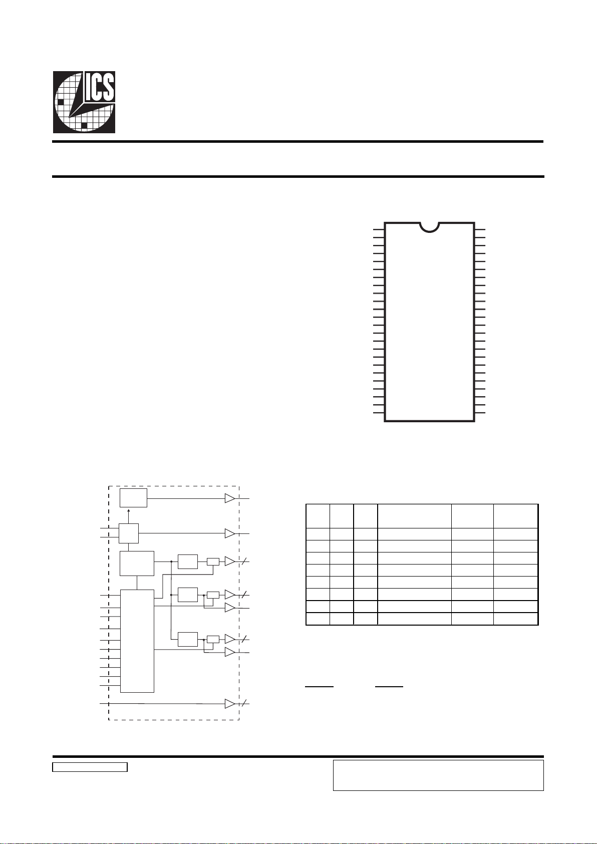
Pin Configuration
48-Pin SSOP
* Internal Pull-up Resistor of
240K to 3.3V on indicated inputs
VDDF
*REF0/CPU2.5_3.3#
GND
X1
X2
VDDPCI
*PCICLK_F/FS1
*PCICLK0/FS2
GND
PCICLK1
PCICLK2
PCICLK3
PCICLK4
VDDA
BUFFERIN
GND
*CPU_STOP#/SDRAM11
*PCI_STOP#/SDRAM10
VDDSDR
*AGP_STOP#/SDRAM9
*PD#/SDRAM8
GND
SDATA
SCLK
VDDAGP
AGP0
AGP1
GND
CPUCLK0
CPUCLK1
VDDL
CPUCLK2
SDRAM0
SDRAM1
VDDSDR
SDRAM2
SDRAM3
GND
SDRAM4
SDRAM5
VDDSDR
SDRAM6
SDRAM7
GND
48MHz/FS0*
AGP_F/MODE*
SDRAM12
GND
ICS9248-131
1
2
3
4
5
6
7
8
9
10
11
12
13
14
15
16
17
18
19
20
21
22
23
24
48
47
46
45
44
43
42
41
40
39
38
37
36
35
34
33
32
31
30
29
28
27
26
25
Recommended Application:
ALI - Aladdin V
- mobile style chipsets
Output Features:
3 - CPUs @ 2.5/3.3V, up to 100MHz.
3 - AGPCLK @ 3.3V
13 - SDRAM @ 3.3V
6 - PCI @ 3.3V
1 - 48MHz, @ 3.3V fixed.
1 - REF @ 3.3V, 14.318MHz.
Features:
Support power management: CPU, PCI, AGP stop and
Power down Mode from I2C programming.
Spread spectrum for EMI control.
Uses external 14.318MHz crystal
FS pins for frequency select
Key Specifications:
CPU CPU: <250ps
AGP PCI: <550ps
CPU(early)-PCI: 1-4ns, Center 2-6ns
Frequency Generator & Integrated Buffers for Celeron & PII/III™
CPU2.5_3.3#
PLL2
PLL1
Spread
Spectrum
48MHz
CPUCLK (2:0)
PCICLK (4:0)
AGP (1:0)
2
5
3
AGP_F
PCICLK_F
X1
X2
XTAL
OSC
CPU
DIVDER
PCI
DIVDER
AGP
DIVDER
Stop
Stop
Stop
SDATA
SCLK
FS (2:0)
PD#
PCI_STOP#
CPU_STOP#
SDRAM_STOP#
AGP-STOP#
MODE
Control
Logic
Config.
Reg.
REF
BUFFERIN
SDRAM (12:0)
13
1 1 1 100 33.33 66.67
1 1 0 95.25 31.75 63.50
1 0 1 83.3 33.30 66.60
1 0 0 97 32.33 6 4.66
0 1 1 91.5 30.50 61.00
0 1 0 96.22 32.07 64.15
0 0 1 66.67 33.33 66.67
0 0 0 60 30.00 6 0.00
PCI
(MHz)
FS2 FS1 FS0
CPU, SDRAM
(MHz)
AGP
(MHz)
Functionality
Note: REF & IOAPIC = 14.318MHz
Power Groups
Analog Digital
VDDF VDDPCI
VDDA VDDSDR
VDDAGP
ICS reserves the right to make changes in the device data identified in
this publication without further notice. ICS advises its customers to
obtain the latest version of all device data to verify that any
information being relied upon by the customer is current and accurate.
Page 2
2
ICS9248-131
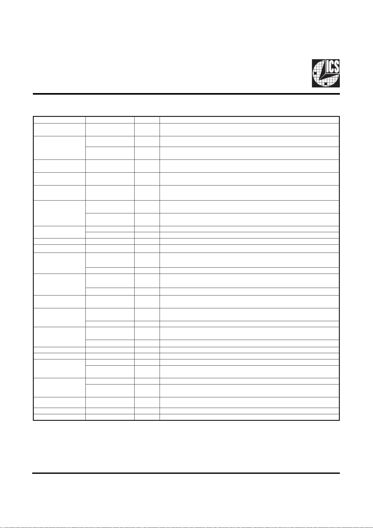
Pin Descriptions
Notes:
1: Internal Pull-up Resistor of 240K to 3.3V on indicated inputs
2: Bidirectional input/output pins, input logic levels are latched at internal power-on-reset. Use 10Kohm resistor to
program logic Hi to VDD or GND for logic low.
REBMUNNIPEMANNIPEPYTNOITPIRCSED
,91,41,6,1
84,63,03
DDVRWPV3.3lanimon,ylppusrewoP
2
0FERTUO.kcolcecnereferzhM813.41
#3.3_5.2UPC
2,1
NI
V3.3=WOL,UPCV5.2=hgiH.V5.2roV3.3siLDDVrehtehwsetacidnI
UPC
1
tupnidehctaL.
2
,72,22,61,9,3
54,93,33
DNGRWPdnuorG
41XNI
kcabdeefdna)Fp33(pacdaollanretnisah,tupnilatsyrC
2Xmorfrotsiser
52XTUO
.zHM813.41yllanimon,tuptuolatsyrC
)Fp33(pacdaollanretnisaH
7
F_KLCICPTUO
wekssn4-1htiwsKLCUPChtiwsuonorhcnyS.tuptuokcolcICPgninnureerF
#POTS_ICPybdetceffatonsisihT)ylraeUPC(
1SF
2,1
NI
ehtsnimretedsnipSFrehtohtiwgnolA.tupnIdehctaL.niptcelesycneuqerF
.seicneuwerfPGA&ICP,MARDS,UPC
8
0KLCICPTUO )ylraeUPC(wekssn4-1htiwsKLCUPCsuonuorhcnyS.stuptuokcolcICP
2SF
2,1
NItupnIdehctaL.niptcelesycneuqerF
01,11,21,31)1:4(KLCICPTUO )ylraeUPC(wekssn4-1htiwsKLCUPCsuonuorhcnyS.stuptuokcolcICP
51NIREFFUBNI.sreffubMARDSrofniptupnI
71
#POTS_UPC
1
NI
,level0cigoltaskcolcKLCUPCstlaH
)0=EDOM,edoMeliboMni(woltupninehw
11MARDSTUOtuptuokcolcMARDS
81
#POTS_ICP
1
NI
woltupninehw,level0cigoltaskcolcKLCICPstlaH
)0=EDOM,edomelibomnI(
01MARDSTUOtuptuokcolcMARDS
,23,13,92,82,04
83,73,53,43
)0:7,21(MARDSTUO.stuptuokcolcMARDS
02
#POTS_PGANI
woltupninehwlevel"0"cigoltaskcolcPGAstlahtupnisuonorhcnysasihT
0PGAtceffatonseoD)0=EDOM,edoMeliboMni(
9MARDSTUOtuptuokcolcMARDS
12
#DPNI
lanretni&latsyrc,OCVehtspotStupninwoDrewoPsuonorehcnysasihT
)0=EDOM,edoMeliboMnI(.woL,evitcanehwskcolc
8MARDSTUOtuptuokcolcMARDS
32ATADSO/IIrofnipataD
2
tnarelotV5yrtiucricC
42KLCSNIIfonipkcolC
2
tnarelotV5yrtiucricC
52
F_PGATUO#POTS_PGAybdetceffatoN,tuptuotroPcihparGdecnavdA
EDOM
2,1
NI
.edoMeliboM=0,edoMpotkseD=1,niptcelesnoitcnuf12&02,81,71niP
.tupnIdehctaL
62
zHM84TUO.gnimitBSUrofkcolctuptuozHM84
0SF
2,1
NI
ehtsnimretedsnipSFrehtohtiwgnolA.tupnIdehctaL.niptcelesycneuqerF
.seicneuwerfPGA&ICP,MARDS,UPC
44,34,14)0:2(KLCUPCTUOwoL=#POTS_UPCfiwoL.LDDVybderewop,stuptuokcolcUPC
24LDDVRWPlanimonV3.3roV5.2rehtie,UPCrofylppuS
74,64)0:1(PGATUOstuptuotroPcihparGdecnavdA
Page 3
3
ICS9248-131
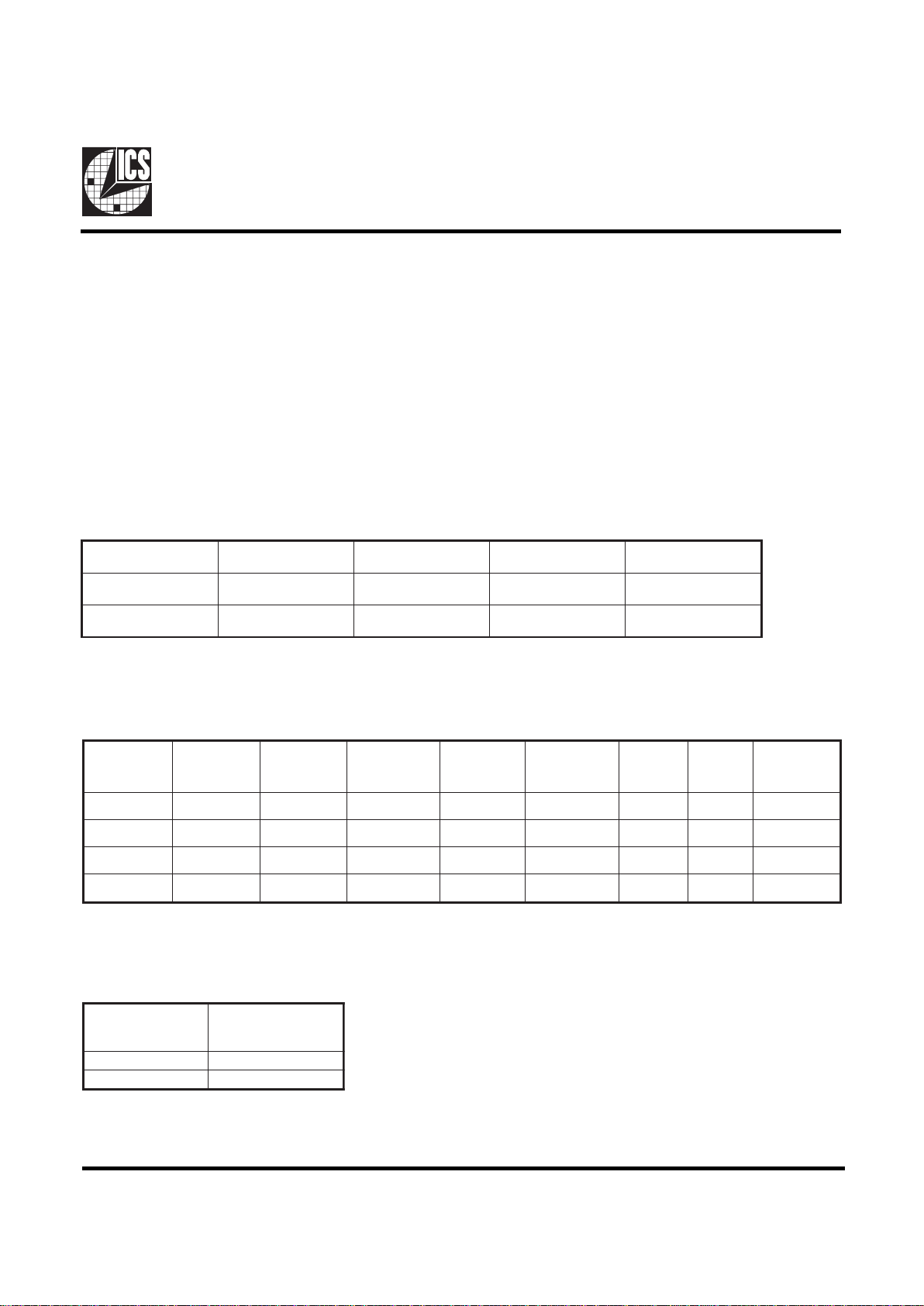
5.2_#3.3UPC
leveltupnI
)ataDdehctaL(
rofdetceleSreffuB
:tanoitarepo
1DDVV5.2
0DDVV3.3
CPU 3.3#_2.5V Buffer selector for CPUCLK drivers.
Power Management Functionality
Mode Pin - Power Management Input Control
52niP,EDOM
)tupnIdehctaL(
71niP81niP02niP12niP
0
#POTS_UPC
)TUPNI(
#POTS_ICP
)TUPNI(
#POTS_PGA
)TUPNI(
#DP
)TUPNI(
1
11MARDS
)TUPTUO(
01MARDS
)TUPTUO(
9MARDS
)TUPTUO(
8MARDS
)TUPTUO(
#POTS_PGA#POTS_UPC#POTS_ICP
,PGA
KLCUPC
stuptuO
KLCICP
)0:4(
,F_KLCICP
zHM84,FER
MARDSdna
latsyrC
CSO
OCV
PGA
)0:1(
101 woLdeppotSgninnuRgninnuRgninnuRgninnuRgninnuR
111 gninnuRgninnuRgninnuRgninnuRgninnuRgninnuR
110 gninnuRwoLdeppotSgninnuRgninnuRgninnuRgninnuR
011 gninnuRgninnuRgninnuRgninnuRgninnuRwoLdeppotS
General Description
The ICS9248-131 generates all clocks required for high speed RISC or CISC microprocessor systems such as Intel PentiumPro
or Cyrix. Eight different reference frequency multiplying factors are externally selectable with smooth frequency transitions.
Spread spectrum may be enabled through I2C programming. Spread spectrum typically reduces system EMI by 8dB to 10dB.
This simplifies EMI qualification without resorting to board design iterations or costly shielding. The ICS9248-131 employs a
proprietary closed loop design, which tightly controls the percentage of spreading over process and temperature variations.
Serial programming I2C interface allows changing functions, stop clock programming and frequency selection. The SDRAM12
output may be used as a feed back into an off chip PLL.
Page 4
4
ICS9248-131
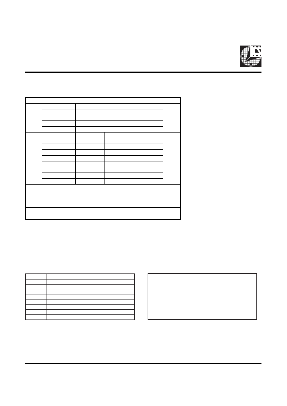
Byte0: Functionality and Frequency Select Register (default = 0)
Serial Configuration Command Bitmap
I2C is a trademark of Philips Corporation
Note 1. Default at Power-up will be for latched logic inputs to define frequency. Bits 4, 5, 6 are default to 001, and if bit
3 is written to a 1 to use Bits 6:4, then these should be defined to desired frequency at same write cycle.
Note: PWD = Power-Up Default
Byte 1: CPU, Active/Inactive Register
(1 = enable, 0 = disable)
Notes:
1. Inactive means outputs are held LOW and are disabled
from switching.
Notes:
1. Inactive means outputs are held LOW and are disabled
from switching.
tiB#niPDWPnoitpircseD
7tiB-1 )devreseR(
6tiB-X#2SF
5tiB-X#1SF
4tiB041 )tcanI/tcA(21MARDS
3tiB-1 )devreseR(
2tiB141 )tcanI/tcA(2KLCUPC
1tiB341 )tcanI/tcA(1KLCUPC
0tiB441 )tcanI/tcA(0KLCUPC
tiB#niPDWPnoitpircseD
7tiB-X #3.3_5.2UPC
6tiB71 )tcanI/tcA(F_KLCICP
5tiB-X#0SF
4tiB311 )tcanI/tcA(4KLCICP
3tiB211 )tcanI/tcA(3KLCICP
2tiB111 )tcanI/tcA(2KLCICP
1tiB011 )tcanI/tcA(1KLCICP
0tiB81 )tcanI/tcA(0KLCICP
Byte 2: PCI Active/Inactive Register
(1 = enable, 0 = disable)
Bit PWD
Bit7 Bit2
0,0
0,1
1,0
1,1
Bit6 Bit5 Bit4 CPU Clock PCI AGP
111 100 33.33 66.67
110 95.25 31.75 63.50
101 83.3 33.30 66.60
100 97 32.33 64.66
011 91.5 30.50 61.00
010 96.22 32.07 64.15
001 66.67 33.33 66.67
000 60 30.00 60.00
Bit 1
Bit 0
1 - Tristate all out
p
uts
0 - Frequency is selected by hardware select, Latched inputs
1 - Frequency is selected by Bit 6:4 (above)
0 to -0.5 Down Spread Spectrum Modulat ion
+/- 0.375% Center S
p
read Spectrum Modulation
0
0
0 - Normal
1 - Spread Spectrum Enabled
0 - Running
Description
Note1
001
Bit 3
Bit 6:4
Bit 7,2 0,0
Spread Spectrum Method
+/- 0.25% Center Spread Spectrum Modulation
+/- 0.15% Center Spread Spectrum Modulation
0
Page 5
5
ICS9248-131
Byte 3: SDRAM Active/Inactive Register
(1 = enable, 0 = disable)
Notes:
1. Inactive means outputs are held LOW and are disabled
from switching.
tiB#niPDWPnoitpircseD
7tiB821 )tcanI/tcA(7MARDS
6tiB921 )tcanI/tcA(6MARDS
5tiB131 )tcanI/tcA(5MARDS
4tiB231 )tcanI/tcA(4MARDS
3tiB431 )tcanI/tcA(3MARDS
2tiB531 )tcanI/tcA(2MARDS
1tiB731 )tcanI/tcA(1MARDS
0tiB831 )tcanI/tcA(0MARDS
Byte 4: SDRAM Active/Inactive Register
(1 = enable, 0 = disable)
Byte 5: Peripheral Active/Inactive Register
(1 = enable, 0 = disable)
Notes:
1. Inactive means outputs are held LOW and are disabled
from switching.
Notes:
1. Inactive means outputs are held LOW and are disabled
from switching.
tiB#niPDWPnoitpircseD
7tiB521 )evitcanI/evitcA(F_PGA
6tiB-1 )devreseR(
5tiB-1 )devreseR(
4tiB-1 )devreseR(
3tiB711
)tcanI/tcA(11MARDS
)ylnOedoMpotkseD(
2tiB811
)tcanI/tcA(01MARDS
)ylnOedoMpotkseD(
1tiB021 )tcanI/tcA(9MARDS
0tiB121 )tcanI/tcA(8MARDS
tiB#niPDWPnoitpircseD
7tiB-1 )devreseR(
6tiB-1 )devreseR(
5tiB-1 )devreseR(
4tiB741 )tcanI/tcA(0PGA
3tiB-1 )devreseR(
2tiB-XEDOM
1tiB641 )tcanI/tcA(1PGA
0tiB21 )tcanI/tcA(0FER
Byte 6: Optional Register for Possible
Furture Requirements
Notes:
1. Byte 6 is reserved by Integrated Circuit Systems for futue
applications.
tiB#niPDWPnoitpircseD
7tiB-1 )devreseR(
6tiB-1 )devreseR(
5tiB-1 )devreseR(
4tiB-1 )devreseR(
3tiB-1 )devreseR(
2tiB-1 )devreseR(
1tiB-1 )devreseR(
0tiB-1 )devreseR(
Page 6

6
ICS9248-131
Absolute Maximum Ratings
Supply Voltage . . . . . . . . . . . . . . . . . . . . . . . . . . . 5.5 V
Logic Inputs . . . . . . . . . . . . . . . . . . . . . . . . . . . . GND 0.5 V to VDD +0.5 V
Ambient Operating Temperature . . . . . . . . . . . . 0°C to +70°C
Storage Temperature . . . . . . . . . . . . . . . . . . . . . . 65°C to +150°C
Stresses above those listed under Absolute Maximum Ratings may cause permanent damage to the device. These ratings are
stress specifications only and functional operation of the device at these or any other conditions above those listed in the
operational sections of the specifications is not implied. Exposure to absolute maximum rating conditions for extended periods
may affect product reliability.
Electrical Characteristics - Input/Supply/Common Output Parameters
TA = 0 - 70º C; Supply Voltage VDD = 3.3 V +/-5%, V
DDL
=2.5V +/- 5% (unless otherwise stated)
PARAMETER SYMBOL CONDITIONS MIN TYP MAX UNITS
C
L
= 0 pF; Select @ 66.8 MHz 8 15
C
L
= 0 pF; Select @ 100 MHz 15 20
T
CPU-PCI1
Vt=1.5 V; f=66 / 100 Mhz; CP U leads 1 2 4 ns
T
AGP-PCI1
Vt = 1.5V; AGP Leads ( Vdd+/-5% 25C) 300 550 ps
Operatin g Supply Current
I
DDL2.5
mA
Skew
1
Electrical Characteristics - Input/Supply/Common Output Parameters
TA = 0 - 70º C; Supply Voltage VDD =V
DDL
= 3.3 V +/-5% (unless otherwise stated)
PARAMETER SYMBOL CONDITIONS MIN TYP MAX UNITS
Input High Voltage V
IH
2V
DD
+0.3 V
Input Low Voltage V
IL
VSS-0.3 0.8 V
Input High Current I
IH
VIN = V
DD
5
uA
Input Low Current I
IL1
VIN = 0 V; Inputs with no pull-up resistors -5
uA
Input Low Current I
IL2
VIN = 0 V; Inputs with pull-up resistors -200
uA
C
L
= 0 pF; Sele ct @ 66 MHz 105
160 mA
C
L
= 0 pF; Sele ct @ 100 MHz 140
160 mA
Input frequency F
i
VDD = 3.3 V 12 14.318 16 MHz
C
IN
Logic Inputs 5 pF
C
INX
X1 & X2 pins 27 45 pF
Transition Time
1
Ttrans To 1st crossing of target Freq 2 ms
Settlin
g
Time
1
Ts From 1st corssing to 1% t arget Freq 2 ms
Clk Stabilization
1
T
STAB
From VDD = 3.3 V to 1% target Freq. 2 ms
T
CPU-PCI
Vt=1.5 V; f=66 / 100 Mhz ; CPU leads 1 2 4 ns
T
AGP-PCI
Vt = 1.5V; A GP Leads ( Vdd+/-5% 25C) 300 550 ps
1
Guaranteed by design, not 100% tested in pr oduction.
Operatin g Supply Current
Input Capacitance
1
I
DD3.3OP
Skew
1
Page 7

7
ICS9248-131
Electrical Characteristics - CPU
TA = 0 - 70C; VDD=V
DDL
=3.3V +/- 5%; CL = 20 pF (unless otherwise specified)
PARAMETER SYMBOL CONDITIONS MIN TYP MAX UNITS
Output Impedance R
DSP2B
1
VO=VDD*(0.5) 13.5 30 45 Ω
Output Impedance R
DSN2B
1
VO=VDD*(0.5) 13.5 32 45 Ω
Output High Volt age V
OH2A
IOH = -28 mA 2.5 V
Output Low Voltage V
OL2A
IOL = 27 mA 0.4 V
Output High Current
I
OH2A
VOH = 2.0 V -23
mA
Output Low Current
I
OL2A
VOL = 0.8 V 33
mA
Rise Time
1
t
r2A
1
VOL = 0.4 V, VOH = 2.4 V 1.1 2 ns
Fall Time
1
t
f2A
1
VOH = 2.4 V, VOL = 0.4 V 1.6 2 ns
Duty Cycle
1
d
t2A
1
VT = 1.5 V 50 52 5 5
%
Skew window
1
t
sk2A
1
VT = 1.5 V 130 250 ps
Jitter, Cycle-to-cycle1
tjcyc-cyc2A
1
VT = 1.5 V 130 250 ps
1
Guaranteed by design, not 100% tested in production.
1
Edge displacement of a period relative to a 10-clock-cycle rolling average period.
Electrical Characteristics - CPU
TA = 0 - 70C; VDD=3.3V, V
DDL
=2.5V, both +/- 5%; CL = 20 pF (unless otherwise specified)
PARAMETER SYMBOL CONDITIONS MIN TYP MAX UNITS
Output Impedance R
DSP2B
1
VO=VDD*(0.5) 13.5 30 45 Ω
Output Impedance R
DSN2B
1
VO=VDD*(0.5) 13.5 32 45 Ω
Output High Volt age V
OH2B
IOH = -8 mA 2 V
Output Low Voltage V
OL2B
IOL = 12 mA 0.4 V
Output High Current
I
OH2B
VOH = 1.7 V -16
mA
Output Low Current
I
OL2B
VOL = 0.7 V 19
mA
Rise Time
1
t
r2B
1
VOL = 0.4 V, VOH = 2.0 V 1 1.8 ns
Fall Time
1
t
f2B
1
VOH = 2.0 V, VOL = 0.4 V 1.3 1.8 ns
Duty Cycle
1
d
t2B
1
VT = 1.25 V 45 50 55
%
Skew window
1
t
sk2B
1
VT = 1.25 V 130 250 ps
Jitter, Cycle-to-cycle1
tjcyc-cyc2A
1
VT = 1.5 V 130 250 ps
1
Guaranteed by design, not 100% tested in production.
1
Edge displacement of a period relative to a 10-clock-cycle rolling average period.
Page 8

8
ICS9248-131
Electrical Characteristics - PCI
TA = 0 - 70C; V
DD
= V
DDL
= 3.3V +/-5%; CL = 30 pF (unless otherwise specified)
PARAMETER SYMBOL CONDITIONS MIN TYP MAX UNITS
Output Impedance R
DSP2B
1
VO=VDD*(0.5) 12 24 55 Ω
Output Impedance R
DSN2B
1
VO=VDD*(0.5) 12 23 55 Ω
Output High Voltage V
OH1
IOH = -28 mA 2.4 V
Output Low Voltage V
OL1
IOL = 23 mA 0.4 V
Output High Current
I
OH1
VOH = 2.0 V -40
mA
Output Low Current
I
OL1
VOL = 0.8 V 41
mA
Rise Time
1
t
r1
VOL = 0.4 V, VOH = 2.4 V 1.7 2.3 ns
Fall Time
1
t
f1
VOH = 2.4 V, VOL = 0.4 V 1.5 2.0 ns
Duty Cycle
1
d
t1
VT = 1.5 V 45 50 55 %
Skew window
1
t
sk1
VT = 1.5 V 305 500 ps
Jitter, Cyc-to-Cyc
t
jcyc-cyc1
VT = 1.5 V
100 500 ps
1
Guaranteed by design, not 100% tested in production.
Electrical Characteristics - SDRAM
TA = 0 - 70C; VDD=V
DDL
=3.3V +/-5%; CL = 30 pF (unless otherwise specified)
PARAMETER SYMBOL CONDITIONS MIN TYP MAX UNITS
Output Impedance R
DSP2B
1
VO=VDD*(0.5) 12 24.19 55 Ω
Output Impedance R
DSN2B
1
VO=VDD*(0.5) 12 23.08 55 Ω
Output High Voltage V
OH1
IOH = -28 mA 2.4 V
Output Low Voltage V
OL1
IOL = 23 mA 0.4 V
Output High Current
I
OH1
VOH = 2.0 V -40
mA
Output Low Current
I
OL1
VOL = 0.8 V 41
mA
SD (0:1,3:12) Rise Time
1
t
r1
VOL = 0.4 V, VOH = 2.4 V 1.4 2 ns
SD(0:1,3:12) Fall Time
1
t
f1
VOH = 2.4 V, VOL = 0.4 V 1.5 2 ns
SD(0:1,3:12) Duty Cycle
1
d
t1
VT = 1.5 V 50 54 58 %
SD 2 Rise Time
1
t
r1
VOL = 0.4 V, VOH = 2.4 V 1.8 2.4 ns
SD 2 Fall Time
1
t
f1
VOH = 2.4 V, VOL = 0.4 V 1.9 2.4 ns
SD 2 Duty Cycle
1
d
t1
VT = 1.5 V 50 54 58 %
Propagation Delay Tprop
V
T
= 1.5 V 4 6 ns
Skew window
1
t
sk1
VT = 1.5 V
350 500 ps
1
Guaranteed by design, not 100% tested in production.
Page 9

9
ICS9248-131
Electrical Characteristics - AGP
TA = 0 - 70C; VDD=V
DDL
=3.3V +/-5%; CL = 30 pF (unless otherwise specified)
PARAMETER SYMBOL CONDITIONS MIN TYP MAX UNITS
Output Impedance R
DSP2B
1
VO=VDD*(0.5) 12 24.19 55 Ω
Output Impedance R
DSN2B
1
VO=VDD*(0.5) 12 23.08 55 Ω
Output High Volt age V
OH1
IOH = -28 mA 2.4 V
Output Low Voltage V
OL1
IOL = 23 mA 0.4 V
Output High Current
I
OH1
VOH = 2.0 V -40
mA
Output Low Current
I
OL1
VOL = 0.8 V 41
mA
Rise Time
1
t
r1
VOL = 0.4 V, VOH = 2.4 V 1.3 2 ns
Fall Time
1
t
f1
VOH = 2.4 V, VOL = 0.4 V 1.4 2 ns
Duty Cycle
1
d
t1
VT = 1.5 V 45 48 5 5 %
Skew window1 tsk1
V
T
= 1.5 V 100 250 ps
Jitter Cyc-Cyc, AGP(1:2)
tjcyc-cyc
1
VT = 1.5 V 120 250 ps
Jitter Cyc-Cyc, AGP_F
tjcyc-cyc
1
VT = 1.5 V
500 850 ps
1
Guaranteed by design, not 100% tested in production.
Electrical Characteristics - REF, 48MHz
TA = 0 - 70C; V
DD
= V
DDL
= 3.3V +/-5%; CL = 10 - 20 pF (unless otherwise specified)
PARAMETER SYMBOL CONDITIONS MIN TYP MAX UNITS
Output Impedance R
DSP2B
1
VO=VDD*(0.5) 20 47 60 Ω
Output Impedance R
DSN2B
1
VO=VDD*(0.5) 20 44 60 Ω
Output High Volt age V
OH5
IOH = -16 Ma 2.4 V
Output Low Voltage V
OL5
IOL = 9 mA 0.4 V
Output High Current
I
OH5
VOH = 2.0 V -22
mA
Output Low Current
I
OL5
VOL = 0.8 V 16
mA
Rise Time
1
t
r5
1
VOL = 0.4 V, VOH = 2.4 V 2.3 4.0 ns
Fall Time
1
t
f5
1
VOH = 2.4 V, VOL = 0.4 V 2.3 4.0 ns
Duty Cycle
1
d
t5
1
VT = 1.5 V 45 50 55 %
REF Jitter, Cyl-to-Cyl
t
j1s5
1
VT = 1.5 V
0.7 1 ns
1
Guaranteed by design, not 100% tested in production.
Page 10

10
ICS9248-131
Fig. 1
Shared Pin Operation Input/Output Pins
The I/O pins designated by (input/output) on the serve as
dual signal functions to the device. During initial power-up,
they act as input pins. The logic level (voltage) that is present
on these pins at this time is read and stored into a 5-bit
internal data latch. At the end of Power-On reset, (see AC
characteristics for timing values), the device changes the
mode of operations for these pins to an output function. In
this mode the pins produce the specified buffered clocks to
external loads.
To program (load) the internal configuration register for these
pins, a resistor is connected to either the VDD (logic 1) power
supply or the GND (logic 0) voltage potential. A 10 Kilohm
(10K) resistor is used to provide both the solid CMOS
programming voltage needed during the power-up
programming period and to provide an insignificant load on
the output clock during the subsequent operating period.
Via to
VDD
Clock trace to load
Series Term. Res.
Programming
Header
Via to Gnd
Device
Pad
2K
8.2K
Figure 1 shows a means of implementing this function when
a switch or 2 pin header is used. With no jumper is installed
the pin will be pulled high. With the jumper in place the pin
will be pulled low. If programmability is not necessary, than
only a single resistor is necessary. The programming resistors
should be located close to the series termination resistor to
minimize the current loop area. It is more important to locate
the series termination resistor close to the driver than the
programming resistor.
Page 11

11
ICS9248-131
1. The ICS clock generator is a slave/receiver, I2C component. It can read back the data stored in the latches for verification.
Read-Back will support Intel PIIX4 "Block-Read" protocol.
2. The data transfer rate supported by this clock generator is 100K bits/sec or less (standard mode)
3. The input is operating at 3.3V logic levels.
4. The data byte format is 8 bit bytes.
5. To simplify the clock generator I2C interface, the protocol is set to use only "Block-Writes" from the controller. The
bytes must be accessed in sequential order from lowest to highest byte with the ability to stop after any complete byte
has been transferred. The Command code and Byte count shown above must be sent, but the data is ignored for those
two bytes. The data is loaded until a Stop sequence is issued.
6. At power-on, all registers are set to a default condition, as shown.
General I2C serial interface information
The information in this section assumes familiarity with I2C programming.
For more information, contact ICS for an I2C programming application note.
How to Write:
Controller (host) sends a start bit.
Controller (host) sends the write address D2
(H)
ICS clock will acknowledge
Controller (host) sends a dummy command code
ICS clock will acknowledge
Controller (host) sends a dummy byte count
ICS clock will acknowledge
Controller (host) starts sending first byte (Byte 0)
through byte 5
ICS clock will acknowledge each byte one at a time.
Controller (host) sends a Stop bit
How to Read:
Controller (host) will send start bit.
Controller (host) sends the read address D3
(H)
ICS clock will acknowledge
ICS clock will send the byte count
Controller (host) acknowledges
ICS clock sends first byte (Byte 0) through byte 5
Controller (host) will need to acknowledge each byte
Controller (host) will send a stop bit
Notes:
Controller (Host) ICS (Slave/Receiver)
Start Bit
Address
D3
(H)
AC
K
Byte Count
ACK
Byte
0
ACK
Byte 1
ACK
Byte
2
ACK
Byte
3
ACK
Byte 4
ACK
Byte
5
ACK
Stop Bit
How to Read:
Controller (Host) ICS (Slave/Receiver)
Start Bit
Address
D2
(H)
AC
K
Dummy Command Code
AC
K
Dummy Byte Count
AC
K
Byte 0
AC
K
Byte 1
ACK
Byte 2
AC
K
Byte 3
AC
K
Byte 4
AC
K
Byte 5
AC
K
Stop Bit
How to Write:
Page 12

12
ICS9248-131
AGP_STOP# Timing Diagram
Notes:
1. All timing is referenced to the internal CPUCLK.
2. AGP_STOP# is an asynchronous input and metastable conditions may exist.
This signal is synchronized to the CPUCLKs inside the ICS9248-131.
3. All other clocks continue to run undisturbed.
4. PD# and PCI_STOP# are shown in a high (true) state.
5. Only applies if MODE pin latched 0 at power up.
AGP_STOP# is an asychronous input to the clock synthesizer. It is used to turn off the AGP clocks. for low power operation.
AGP_STOP# is synchronized by the ICS9248-131. The AGPCLKs will always be stopped in a low state and start in such a
manner that guarantees the high pulse width is a full pulse. AGPCLK on latency is less than AGPCLK and AGPCLK off latency
is less than 4 AGPCLKs. This function is available only with MODE pin latched low.
Page 13

13
ICS9248-131
CPU_STOP# Timing Diagram
CPU_STOP# is an asychronous input to the clock synthesizer. It is used to turn off the CPU clocks for low power operation.
CPU_STOP# is synchronized by the ICS9248-131. The minimum that the CPU clock is enabled (CPU_STOP# high pulse) is 100
CPU clocks. All other clocks will continue to run while the CPU clocks are disabled. The CPU clocks will always be stopped in
a low state and start in such a manner that guarantees the high pulse width is a full pulse. CPU clock on latency is less than 4
CPU clocks and CPU clock off latency is less than 4 CPU clocks.
Notes:
1. All timing is referenced to the internal CPU clock.
2. CPU_STOP# is an asynchronous input and metastable conditions may exist. This signal is synchronized
to the CPU clocks inside the ICS9248-131.
3. All other clocks continue to run undisturbed. (including SDRAM outputs).
PCICLK
CPUCLK,
AGP
SDRAM
PCI_STOP# (High)
CPU_STOP#
INTERNAL
CPUCLK
Page 14

14
ICS9248-131
PCI_STOP# Timing Diagram
PCI_STOP# is an asynchronous input to the ICS9248-131. It is used to turn off the PCICLK clocks for low power operation.
PCI_STOP# is synchronized by the ICS9248-131 internally. The minimum that the PCICLK clocks are enabled (PCI_STOP#
high pulse) is at least 10 PCICLK clocks. PCICLK clocks are stopped in a low state and started with a full high pulse width
guaranteed. PCICLK clock on latency cycles are only one rising PCICLK clock off latency is one PCICLK clock.
Notes:
1. All timing is referenced to the Internal CPUCLK (defined as inside the ICS9248 device.)
2. PCI_STOP# is an asynchronous input, and metastable conditions may exist. This signal is required to be synchronized
inside the ICS9248 device.
3. All other clocks continue to run undisturbed.
4. CPU_STOP# is shown in a high (true) state.
Page 15

15
ICS9248-131
PD# Timing Diagram
The power down selection is used to put the part into a very low power state without turning off the power to the part. PD# is
an asynchronous active low input. This signal needs to be synchronized internal to the device prior to powering down the clock
synthesizer.
Internal clocks are not running after the device is put in power down. When PD# is active low all clocks need to be driven to a
low value and held prior to turning off the VCOs and crystal. The power up latency needs to be less than 3 mS. The power down
latency should be as short as possible but conforming to the sequence requirements shown below. PCI_STOP# and CPU_STOP#
are considered to be don't cares during the power down operations. The REF and 48MHz clocks are expected to be stopped in
the LOW state as soon as possible. Due to the state of the internal logic, stopping and holding the REF clock outputs in the
LOW state may require more than one clock cycle to complete.
Notes:
1. All timing is referenced to the Internal CPUCLK (defined as inside the ICS9248-131 device).
2. As shown, the outputs Stop Low on the next falling edge after PD# goes low.
3. PD# is an asynchronous input and metastable conditions may exist. This signal is synchronized inside this part.
4. The shaded sections on the VCO and the Crystal signals indicate an active clock.
5. Diagrams shown with respect to 133MHz. Similar operation when CPU is 100MHz.
CPUCLK
AGP
PCICLK
VCO
Crystal
PD#
Page 16

16
ICS9248-131
PRODUCT PREVIEW documents contain information on new
products in the sampling or preproduction phase of development.
Characteristic data and other specifications are subject to change
without notice.
Ordering Information
ICS9248yF-131-T
Designation for tape and reel packaging
Pattern Number (2 or 3 digit number for parts with ROM code patterns)
Package Type
F=SSOP
Revision Designator (will not correlate with datasheet revision)
Device Type (consists of 3 or 4 digit numbers)
Prefix
ICS, AV = Standard Device
Example:
ICS XXXX y F - PPP - T
MIN MAX MIN MAX
A 2.413 2.794 .095 .110
A1 0.203 0.406 .008 .016
b 0.203 0.343 .008 .0135
c 0.127 0.254 .005 .010
D
E 10 .033 10.668 .395 .420
E1 7.391 7.595 .291 .299
e 0.635 BASIC 0.02 5 BASIC
h 0.381 0.635 .015 .025
L 0.508 1.016 .020 .040
N
α
0° 8° 0° 8°
VA RIATIONS
MIN MAX MIN MAX
28 9.398
9.652
.370 .380
34 11.303
11.557
.445 .455
48 15.748
16.002
.620 .630
56 18.288
18.542
.720 .730
64 20.828
21.082
.820 .830
J E D E C MO- 118
DOC # 10-0034
6/1/00
REV B
SY MBOL
SEE VARIATIONS
SEE VARIATIONS
In Millimet ers
COMMON DIMENSIONS
In Inc hes
COMMON DIMENSIONS
SEE VARIATIONS
N
D mm.
D (inch)
SEE VARIATIONS
 Loading...