

Page 1
Integrated
Circuit
Systems, Inc.
General Description Features
ICS9179B-01
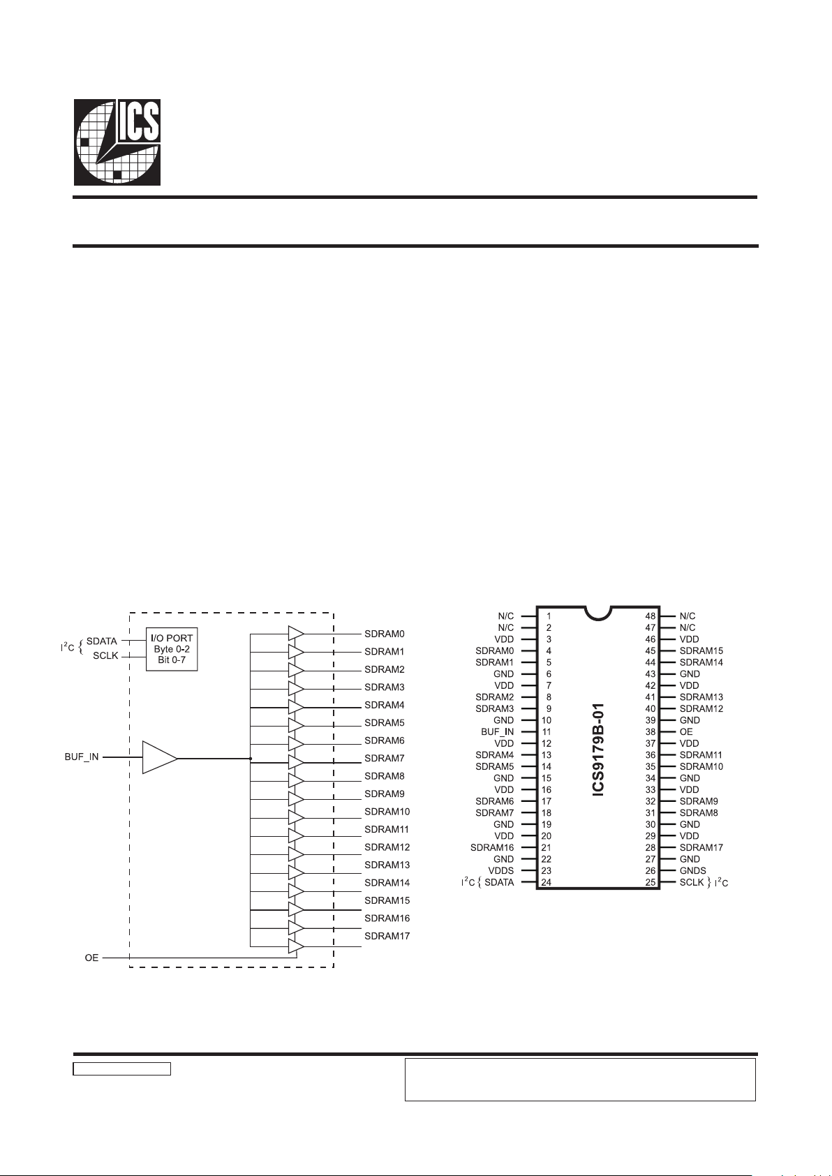
Block Diagram
PentiumPro is a trademark of Intel Corporation
I2C is a trademark of Philips Corporation
Low Skew Buffers
9179B-01 Rev C 05/18/98
Pin Configuration
The ICS9179B-01 generates SDRAM clock buffers required
for high speed RISC or CISC microprocessor systems such as
Intel PentiumPro or Pentium II. An output enable is provided
for testability.
The device is a buffer with low output to output skew. This is
a Fanout buffer device, not using an internal PLL. This buffer
can also be a feedback to an external PLL stage for phase
synchronization to a master clock.
The individual clock outputs are addressable through I2C to
be enabled, or stopped in a low state for reduced EMI when
the lines are not needed.
High speed, low noise non-inverting (0:17) buffer for
SDRAM clock buffer applications.
Supports up to four SDRAM DIMMS
Synchronous clocks skew matched to 250ps window on
SDRAM.
I
2
C Serial Configuration interface to allow individual
clocks to be stopped.
Multiple VDD, VSS pins for noise reduction
Tri-state pin for testing
Custom configurations available
3.0V 3.7V supply range
48-pin SSOP package
48-Pin SSOP
ICS reserves the right to make changes in the device data identified in this
publication without further notice. ICS advises its customers to obtain the latest
version of all device data to verify that any information being relied upon by the
customer is current and accurate.
Page 2
2
ICS9179B-01
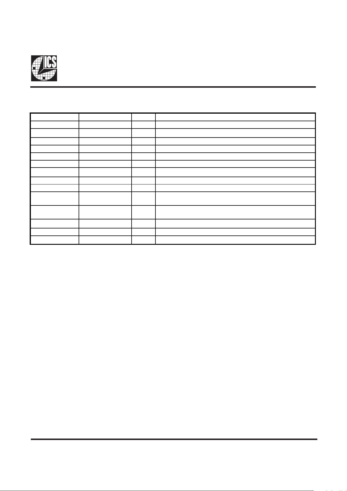
Pin Descriptions
Power Groups
VDD = Power supply for SDRAM buffer
VDDS = Power supply for I2C circuitry
PIN NUMBER PIN NAME TYPE DESCRIPTION
4, 5, 8, 9 SDRAM (0:3) OUT SDRAM Byte 0 clock outputs
1
13, 14, 17, 18 SDR AM (4:7) O UT SDRAM B yte 1 cloc k outpu ts
1
31, 32, 35, 36 SDRAM ( 8:11) OU T SDRAM Byte 2 clock outputs
1
40, 41, 44, 45 SDRAM (12:15) OUT SDRAM Byte 3 clock outputs
1
21, 28 SDRAM (16:17) OUT SDRAM clock outputs useable for feedback.
1
11 BUF_IN IN Input for buffers
38 OE IN Tri-states all outputs when held LOW. Has internal pull-up.
2
24 SDATA I /O Data pin for I2C circuitry
3
25 SCLK I/O Clock pin for I2C circuitry
3
3, 7, 12, 16, 20,
29, 33, 37, 42, 46
VDD PWR 3.3V Power supply for SDRAM buffer
6, 10, 15, 19, 22,
27, 30, 34, 39, 43
GND PW R Ground for SDRAM buffer
23 VDDS PWR 3.3V Power supply for I
2
C circuitry
26 GNDS PWR Ground for I
2
C circuitry
1, 2, 47, 48 N/C - Pins are not internally connected
Notes:
1. At power up all eighteen SDRAM outputs are enabled and active.
2. OE has a 100K Ohm internal pull-up resistor to keep all outputs active.
3. The SDATA and SCLK inputs both also have internal pull-up resistors with values above 100K Ohms as well for
complete platform flexibility.
Ground Groups
GND = Ground for SDRAM buffer
GNDS = Ground for I2C circuitry
Page 3

3
ICS9179B-01
VDD
This is the power supply to the internal core logic of the
device as well as the clock output buffers for SDRAM(0:17).
This pin operates at 3.3V volts. Clocks from the listed buffers
that it supplies will have a voltage swing from Ground to this
level. For the actual guaranteed high and low voltage levels
for the Clocks, please consult the DC parameter table in this
data sheet.
GND
This is the power supply ground (common or negative) return
pin for the internal core logic and all the output buffers.
SDRAM(0:17)
These Output Clocks are use to drive Dynamic RAMs and
are low skew copies of the CPU Clocks. The voltage swing of
the SDRAMs output is controlled by the supply voltage
that is applied to VDD of the device, operates at 3.3 volts.
I2C
The SDATA and SCLOCK Inputs are use to program the
device. The clock generator is a slave-receiver device in the
I2C protocol. It will allow read-back of the registers. See
configuration map for register functions. The I2C
specification in Philips I2C Peripherals Data Handbook (1996)
should be followed.
BUF_IN
Input for Fanout buffers (SDRAM 0:17).
OE
OE tristates all outputs when held low.
VDDS
This is the power supply to I2C circuitry.
GNDS
This is the ground to I2C circuitry.
Technical Pin Function Descriptions
Page 4

4
ICS9179B-01
Serial Configuration Command Bitmaps
Byte 0: SDRAM Clock Register
A. For the clock generator to be addressed by an I2C controller, the following address must be sent as a start sequence, with
an acknowledge bit between each byte.
B. The clock generator is a slave/receiver I2C component. It can "read back "(in Philips I2C protocol) the data stored in the
latches for verification. (set R/W# to 1 above). There is no BYTE count supported, so it does not meet the Intel SMB
PIIX4 protocol.
C. The data transfer rate supported by this clock generator is 100K bits/sec (standard mode)
D. The input is operating at 3.3V logic levels.
E. The data byte format is 8 bit bytes.
F. To simplify the clock generator I2C interface, the protocol is set to use only block writes from the controller. The bytes
must be accessed in sequential order from lowest to highest byte with the ability to stop after any complete byte has
been transferred. The Command code and Byte count shown above must be sent, but the data is ignored for those two
bytes. The data is loaded until a Stop sequence is issued.
G. In the power down mode (PWR_DWN# Low), the SDATA and SCLK pins are tristated and the internal data latches
maintain all prior programming information.
H. At power-on, all registers are set to a default condition. Bytes 0 through 2 default to a 1 (Enabled output state).
General I2C serial interface information
Notes: 1 = Enabled; 0 = Disabled, outputs held low
Then Byte 0, 1, 2, etc in
sequence until STOP.
Clock Generator
Address (7 bits)
ACK
+ 8 bits dummy
command code
ACK
+ 8 bits dummy
Byte count
ACK
A(6:0) & R/W#
D2
(H)
BIT PIN# PWD DESCRIPTION
Bit7 18 1 SDRAM7 (Act/Inact)
Bit6 17 1 SDRAM6 (Act/Inact)
Bit5
14 1
SDRAM5 (Act/Inact)
Bit4 13 1
SDRAM4 (Act/Inact)
Bit3
91
SDRAM3 (Act/Inact)
Bit2 8 1
SDRAM2 (Act/Inact)
Bit1 5 1 SDRAM1 (Act/Inact)
Bit0 4 1 SDRAM0 (Act/Inact)
Byte 0, 1, 2, etc in sequence until STOP.
Clock Generator
Address (7 bits)
ACK
Byte 0 ACK Byte 1 ACK
A(6:0) & R/W#
D3
(H)
Note: PWD = Power-Up Default
Page 5

5
ICS9179B-01
Byte 1: SDRAM Clock Register
Functionality
Notes: 1 = Enabled; 0 = Disabled, outputs held low
Byte 2: PCICLK Clock Register
Notes: 1 = Enabled; 0 = Disabled, outputs held low
BIT PIN# P WD DESCRIPTION
Bit 7 28 1 SDRA M17 (Act/Inact)
Bit 6 21 1 SDRA M16 (Act/Inact)
Bit 5 - 1 Reserved
Bit 4 - 1 Reserved
Bit 3 - 1 Reserved
Bit 2 - 1 Reserved
Bit 1 - 1 Reserved
Bit 0 - 1 Reserved
OE# SDRAM (0:3) SDRAM (4:7) SDRAM (8:11) SDRAM (12:15) SDRAM (16:17)
0 Hi-Z Hi-Z Hi-Z Hi-Z Hi-Z
1 1 X BUF_IN 1 X BUF_IN 1 X BUF_IN 1 X BUF_IN 1 X BUF_IN
BIT PIN# PWD DESCRIPTION
Bit 7 45 1 SDRAM15 (Act/Inact)
Bit 6 44 1 SDRAM14 (Act/Inact)
Bit 5 41 1 SDRAM13 (Act/Inact)
Bit 4 40 1 SDRAM12 (Act/Inact)
Bit 3 36 1 SDRAM11 (Act/Inact))
Bit 2 35 1 SDRAM10 (Act/Inact)
Bit 1 32 1 SDRAM9 (Act/Inact)
Bit 0 31 1 SDRAM8 (Act/Inact))
ICS9179B-01 Power Management
The values below are estimates of target specifications.
Condition
Max 3.3V supply consumption
Max discrete cap loads
VDD = 3.465V
All static inputs = VDD or GND
No Clock Mode
(BUF_IN - VDD1 or GND)
I
2
C Circuitry Active
3mA
Active 66MHz
(BUF_IN = 66.66MHz)
115mA
Active 100MHz
(BUF_IN = 100.00MHz)
180mA
Note: PWD = Power-Up Default
Page 6

6
ICS9179B-01
Absolute Maximum Ratings
Supply Voltage. . . . . . . . . . . . . . . . . . . . . . . . . . . 7.0 V
Logic Inputs . . . . . . . . . . . . . . . . . . . . . . . . . . . . GND 0.5 V to VDD +0.5 V
Ambient Operating Temperature . . . . . . . . . . . . 0°C to +70°C
Storage Temperature . . . . . . . . . . . . . . . . . . . . . . 65°C to +150°C
Stresses above those listed under Absolute Maximum Ratings may cause permanent damage to the device. These ratings are
stress specifications only and functional operation of the device at these or any other conditions above those listed in the
operational sections of the specifications is not implied. Exposure to absolute maximum rating conditions for extended periods
may affect product reliability.
Electric al Characterist ics - Input & Supply
TA = 0 - 70C; Supply Voltage VDD = 3.3 V + / -5% (unl ess otherwise stated)
PARAMETER
SY MBOL CONDITIONS MIN TY P MAX UNITS
Inpu t High Voltage
V
IH
2V
DD
+0.3 V
In put Low Vol t age
V
IL
VSS-0.3 0.8 V
Input High Current
I
IH
VIN = V
DD
5uA
I
IL
VIN = 0 V; Inputs wi th no pull -up resistors - 5 uA
I
IL
VIN = 0 V; In put s with 100K pull-up resistors -60 - 33 uA
I
DD1
CL = 0 pF; FIN @ 66M 80 120 mA
I
DD2
CL = 0 pF; FIN @ 100M 120 180 mA
I
DD3
CL = 30 pF; RS=33Ω; FIN @ 66M 180 260 mA
I
DD4
CL = 30 pF; RS=33Ω; FIN @ 100M 240 360 mA
I
DD5
Sto pped, input at 0 or VD D 500 µA
Inpu t frequenc y
F
i
1
VDD = 3.3 V; All Outputs Loaded 10 150 MHz
Input Capacitance
C
IN
1
Logic Inputs 5 pF
1
Guarant e ed by design, n ot 100% tested in production.
Input Low Current
O pe rat ing Supply
Current
Page 7

7
ICS9179B-01
Ele ctrical Characteristic s - SDRAM
TA = 0 - 70C; VDD = V
DDL
= 3.3 V +/-5%; CL = 20 - 30 pF (unless otherwise stated)
PARAMETER SYMBOL CONDITIONS MIN TYP MAX UNITS
O utp ut Impedance R
DSP
VO = VDD*(0.5) 10 24
Ω
O utp ut Impedance R
DSN
VO = VDD*(0.5) 10 24
Ω
O utput High Volta ge V
OH
IOH = -36 mA 2.4 3 V
Output Low Voltage V
OL
IOL = 23 mA 0.27 0.4 V
Ou tput High Curre nt I
OH
VOH = 2.0 V -115 -54 mA
Output Low Current I
OL
VOL = 0.8 V 40 57 mA
Rise Time
1
T
r
VOL = 0.4 V, VOH = 2.4 V 0.95 1.33 ns
Fall Time
1
T
f
VOH = 2.4 V , VOL = 0.4 V 0.95 1.33 ns
Duty Cycle
1
D
t
VT = 1.5 V 45 51 55 %
Skew
1
T
sk
VT = 1.5 V 110 250 ps
T
PROP
VT = 1.5 V 1 5 6 ns
Propagation
1
T
PROPENVT
= 1.5 V 1 8 ns
T
PROPDISVT
= 1.5 V
18ns
1
Guarenteed by design, no t 100% tested in production.
Page 8

8
ICS9179B-01
General Layout Precautions:
1) Use a ground plane on the top layer
of the PCB in all areas not used by
traces.
2) Make all power traces and vias as
wide as possible to lower
inductance.
Notes:
1 All clock outputs should have series
terminating resistor. Not shown in all
places to improve readibility of
diagram
2 Optional EMI capacitor should be
used on all CPU, SDRAM, and PCI
outputs.
Capacitor Values:
All unmarked capacitors are 0.01µF ceramic
Page 9

9
ICS9179B-01
SSOP Package
Ordering Information
ICS9179BF-01
Pattern Number (2 or 3 digit number for parts with ROM code patterns)
Package Type
F=SSOP
Device Type (consists of 3 or 4 digit numbers)
Prefix
ICS, AV = Standard Device
Example:
ICS XXXX F - PPP
SYMBOL C OMMON DIMENSIONS VARIATIONS D N
MIN. NOM . MAX. MIN. NOM. MAX.
A .095 .101 .110 AC .620 .625 .630 48
A1 .008 .012 .016
A2 .088 .090 .092
B .008 .010 .0135
C.005- .010
D See Variations
E . 292 .296 .299
e0.025 BSC
H .400 .406 .410
h .010 .013 .016
L .024 .032 .040
N See Variations
∝
0° 5° 8°
X .085 .093 .100
ICS reserves the right to make changes in the device data identified in this
publication without further notice. ICS advises its customers to obtain the latest
version of all device data to verify that any information being relied upon by the
customer is current and accurate.
 Loading...