

Datasheet AV9170-05CS08, AV9170-05CN08, AV9170-04CS08, AV9170-04CN08, AV9170-02CS08 Datasheet (ICST)
...Page 1
Integrated
Circuit
Systems, Inc.
General Description Features
AV9170
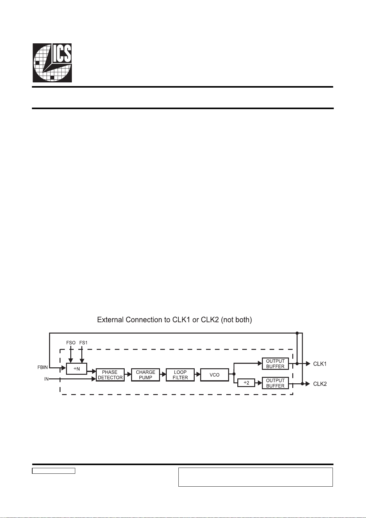
Block Diagram
Clock Synchronizer and Multiplier
AV 9170 Rev E 9/24/99
On-chip Phase-Locked Loop for clocks synchronization
Synchronizes frequencies up to 107 MHz
(output) @ 5.0V
±1ns skew (max) between input & output clocks @ 5.0V
Can recover poor duty cycle clocks
CLK1 to CLK2 skew controlled to within ±1ns @ 5.0V
3.0 - 5.5V supply range
Low power CMOS technology
Small 8-pin DIP or SOIC package
On chip loop filter
AV9170-01, -04 for output clocks 20-107 MHz @ 5.0V,
20 - 66.7 MHz @ 3.3V
AV9170-02, -05 for output clocks 5-26.75 MHz @ 5.0V,
5 - 16.7 MHz @ 3.3V
The AV9170 generates an output clock which is synchronized
to a given continuous input clock with zero delay (±1ns at 5V
VDD). Using ICSs proprietary phase-locked loop (PLL) analog CMOS technology, the AV9170 is useful for regenerating
clocks in high speed systems where skew is a major concern.
By the use of the two select pins, multiples or divisions of the
input clock can be generated with zero delay (see Tables 2 and
3). The standard versions produce two outputs, where CLK2
is always a divide by two version of CLK1.
The AV9170 is also useful to recover poor duty cycle clocks.
A 50 MHz signal with a 20/80% duty cycle, for example, can
be regenerated to the 48/52% typical of the part.
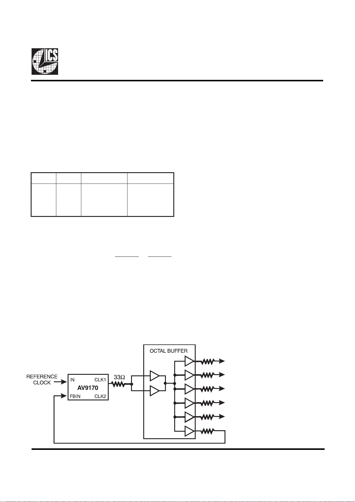
The AV9170 allows the user to control the PLL feedback,
making it possible, with an additional 74F240 octal buffer (or
other such device that offers controlled skew outputs), to
synchronize up to 8 output clocks with zero delay compared to
the input (see Figure 1). Application notes for the AV9170 are
available. Please consult ICS.
ICS reserves the right to make changes in the device data identified in this publication
without further notice. ICS advises its customers to obtain the latest version of all
device data to verify that any information being relied upon by the customer is current
and accurate.
Page 2
2
AV9170
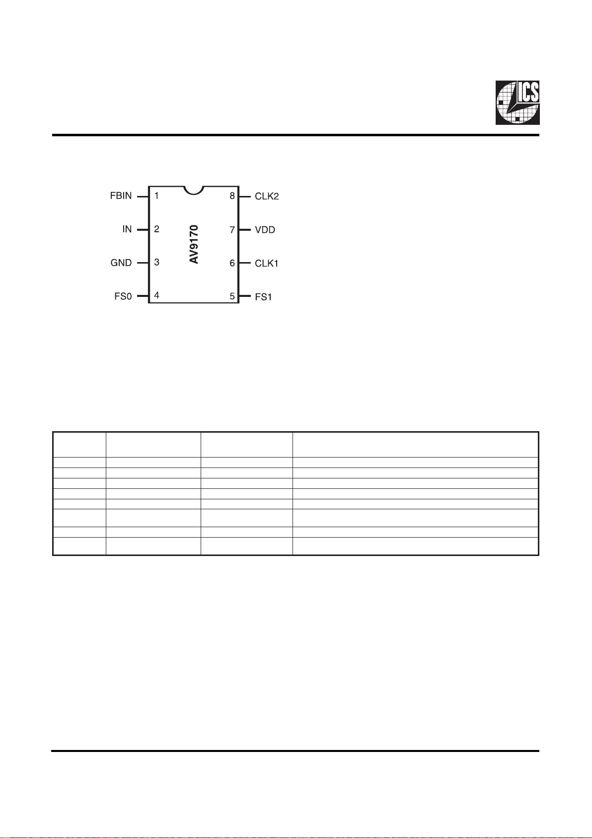
Pin Descriptions
Pin Configuration
8-Pin DIP or SOIC
NIP
-EBMUN
R
EMANNIPEPYTNOITPIRCSED
1NIBFtupnITUPNIKCABDEEF
2NItupnIkcolcecnereferrofTUPNI
3DNG—DNUORG
40SFtupnI0TCELESYCNEUQERF
51SFtupnI1TCELESYCNEUQERF
61KLCtuptuO
rof5,4,3,2,1selbaTeeS(1tuptuoKCOLC
)seulav
7DDV — ylppuSrewoP
8KLC
tuptuOrof5,4,3,2,1selbaTeeS(2tuptuoKCOLC
)seulav
Page 3
3
AV9170
The AV9170 has the following characteristics:
1. Rising edges at IN and FBIN are lined up. Falling
edges are not synchronized.
2. The relationship between the frequencies at FBIN and IN
with CLK1 feedback is shown in Table 1 below.
3. The frequency of CLK2 is half the CLK1 frequency.
4. The CLK1 frequency ranges are:
The AV9170 will only operate correctly within these
frequency ranges.
Using the AV9170
Eliminate High Speed
Clock Routing Problems
The AV9170 makes it possible to route lower speed clocks
over long distances on the PC board and to place an AV9170
next to the device requiring a higher speed clock. The
multiplied output can then be used to produce a phase locked,
higher speed output clock.
Compensate for Propagation Delays
Including an AV9170 in a timing loop allows the use of PALs,
gate arrays, etc., with loose timing specifications. The
AV9170 compensates for the delay through the PAL and
synchronizes the output to the input reference clock.
Operating Frequency Range
The AV9170 is offered in versions optimized for operation
in two frequency ranges. The -01 and -04 cover high
frequencies, 20 to 100 MHz.* The -02 and -05 operate from
5 to 25 MHz.* The AV 9 17 0 can be supplied with custom
multiplication factors and operating ranges. Consult ICS for
details.
3.3V VDD Operation
The AV9170 does operate at both 5.0V and 3.3V system
conditions. Please note the Electrical Characteristic specifications at 3.3V include a limited output frequency (66.6 MHz
max.) and a wider skew of FBIN to CLK1. For 3.3V±5%
(3.15V min.), this skew is -5.0 to 0 ns. At 3.3V±10% (3.0V
min.), the skew is widened to -8 ns to 0 ns and should be
accounted for in system design.
*At 3.3V, the maximum CLK1 frequency is 66.7 MHz for -01,
-04 and 16.7 MHz for -02, -05.
Figure 1:
Application of
AV9170 for Multiple Outputs
VDD=5V VDD=3.3V
AV9170-01, -04 20 < f
CLK1
< 107 MHz* < 66.7
AV9170-02, -05 5 < f
CLK1
< 26.75 MHz* < 16.7
1SF0SFf
NIBF
)20-,10-(f
NIBF
)50-,40-(
0
0
1
1
0
1
0
1
•2f
NI
•4f
NI
f
NI
8 • f
NI
•3f
NI
•5f
NI
•6f
NI
01 • f
NI
Functionality (Table 1:)
Page 4
4
AV9170
1SF0SF1KLC2KLC
0
0
1
1
0
1
0
1
4xNI
8xNI
2xNI
61xNI
2xNI
4xNI
NI
8xNI
1SF0SF1KLC2KLC
0
0
1
1
0
1
0
1
2xNI
4xNI
NI
8xNI
NI
2xNI
2÷NI
4xNI
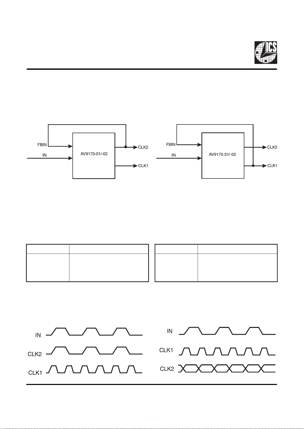
Figure 4:
Input and Output Clock Waveforms
with CLK2 Connected to FBIN
Using CLK2 Feedback
Connecting CLK2 to FBIN as shown in Figure 2 will cause all
of the rising edges to be aligned (Figure 4).
Figure 5:
Input and Output Clock Waveforms
with CLK1 Connected to FBIN
T able 2:
Functionality T able for A V9170-01, -02
with CLK2 Feedback
T able 3:
Functionality T able for A V9170-01, -02
with CLK1 Feedback
Using CLK1 Feedback
With CLK1 connected to FBIN as shown in Figure 3, the input
and CLK1 output will be aligned on the rising edge, but CLK2
can be either rising or falling (Figure 5). Consult ICS if the
CLK1 frequency is desired to be higher than 107 MHz.
For CLK2 frequencies 10 - 53.5 MHz* (-01)
For CLK2 frequencies 2.5 - 13.37 MHz (-02)
*Maximum 33.3 MHz @ 3.3V (-01), 8.33 MHz@ 3.3V (-02)
Figure 2:
For CLK1 frequencies 20 - 107 MHz (-01)
For CLK1 frequencies 5 - 26.75 MHz (-02)
Maximum 66.7 MHz @ 3.3V (-01), 16.7 MHz@ 3.3V (-02)
Figure 3:
Page 5

5
AV9170
1SF0SF1KLC2KLC
0
0
1
1
0
1
0
1
6xNI
01xNI
21xNI
02xNI
3xNI
5xNI
6xNI
01xNI
1SF0SF1KLC2KLC
0
0
1
1
0
1
0
1
3xNI
5xNI
6xNI
01xNI
5.1xNI
5.2xNI
3xNI
5xNI
Figure 8:
Input and Output Clock Waveforms
with CLK2 Connected to FBIN
Figure 9:
Input and Output Clock Waveforms
with CLK1 Connected to FBIN
T able 4:
Functionality T able for A V9170-04, -05
with CLK2 Feedback
T able 5:
Functionality T able for A V9170-04, -05
with CLK1 Feedback
Using CLK2 Feedback
Connecting CLK2 to FBIN as shown in Figure 6 will cause all
of the rising edges to be aligned (Figure 8).
Using CLK1 Feedback
With CLK1 connected to FBIN as shown in Figure 7, the
input and CLK1 output will be aligned on the rising edge, but
CLK2 can be either rising or falling (Figure 9).
For CLK2 frequencies 10 - 53 MHz* (-04)
For CLK2 frequencies 2.5 - 13.37 MHz (-05)
*Maximum 33.3 MHz @ 3.3V (-04), 8.33 MHz@ 3.3V (-05)
Figure 6:
For CLK1 frequencies 20 - 107 MHz (-04)
For CLK1 frequencies 5 - 26.75 MHz (-05)
Maximum 66.7 MHz @ 3.3V (-04), 16.7 MHz@ 3.3V (-05)
Figure 7:
Page 6

6
AV9170
Absolute Maximum Ratings
VDD (referenced to GND) . . . . . . . . . . . . . . . . 7.0 V
Operating Temperature under Bias . . . . . . . . . 0°C to +70°C
Storage Temperature . . . . . . . . . . . . . . . . . . . . 65°C to +15 0° C
Voltage on I/O pins referenced to GND . . . . . GND 0.5 V to V
DD
+ 0.5 V
Power Dissipation . . . . . . . . . . . . . . . . . . . . . . 0.5 watts
Stresses above those listed under Absolute Maximum Ratings above may cause permanent damage to the device. This is a stress
rating only and functional operation of the device at these or any other conditions above those listed in the operational sections
of the specifications is not implied. Exposure to absolute maximum rating conditions for extended periods may affect product
reliability.
*Parameter guaranteed by design and characterization. Not 100% tested in production.
Notes:
1. It may be possible to operate the AV9170 outside of these ranges. Consult ICS for your specific application.
2. All AC Specifications are measured with a 50W transmission line, load terminated with 50W to 1.4V.
3. Duty cycle measured at 1.4V.
4. Skew measured at 1.4V on rising edges. Positive sign indicates the first signal precedes the second signal.
VDD = +5V ±5%, TA = 0°C to 70°C, unless otherwise stated
Electrical Characteristics at 5V
SCITSIRETCARAHC/CD
RETEMARAPLOBMYSSNOITIDNOCTSETNIMPYTXAMSTINU
egatloVwoLtupnIVLIVDDV5= —— 8.0V
egatloVhgiHtupnIVHIVDDV5=0.2 —— V
tnerruCwoLtupnIILIVNIV0=5.1– 5–—Aµ
tnerruChgiHtupnIIHIVNIV=DD —— 5Aµ
egatloVwoLtuptuO*VLOILOAm8= —— 4.0V
egatloVhgiHtuptuO*V1HO
IHO,Am1-=
VDDV0.5=
VDDV4.- —— V
egatloVhgiHtuptuO*V2HO
IHO,Am4-=
VDDV0.5=
VDDV8.- —— V
egatloVhgiHtuptuO*V3HO
IHO,Am8-=
4.2 ——V
tnerruCylppuSI1DD
ZHM001,dedaolnU
)40-,10-(
— 0305Am
tnerruCylppuSI2DD
ZHM52,dedaolnU
)50-,20-(
— 3102Am
Page 7

7
AV9170
VDD = +5V ±5%, TA = 0°C to 70°C, unless otherwise stated
Electrical Characteristics at 5V
*Parameter guaranteed by design and characterization. Not 100% tested in production.
Notes:
1. It may be possible to operate the AV9170 outside of these ranges. Consult ICS for your specific application.
2. All AC Specifications are measured with a 50W transmission line, load terminated with 50W to 1.4V.
3. Duty cycle measured at 1.4V.
4. Skew measured at 1.4V on rising edges. Positive sign indicates the first signal precedes the second signal.
SCITSIRETCARAHCC/A
RETEMARAPLOBMYSSNOITIDNOCTSETNIMPYTXAMSTINU
emiTesiRkcolCtupnI*rKLCI —— 01sn
emiTllaFkcolCtupnI*fKLCI —— 01sn
V0.2ot8.0,emitesiRtuptuOtr*1.daolFp51 — 6.02sn
%08ot%02,emitesiRVDDtr*2.daolFp51 — 2.13sn
V8.0ot0.2,emitllaFtuptuOtf*1.daolFp51 — 4.02sn
%02ot%08,emitllaFVDDtf*2.daolFp51 — 9.02sn
10-0719VA,elcyCytuDtuptuOdt*13,2etoN.daolFp510425/8406%
20-0719VA,elcyCytuDtuptuOdt*23,2etoN.daolFp515415/9455%
amgis1,rettiJTs1* — 521003sp
etulosba,rettiJT1sba*
zHM01>1KLCroF
)40-,10-(
005–—005sp
zHM5.2>1KLCroF
)50-,20-(
etulosba,rettiJT2sba*
zHM01<1KLCroF
)40-,10-(
—— 2%
zHM5.2<1KLCroF
)50-,20-(
ycneuqerFtupnI fi1 40-,10-0719VA,1etoN8— 701zHM
ycneuqerFtupnI fi2 50-,20-0719VA2— 57.62zHM
1KLCycneuqerFtuptuO fo1 40-,10-0719VA02 — 701zHM
1KLCycneuqerFtuptuO fo2
50-,20-0719VA5— 57.62zHM
weksNIotNIBFT1weks*
daolFp51;4,2etoN
sn5<emitesirtupnI
1– 3.0– 1sn
weksNIotNIBFT2weks*
daolFp51;4,2etoN
sn01<emitesirtupnI
2– 3.0– 2sn
weks2KLCot1KLCT3weks* 4,2etoN1– 4.01sn
Page 8

8
AV9170
*Parameter guaranteed by design and characterization. Not 100% tested in production.
Notes:
1. It may be possible to operate the AV9170 outside of these ranges. Consult ICS for your specific application.
2. All AC Specifications are measured with a 50W transmission line, load terminated with 50W to 1.4V.
3. Duty cycle measured at 1.4V.
4. Skew measured at 1.4V on rising edges. Positive sign indicates the first signal precedes the second signal.
VDD = +3.3V ±5%, TA = 0°C to 70°C, unless otherwise stated
Electrical Characteristics at 3.3V
SCITSIRETCARAHC/CD
RETEMARAPLOBMYSSNOITIDNOCTSETNIMPYTXAMSTINU
egatloVwoLtupnIVLIVDDV3.3= ——2.0VDDV
egatloVhgiHtupnIVHIVDDV3.3=7.0VDD —— V
tnerruCwoLtupnIILIVNIV0=7– 4–—Aµ
tnerruChgiHtupnIIHIVNIV=DD —— 5Aµ
egatloVwoLtuptuO*VLOILOAm6= —— 4.0V
egatloVhgiHtuptuO*V1HO
IHO,Am1-=
VDDV3.3=
VDDV4.- —— V
egatloVhgiHtuptuO*V2HO
IHO,Am3-=
VDDV3.3=
VDDV8.- —— V
egatloVhgiHtuptuO*V3HO
IHO,Am6-=
4.2 —— V
tnerruCylppuSI1DD
ZHM7.66,dedaolnU
)40-,10-(
— 7103Am
tnerruCylppuSI2DD
ZHM7.61,dedaolnU
)50-,20-(
— 751Am
Page 9

9
AV9170
*Parameter guaranteed by design and characterization. Not 100% tested in production.
Notes:
1. It may be possible to operate the AV9170 outside of these ranges. Consult ICS for your specific application.
2. All AC Specifications are measured with a 50W transmission line, load terminated with 50W to 1.4V.
3. Duty cycle measured at 1.4V.
4. Skew measured at 1.4V on rising edges. Positive sign indicates the first signal precedes the second signal.
VDD = +3.3V ±5%, TA = 0°C to 70°C, unless otherwise stated
Electrical Characteristics at 3.3V
SCITSIRETCARAHCC/A
RETEMARAPLOBMYSSNOITIDNOCTSETNIMPYTXAMSTINU
emiTesiRkcolCtupnI*rKLCI —— 01sn
emiTllaFkcolCtupnI*fKLCI —— 01sn
V0.2ot8.0,emitesiRtuptuOtr*1.daolFp51 — 1.12sn
%08ot%02,emitesiRVDDtr*2.daolFp51 — 8.14sn
V8.0ot0.2,emitllaFtuptuOtf*1.daolFp51 — 8.02sn
%02ot%08,emitllaFVDDtf*2.daolFp51 — 2.13sn
40-,10-0719VA,elcyCytuDtuptuOdt*13,2etoN.daolFp51042506%
50-,20-0719VA,elcyCytuDtuptuOdt*23,2etoN.daolFp51541555%
amgis1,rettiJTs1* — 051003sp
etulosba,rettiJT1sba*
zHM01>1KLCroF
)40-,10-(
005–—005sp
zHM5.2>1KLCroF
)50-,20-(
etulosba,rettiJT2sba*
zHM01<1KLCroF
)40-,10-(
2–—2%
zHM5.2<1KLCroF
)50-,20-(
ycneuqerFtupnI fi1 40-,10-0719VA7— 7.66zHM
ycneuqerFtupnI fi2 50-,20-0719VA2— 7.61zHM
1KLCycneuqerFtuptuO fo1 40-,10-0719VA02 — 7.66zHM
1KLCycneuqerFtuptuO fo2
50-,20-0719VA5— 7.61zHM
weksNIotNIBFT1weks*
daolFp51;4,2etoN
0.3£VDD
£
7.3
0.8– 0.2– 0sn
weksNIotNIBFT2weks*
daolFp51;4,2etoN
0.3£VDD
£
7.3
0.5– 0.2– 0sn
weks2KLCot1KLCT3weks* daolFp51;4,2etoN0.2– 9.0– 0sn
Page 10

10
AV9170
General Layout Precautions:
1) Use a ground plane on the top layer
of the PCB in all areas not used by
traces.
2) Make all power traces and vias as
wide as possible to lower
inductance.
Notes:
1) All clock outputs should have series
terminating resistor. Not shown in all
places to improve readibility of
diagram.
Connections to VDD:
Page 11

11
AV9170
Ordering Information
AV9170-xxCN8 (8 Lead Plastic DIP [300 mils])
A V9170-xxCS8 (8 Lead SOIC [150 mils])
8-Pin DIP PACKAGE
8-Pin SOIC P ACKAGE
For the SOIC package, the AV9170-01 is marked AV70-1 and the AV9170-02 is marked AV70-2.
ICS XXXX-PPP M X#W
Lead Count & Package Width
Lead Count = 1, 2 or 3 digits
W = 0.3" SOIC or 0.6" DIP; None = Standard Width
Package Type
N = DIP (Plastic)
S = SOIC
Pattern Number (2 or 3 digit number for parts with ROM code patterns)
Device Type (consists of 3 or 4 digit numbers)
Prefix
ICS = Standard Device; AV = ICS (West Coast)
Example:
ICS reserves the right to make changes in the device data identified in this publication
without further notice. ICS advises its customers to obtain the latest version of all
device data to verify that any information being relied upon by the customer is current
and accurate.
 Loading...