

Page 1
Integrated
Circuit
Systems, Inc.
General Description
Features
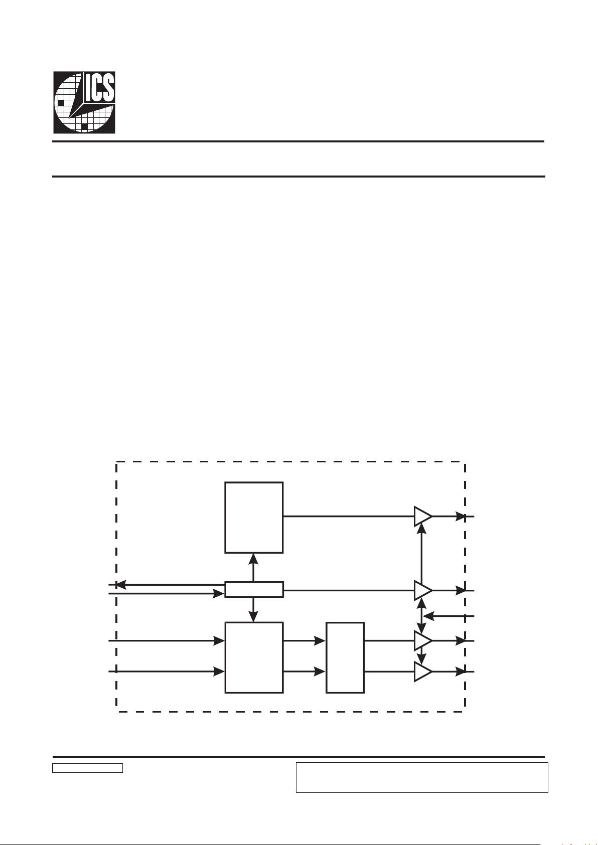
XTAL OSC
BCLK(0:5)
PCLK(0:3)
OEN
REF(0:2)
48 MHz
SYNC
REG
PLL
CLOCK
GEN
PLL
CLOCK
GEN
X2
X1
FS0
FS1
Block Diagram
Pentium is a trademark of Intel Corporation
PowerPC is a trademark of Motorola Corporation
Frequency Generator and Integrated Buffers for Intel Pentium
and Pentium ProTM
µµ
µµ
µP's
ICS9169-01
The ICS9169-01 generates all clocks required for high speed
RISC or CISC microprocessor systems such as 486, Pentium/
Pentium Pro™, PowerPC™, etc. Four different reference
frequency multiplying factors are externally selectable with
smooth frequency transitions. These multiplying factors can
be customized for specific applications. A test mode is provided
to drive all clocks directly.
High drive BCLK outputs typically provide greater than 1V/
ns slew rate into 30pF loads. PCLK outputs typically provide
better than 1V/ns slew rate into 20pF loads while maintaining
50±5% duty cycle. The REF clock outputs typically provide
better than 0.5V/ns slew rates.
• Generates four processor, six bus, three 14.318 MHz
and one 48 MHz clock for ISA bus, audio, super I/O
and bus bridge devices
• Supports the Intel MARS chip set
• Synchronous clocks skew matched to 250ps window on
PCLKs and 500ps window on BCLKs
• Test clock mode eases system design
• Selectable multiplying ratios
• Custom configurations available
• Output frequency ranges to 100 MHz (depending on
option)
• 3.0V - 5.5 V supply range
• 28-pin SOIC and 28-pin SSOP (209-mil) packages
Applications
• Ideal for high-speed RISC or CISC systems such as 486,
Pentium, Pentium Pro, PowerPC, etc.
9169-01RevE 08/28/98
ICS reserves the right to make changes in the device data identified in this publication
without further notice. ICS advises its customers to obtain the latest version of all
device data to verify that any information being relied upon by the customer is current
and accurate.
Page 2
2
ICS9169-01
Pin Configuration
Pin Descriptions
Functionality
*VCO range is limited from 60 - 200 MHz
Note 1: BCLK buffers cannot be supplied with 5 volts (pins 14 and 20) if CPU and fixed frequencies (pins 1, 8, and 26) are being
supplied with 3.3 volts
PIN NUMBER PIN NAME TYPE DESCRIPTION
2X1IN
XTAL or external referenc e frequency in put. This input in cludes XTAL load
capacitance and feedba ck bias for a 12.16 MH z crystal, nominally 14.3181 8
3 X2 OUT XTAL output which includes XTAL load capacitance.
4, 11, 23 GND PWR Ground for logic, PCLK and fixed frequency output buffers.
17
GND PW R Ground for BCL K output buffers.
1, 8, 26 VDD PW R Power for logic, PCLK an d fixed frequency output buffers.
14, 20 VDD PW R Power fo r BCLK o utput buffers.
6, 7, 9, 10 PCLK(0:3) OUT
Processor clo ck outputs w hich are a multip le of the input refere nce frequency
as shown in the table above .
13, 12 FS(0:1) IN
Frequency multiplier select pins. See table above. These inputs have internal
pull-up devices.
15, 16, 18
19, 21, 22
BCLK (0:5) OUT Bus clock outputs are fixed at 1/2 the PCLK frequency.
5 OEN IN OEN tristates all outp uts when low. This inp ut has an internal p ull-up device.
24 48MHz OUT Fixed 48 M Hz clock (with 14 .318 MHz input).
28, 27, 25 REF(0:2) OUT
REF is a b uffered copy of th e crystal oscillator o r reference input clo ck,
nominally 14.31818 M Hz.
PCLK(0:3) BCLK(0:5) 48 MHz
VCO/2 PCLK/2 48 MHz
TCLK/2 TCLK/4 TCLK/2
28 Pin SOIC
28 Pin SSOP
FS1 FS0 *VCO X1, REF
(MHz)
PCLK(0:3)
(MHz)
0 0 230/33x X1 14.31818 50 (49.7)
0 1 212/23x X1 14.31818 66 (66.5)
1 0 176/21x X1 14.31818 60 (59.9)
1 1 Test mode TCLK TCLK/2
Page 3
3
ICS9169-01
Absolute Maximum Ratings
.
Electrical Characteristics at 3.3 V
Stresses above those listed under Absolute Maximum Ratings may cause permanent damage to the device. These ratings are stess
specifications only and functional operation of the device at these or any other conditions above those listed in the operational
sections of the specifications is not implied. Exposure to absolute maximum rating conditions for extended periods may affect
product reliability.
Stresses a
stess spec
operation
periods m
Supply Voltage.................................................................................................................................................................. 7.0 V
Logic Inputs ............................................................................................................................ GND - 0.5 V to VDD + 0.5 V
Ambient Operating Temperature ........................................................................................................................... 0 t o + 7 0 C
Storage T emperature......................................................................................................................................... -65 to +150 C
VDD = 3.0 - 3.7 V, TA = 0 - 70oC unless otherwise stated
Note 1: Parameter is guaranteed by design and characterization. Not 100% tested in production.
DC Characteristics
PARAMETER SYMBOL TEST CONDITIONS MIN TYP MAX UNITS
Input Low Voltage V
IL --0.2VDD V
Input High Voltage V
IH 0.7VDD --V
Input Low Current I
IL VIN = 0 V -28.0 -10.5 -
µA
Input High Current I
IH VIN = VDD -5.0 - 5.0
µA
Output Low C urrent
1
IOL
VOL = 0.8 V;
for PCLKs & BCLKs
30.0 47. 0 - mA
Output Hi gh Curren t
1
IOH
VOL = 2.0 V; for
PCLKs & BCLKs
- -66.0 -42.0 mA
Output Low C urrent
1
IOL VOL=0.8V; for fixed CLKs 25.0 38. 0 - mA
Output Hi gh Curren t
1
IOH VOL=2.0V; for fixed CLKs - -47.0 - 30.0 mA
Output Low Vo ltage
1
VOL IOL = 15 mA; for PCLKs & BCLKs - 0.3 0.4 V
Output High Voltage
1
VOH
IOH = -30 mA;
for PCLKs & BCLKs
2.4 2.8 - V
Output Low Vo ltage
1
VOL IOL=12.5mA; for fixed CLKs - 0.3 0.4 V
Output High Voltage
1
VOH
IOH = -20mA;
for fixed CLKs
2.4 2.8 - V
Supply Current I
DD @ 66.5 MHz; all outputs unloaded - 55 110 mA
Page 4

4
ICS9169-01
Electrical Characteristics at 3.3 V
VDD = 3.0 - 3.7 V, TA = 0 - 70oC unless otherwise stated
Note 1: Parameter is guaranteed by design and characterization. Not 100% tested in production.
AC Characteristics
PARAMETER SYMBOL TES T CONDITIONS MIN TYP MAX UNITS
Rise Time
1
Tr1
20pF load, 0.8 to 2.0V
PCLK & BCLK
-0.91.5ns
Fall Time
1
Tf1
20pF load, 2.0 to 0.8V
PCLK & BCLK
-0.81.4ns
Rise Time
1
Tr2
20pF load, 20% to 80%
PCLK & BCLK
-1.52.5ns
Fall Time
1
Tf2
20pF load, 80% to 20%
PCLK & BCLK
-1.42.4ns
Duty Cyc le
1
Dt
20pF load
@ V
OUT = 1.4 V
45 50 55 %
Jitter, One Sigma
1
Tj1s1
PCLK & BCLK Clocks;
Load=20pF,
F
OUT >25 MHz
- 50 150 ps
Jitter, Absolute
1
Tjab1
PCLK & BCLK Clocks;
Load=20pF,
F
OUT
>25 MHz
-250 - 250 ps
Jitter, One Sigma
1
Tj1s2 Fixed CLK; Load=20pF - 1 3 %
Jitter, Absolute
1
Tjab2 Fixed CLK; Load=20pF -5 2 5 %
Input Frequency
1
Fj 12.0 14.318 16.0 MHz
Logic Input
Capacitance
1
CIN Logi c input pins - 5 - pF
Crystal Oscillator
Capacitance
1
CINX X1, X2 pins - 18 - pF
Power-on Time
1
ton
From VDD=1.6V to 1st
crossing of 66.5 MHz V
DD
supply ramp < 40 ms
-2.54.5ms
Frequency Settling
Time
1
ts
From 1st crossing of
acquisition to < 1% settling
-2.04.0ms
Clock Skew
Window
1
Tsk1
PCLK to PCLK;
Load=20pF; @1.4V
- 150 250 ps
Clock Skew
Window
1
Tsk2
BCLK to BCLK;
Load=20pF; @1.4V
- 300 500 ps
Clock Skew
Window
1
Tsk3
PCLK to BCLK;
Load=20pF; @1.4V
12.65ns
Page 5

5
ICS9169-01
Electrical Characteristics at 5.0 V
Note 1: Parameter is guaranteed by design and characterization. Not 100% tested in production.
VDD = 4.5 - 5.5 V, TA = 0 - 70 oC unless otherwise stated
DC Characteristics
PARAMETER SYMBOL TEST CONDITIONS MIN TYP MAX UNITS
Input Low Voltage V
IL --0.8V
Input High Voltage V
IH 2.4 - - V
Input Low Current I
IL VIN = 0 V -45 -15 -
µA
Input High Current I
IH VIN = VDD -5.0 - 5.0
µA
Output Low Current
1
IOL
VOL = 0.8 V;
for PCLKs & BCLKs
36.0 62.0 - mA
Output High Current
1
IOH
VOL = 2.0 V;
for PCLKs & BCLKs
- -152 -90.0 mA
Output Low Current
1
IOL VOL = 0.8V; for fixed CLKs 30.0 50. 0 - mA
Output High Current
1
IOH VOL=2.0V; for fixed CLKs - -110 .0 -65.0 mA
Output Lo w Voltage
1
VOL
IOL = 20 mA;
for PCLKs & BCLKs
-0.250.4V
Output High Voltage
1
VOH
IOH = -70 mA;
for PCLKs & BCLKs
2.4 4. 0 - V
Output Lo w Voltage
1
VOL IOL = 15mA; for fixed CLKs - 0.2 0.4 V
Output High Voltage
1
VOH IOH=-50mA; for fi xed CLKs 2.4 4.7 - V
Supply Current
1
IDD @ 66.5 MHz; all outputs unloaded - 80.0 160.0 mA
Page 6

6
ICS9169-01
General Layout Precautions:
1) Use a ground plane on the top layer
of the PCB in all areas not used by
traces.
2) Make all power traces and vias as
wide as possible to lower inductance.
Notes:
1) All clock outputs should have series
terminating resistor. Not shown in
all places to improve readibility of
diagram.
2) 47 ohm / 56pf RC termination should
be used at 50MHz and higher clock
loads.
3) Optional crystal load capacitors are
recommended.
Capacitor V alues:
C1, C2 : Crystal load values determined by user
C3 : 100pF ceramic
All unmarked capacitors are 0.01µF ceramic
Connections to VDD:
Page 7

7
ICS9169-01
AC Characteristics
PARAMETER SYMBOL TEST CONDITIONS MIN TYP MAX UNITS
Rise Time
1
Tr1
20pF load, 0.8 to 2.0V
PCLK & BCLK
-0.550.95ns
Fall Time
1
Tf1
20pF load, 2.0 to 0.8V
PCLK & BCLK
-0.520.90ns
Rise Time
1
Tr2
20pF load, 20% to 80%
PCLK & BCLK
-1.22.1ns
Fall Time
1
Tf2
20pF load, 80% to 20%
PCLK & BCLK
-1.12.0ns
Duty Cycle
1
Dt1 20pF load @ VOUT = 50% of VDD 45 50 55 %
Duty Cycle
1
Dt2 20pF load @ VOUT = 1.4 V 50 55 60 %
Jitter, One Sigma
1
Tj1s1
PCLK & BCLK Clocks; Load=20pF;
R=33
Ω FOUT > 25 MHz
- 50 150 ps
Jitter, Absolute
1
Tjab1
PCLK & BCLK Clocks; Load=20pF;
R=33
Ω FOUT > 25 MHz
-250 - 250 ps
Jitter, One Sigma
1
Tjis2
Fixed CLK; Load=20pF
R=33
Ω
-13%
Jitter, Absolute
1
Tjab2
Fixed CLK; Load=20pF
R=33
Ω
-5 2 5 %
Input Frequency
1
Fi 12.0 14.318 16.0 MHz
Logic Input Capacitance
1
CIN Logic input pins - 5 - pF
Crystal Oscillator
Capacitance
1
CINX X1, X2 pins - 18 - pF
Power-on Time
1
ton
From V=1.6V to 1st crossing of 66.5
MHz V
DD supply ramp < 40 ms
-2.54.5ms
Frequency Settling Time
1
ts
From 1st crossing of acquisition to
< 1% settling
-2.04.0ms
Clock Skew Window
1
Tsk1
PCLK to PCLK;
Load=20pF; @1.4V
- 150 250 ps
Clock Skew Window
1
Tsk2
BCLK to BCLK;
Load=20pF; @1.4V
- 300 500 ps
Clock Skew Window
1
Tsk3
PCLK to BCLK;
Load=20pF; @1.4V
12.65 ns
Electrical Characteristics at 5.0 V
VDD = 4.5 - 5.5 V, TA = 0 - 70 oC unless otherwise stated
Note 1: Parameter is guaranteed by design and characterization. Not 100% tested in production.
Page 8

8
ICS9169-01
Ordering Information
ICS9169M-01
Example:
ICS XXXX M-PPP
Package Type
M = SOIC
Device Type (consists of 3 or 4-digit numbers)
Prefix
ICS, AV=Standard Device
Pattern Number (2 or 3-digit number for parts with ROM code pattern)
LEAD COUNT 28L
DIMENSION L 0.704
L ± 0.008
0.296 ± 0.005
0.047R
0.029 Typ.
0.018
0.406 ± 0.010
0.015
x 45˚
.0.328 ± 0.010
5˚ Typ.
5˚ Typ. ± 5
0.101
± 0.010
0.092
± 0.005
0.041
± 0.003
0.020
0.010
0.050
Pitch typ.
0.008
± 0.006
SOIC PackageSOIC Package
Pin 1Pin 1
Page 9

9
ICS9169-01
SSOP Package
A
2
C
E
SEE
DETAIL A
α
L
PARTING
LINE
DETAIL A
END VIEW
TOP VIEW
SIDE VIEW
BOTTOM VIEW
1.14
1.14
H
E/2
D/2
2.36 DIA. PIN
D
A
B
A
1
SEATING PLANE
e
C
Page 10

10
ICS9169-01
Example:
ICS XXXX M-PPP
Package Type
F=SSOP
Device Type (consists of 3 or 4-digit numbers)
Prefix
ICS, AV=Standard Device
Pattern Number (2 or 3-digit number for parts with ROM code pattern)
Ordering Information
ICS9169F-01
SYMBOL COMMON DIMENSIONS NOTE 4 6
NOTE VARIATIONS D
MIN. NOM. MAX. MIN. NOM. MAX.
A 0.68 0.73 0.78 AA 0.239 0.244 0.249 14
A 0.00 2 0.005 0.0 08 AB 0.239 0.244 0.249 16
A 0.06 6 0.068 0.0 70 AC 0.278 0.284 0.289 20
B 0 .010 0.012 0.015 AD 0.318 0.323 0. 328 24
C 0 .005 0.006 0.008 AE 0.397 0.402 0.40 7 28
D See Variations 4 A F 0.397 0.402 0.407 30
E 0.205 0.209 0.212 4
e 0.0256 BSC
H 0.301 0.307 0.311
L 0.022 0.030 0.037 5
N See Variations 6
048
Table dimensions in inches
Package dimensions - SSOP package
ICS reserves the right to make changes in the device data identified in this publication
without further notice. ICS advises its customers to obtain the latest version of all
device data to verify that any information being relied upon by the customer is current
and accurate.
 Loading...