

Page 1
Integrated
Circuit
Systems, Inc.
General Description Features
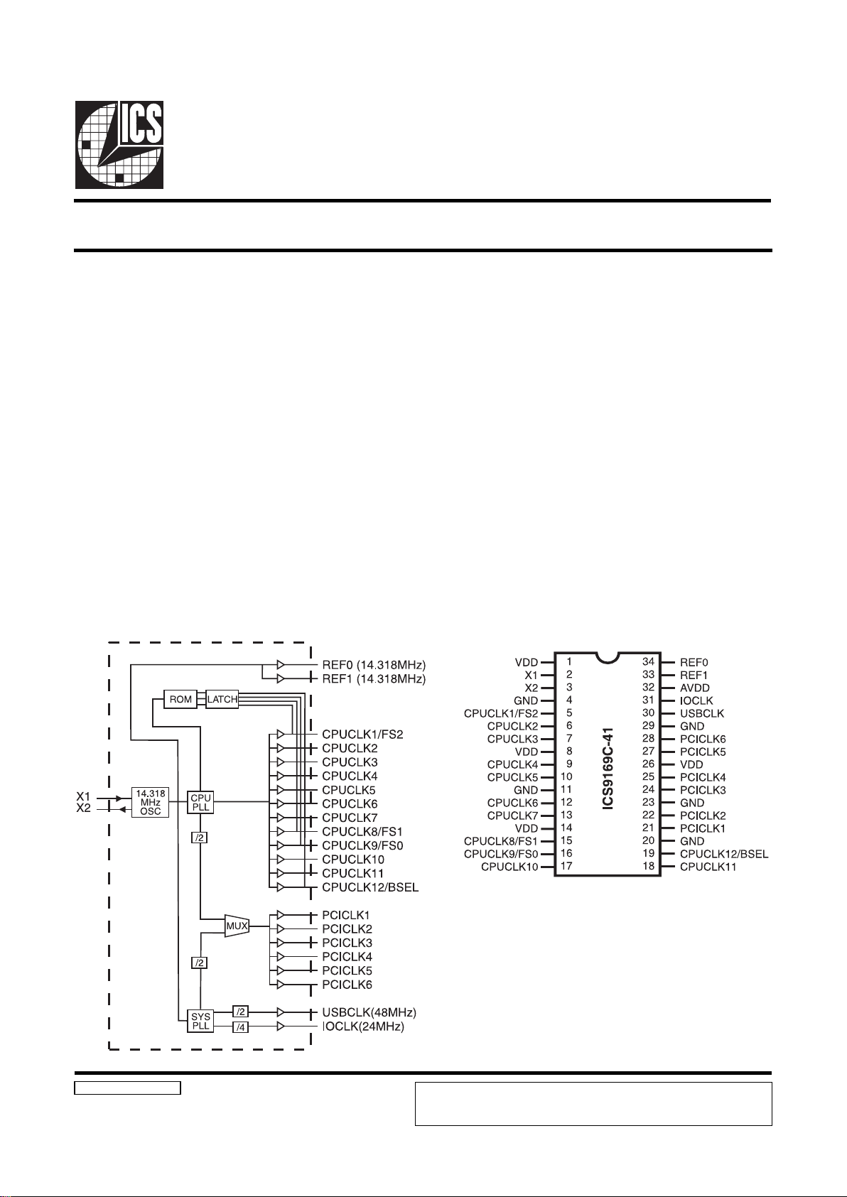
ICS9169C-41
Block Diagram
Frequency Generator for PentiumPro™ Based Systems
9169-41Rev D 5/02/00
Pin Configuration
34-Pin SSOP
Pentium is a trademark on Intel Corporation.
• 12 selectable CPU/SDRAM/AGP clocks up to 75 MHz
• Six PCI clocks, synchronous or asynchronous mode, pin
selectable by Bus Select input (pin 19)
• One USB clock at 48MHz, meets Intel jitter, accuracy, as
well as rise and fall time requirements
• One I/O clock at 24MHz
• Two Ref. Clocks at 14.318MHz
• CPU clocks to PCI clock skew of 1-4ns (CPU early)
• Low CPU and PCI clock jitter <200ps
• Low skew outputs, skew window 250ps for CPU clocks
and for PCI clocks
• Improved output drivers are designed for low EMI
• Test Mode
• 3.3V ±10% operation
• Space saving and low cost 34-pin SSOP package
The ICS9169C-41 is a Clock Synthesize/Driver chip for
Pentium, PentiumPro or Cyrix 68x86 based motherboards
using SDRAM.
Features include four dual purpose I/O pins which provide
extra CPU clocks and enable the part to be packaged in a
low-cost 34-pin SSOP package. These four pins latch the
select inputs at the internal Power-On Reset. Additionally,
the device meets the Pentium and PentiumPro power-up
stabilization, which requires that CPU and PCI clocks be
stable within 2ms after power-up.
The ICS9169C-41 clock outputs are designed for low EMI
emissions. Controlled rise and fall times, unique output
driver circuits and innovative circuit layout techniques enable
the ICS9169C-41 to have lower EMI than other clock
devices.
The ICS9169C-41 accepts a 14.318MHz reference crystal or
clock as its input and runs from a 3.3V supply.
ICS reserves the right to make changes in the device data identified in this
publication without further notice. ICS advises its customers to obtain the latest
version of all device data to verify that any information being relied upon by the
customer is current and accurate.
Page 2
2
ICS9169C-41
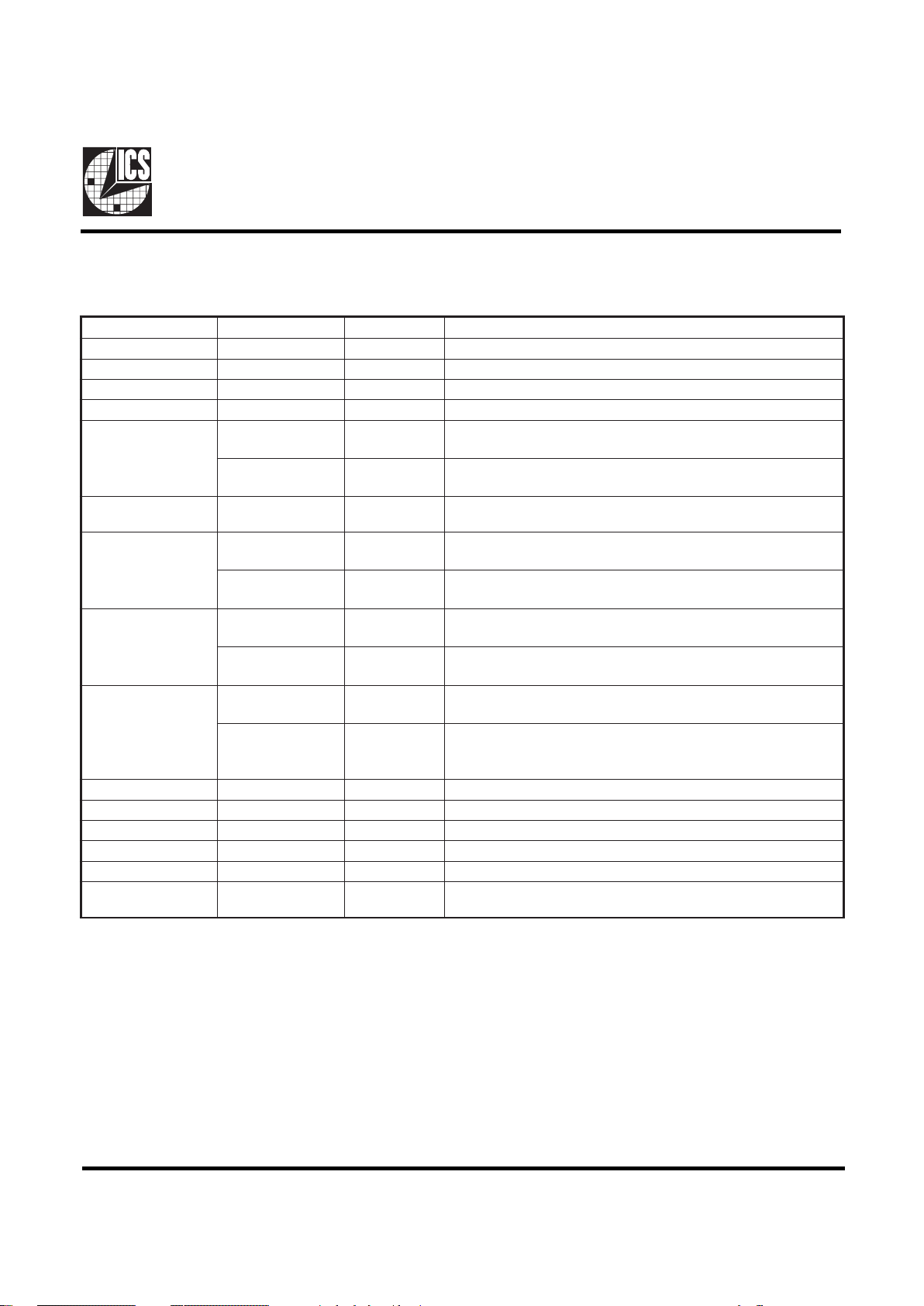
Pin Descriptions
REBMUNNIPEMANNIPEPYTNOITPIRCSED
62,41,8,1V
DD
RWPylppuSegatloV
21XNIzHM813.41yllanimoN.tupnilatsyrC
32XTUOzHM813.41yllanimoN.tuptuolatsyrC
92,32,0211,4DNGRWPdnuorG
5
1KLCUPCTUO
ecnerefertupniehtfoelpitlumaerahcihwtuptuokcolcrossecorP
.elbatgnidecerpehtninwohssakcolc
2SFNI
gnimmargorpnipderahseeS.sniptcelesreilpitlumycneuqerF
.noitanalpxerehtrufrofteehsatadsihtniretalnoitpircsed
,21,31,71,81
,6,7,9,01
)2:7,01,11(KLCUPCTUOtuptuokcolcUPC
51
8KLCUPCTUO
ecnerefertupniehtfoelpitlumaerahcihwtuptuokcolcrossecorP
.elbatgnidecerpehtninwohssakcolc
1SFNI
gnimmargorpnipderahseeS.niptcelesreilpitlumycneuqerF
.noitanalpxerehtrufrofteehsatadsihtniretalnoitpircsed
61
9KLCUPCTUO
ecnerefertupniehtfoelpitlumaerahcihwtuptuokcolcrossecorP
.elbatgnidecerpehtninwohssakcolc
0SFNI
gnimmargorpnipderahseeS.sniptcelesreilpitlumycneuqerF
.noitanalpxerehtrufrofteehsatadsihtniretalnoitpircsed
91
21KLCUPCTUO
ecnerefertupniehtfoelpitlumaerahcihwtuptuokcolcrossecorP
.elbatgnidecerpehtninwohssakcolc
LESBNI
kcolcsub)woL(suonorhcnysaro)hgiH(suonorhcnysrofnoitceleS
atadsihtniretalnoitpircsedgnimmargorpnipderahseeS.noitarepo
.noitanalpxerehtrufrofteehs
12,22,42,52,72,82)1:6(KLCICPTUO.yaledsn4-1htiwUPCotsuonorcnys.stuptuokcolCICP
03KLCBSUTUOzHM84tuptuokcolcBSU
13KLCOITUOzHM42tuptuokcolcO/I
23DDVARWPylppuSegatloVgolanA
331FERTUO)zHM813.41(tuptuokcolcecnerefeR
430FERTUO
stolsASIrof)zHM813.41(tuptuokcolcecnerefeR
Csevird(
DAOL
)Fp54=
Page 3
3
ICS9169C-41
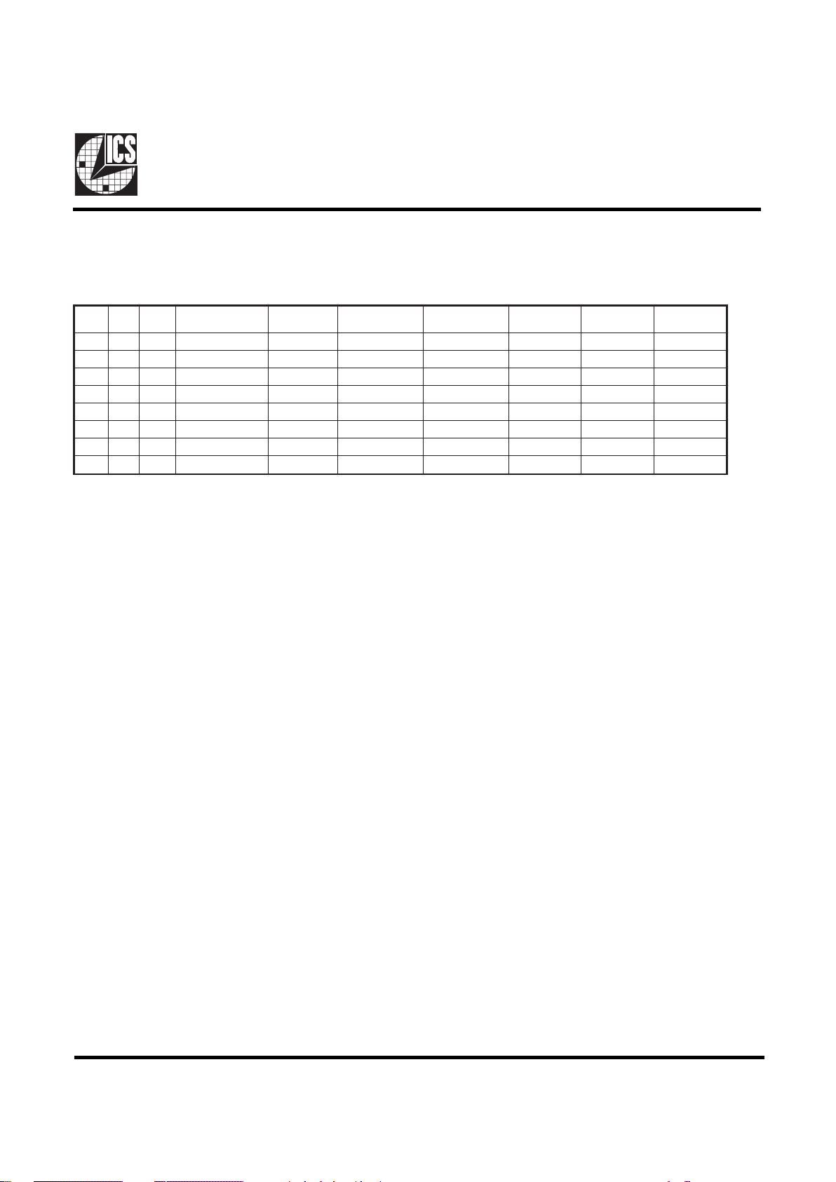
Functionality
3.3V±10%, 0-70°C
Crystal (X1, X2) = 14.31818 MHz
Notes
1. TCLK is supplied on XTALIN pin
2. Bidirectional CPUCLK I/O pins are high in test mode.
2SF1SF0SFNILATXKLCUPC
)5-1(KLCICP
1=LESB
)5-1(KLCICP
0=LESB
)1-0(FERKLCBSUKLCOI
000 zHM813.41zHM33.33zHM76.61zHM23zHM813.41zHM84zHM42
00 1 zHM813.41zHM0.57zHM5.73zHM23zHM813.41zHM84zHM42
010 zHM813.41zHM0.55zHM5.72zHM23zHM813.41zHM84zHM42
011 zHM813.41Z-IHZ-IHZ-IHZ-IHZ-IHZ-IH
10 0 zHM813.41zHM0.05zHM0.52zHM23zHM813.41zHM84zHM42
10 1 zHM813.41zHM76.66zHM33.33zHM23zHM813.41zHM84zHM42
110 zHM813.41zHM0.06zHM0.03zHM23zHM813.41zHM84zHM42
111 KLCT
)1(
2/KLCT
)2(
4/KLCT3/KLCTKLCT2/KLCT4/KLCT
Page 4

4
ICS9169C-41
Absolute Maximum Ratings
Electrical Characteristics at 3.3V
Supply Voltage . . . . . . . . . . . . . . . . . . . . . . . . . . 7.0 V
Logic Inputs . . . . . . . . . . . . . . . . . . . . . . . . . . . . GND –0.5 V to VDD +0.5 V
Ambient Operating Temperature . . . . . . . . . . . . 0°C to +70°C
Storage Temperature . . . . . . . . . . . . . . . . . . . . . . –65°C to +150°C
VDD = 3.0 – 3.7 V, TA = 0 – 70°C unless otherwise stated
Note 1: Parameter is guaranteed by design and characterization. Not 100% tested in production.
Stresses above those listed under Absolute Maximum Ratings may cause permanent damage to the device. These ratings are
stress specifications only and functional operation of the device at these or any other conditions above those listed in the
operational sections of the specifications is not implied. Exposure to absolute maximum rating conditions for extended
periods may affect product reliability.
scitsiretcarahCCD
RETEMARAPLOBMYSSNOITIDNOCTSETNIMPYTXAMSTINU
egatloVwoLtupnI
V
LI
--V2.0
DD
V
egatloVhgiHtupnI
V
HI
V7.0
DD
--V
tnerruCwoLtupnI
I
LI
V0=NIV0.82-5.01--Aµ
tnerruChgiHtupnI
I
HI
V=NIV
DD
0.5--0.5Aµ
tnerruCwoLtuptuO
1
I
LO
SKLCFER,ICP,UPCrof;V8.0=LOV0.610.52-Am
tnerruChgiHtuptuO
1
I
HO
SKLCFER,ICP,UPCrof;V0.2=LOV-0.03-0.41-Am
tnerruCwoLtuptuO
1
I
LO
KLCdexiFrof;V8.0=LOV0.910.03-Am
tnerruChgiHtuptuO
1
I
HO
KLCdexiFrof;V0.2=LOV-0.83-0.61-Am
egatloVwoLtuptuO
1
V
LO
FER,ICP,UPCrof;Am8=LOI-3.04.0V
egatloVhgiHtuptuO
1
V
HO
FER,ICP,UPCrof;Am8-=HOI4.28.2-V
egatloVwoLtuptuO
1
V
LO
s'KLCdexiF;Am81=LOI-3.04.0V
egatloVhgiHtuptuO
1
V
HO
s'KLCdexiF;Am81-=HOI4.28.2-V
tnerruCylppuS
I
DD
dedaolnustuptuolla;zHM6.66@-5759Am
Page 5

5
ICS9169C-41
Electrical Characteristics at 3.3V
VDD = 3.0 – 3.7 V, TA = 0 – 70°C unless otherwise stated
Note 1: Parameter is guaranteed by design and characterization. Not 100% tested in production.
scitsiretcarahCCA
RETEMARAPLOBMYSSNOITIDNOCTSETNIMPYTXAMSTINU
emiTesiR
1
T1rfeRtpecxEllA;V0.2ot8.0,daolFp02-9.02.1sn
emiTllaF
1
T1ffeRtpecxEllA;V8.0ot0.2,daolFp02-8.02.1sn
emiTesiR
1
T2rfeRtpecxEllAV0.2-8.0,daolFp03-3.16.1sn
emiTllaF
1
T2ffeRtpecxEllAV8.0-0.2,daolFp03-3.16.1sn
emiTesiR3rTylnofeR;V0.2-8.0;Fp54-7.10.2sn
emiTllaF3fTylnofeR;V8.0-0.2;Fp54-0.10.2sn
elcyCytuD
1
Dt V5.1=TUOV@daolFp54,03,02540555%
amgiSenO,rettiJ
1
T1s1jskcolCICP&UPC-05051sp
etulosbA,rettiJ
1
T1baj)zHM66&06@(skcolCICP&UPC052--052sp
amgiSenO,rettiJ
1
T2s1jsKLCdexiF&feR-13%
etulosbA,rettiJ
1
T2bajsKLCdexiF&feR-0.15.2%
elcyCotelcyC-rettiJTcc
stuptuOUPC-092053sp
0FER&skcolCdexiF-5.46%
ycneuqerFtupnI
1
Fi 0.21813.410.61zHM
ecnaticapaCtupnIcigoL
1
CNIsniptupnicigoL-5-Fp
rotallicsOlatsyrC
ecnaticapaC
1
CXNIsnip2X,1X-81-Fp
emiTno-rewoP
1
tno
VmorFDDzHM6.66fognissorcts1otV6.1=
VDDsm04<pmarylppus
-9.10.2sm
emiTgniltteSycneuqerF
1
ts
otnoitisiuqcafognissorcts1morF
gnilttes%1<
-0.20.4sm
wekSkcolC
1
)wodniw(T1ksV5.1@;daoLemaS;ICP-ICP&UPCotUPC-881003sp
wekSkcolC
1
)wodniw(2ksT
siUPC(V5.1@;)Fp03(ICP-)Fp02(UPC
)ylraE
0.12.10.4sn
Page 6

6
ICS9169C-41
T echnical Pin Function Descriptions
VDD
This is the power supply to the internal logic of the device as
well as the following clock output buffers:
This pin may be operated at any voltage between 3.0 and 3.7
volts. Clocks from the listed buffers that it supplies will
have a voltage swing from ground to this level. For the
actual guaranteed high and low voltage levels of these clocks,
please consult the AC parameter table in this data sheet.
GND
This is the power supply ground return pin.
X1
This pin serves one of two functions. When the device is
used with a crystal, X1 acts as the input pin for the reference
signal that comes from the discrete crystal. When the device
is driven by an external clock signal, X1 is the device input
pin for that reference clock. This pin also implements an
internal crystal loading capacitor that is connected to ground.
See the data tables for the value of the capacitor.
X2
This pin is used only when the device uses a Crystal as the
reference frequency source. In this mode of operation, X2 is
an output signal that drives (or excites) the discrete crystal.
This pin also implements an internal crystal loading capacitor
that is connected to ground. See the data tables for the value
of the capacitor.
CPU (1:12)
These pins are the clock output that drive the processor and
other CPU related circuitry that require clocks which are in
tight skew tolerance with the CPU clock. See the
Functionality table at the beginning of this data sheet for a
list of the specific frequencies that these clocks operate at
and the selection codes that are necessary to produce these
frequencies. Some of these pin serve dual functions.
PCICLK
Clock output driver for the PCI Bus.
FS0, FS1, FS2
These pins control the frequency of the clocks at the CPU,
BUS and SDRAM pins. See the Funtionality table at the
beginning of this data sheet for a list of the specific
frequencies that these clock operate at and the selection
codes that are necessary to produce these frequencies. The
device reads these pins at power-up and stores the
programmed selection code in an internal data latch. If a "1"
value is desired for a specific frequency selection bit,a 10K
ohm resistor must be connected from the appropriate FS pin
to the VDD supply. If a "O" value is desired, then the 10K
resistor must be connected to ground. After the internal
power On reset latches the input data, these pins become
output clocks and no further frequency selection is possible.
48MHz
This is a fixed frequency clock that is typically used to drive
USB peripheral device needs.
24MHz
This is a fixed frequency clock that is typically used to drive
super I/O peripheral device needs.
REF (0:1)
This is a fixed frequency clock that runs at the same frequency
as the input freerence clock (typically 14.31818 MHz) is
and typically used to drive Video and ISA BUS requirements.
Page 7

7
ICS9169C-41
Ordering Information
ICS9169CF-41
Pattern Number (2 or 3 digit number for parts with ROM code patterns)
Package Type
F=SSOP
Device Type (consists of 3 or 4 digit numbers)
Prefix
ICS, AV = Standard Device
Example:
ICS XXXX F - PPP
ICS reserves the right to make changes in the device data identified in this
publication without further notice. ICS advises its customers to obtain the latest
version of all device data to verify that any information being relied upon by the
customer is current and accurate.
 Loading...