

Page 1
Integrated
Circuit
Systems, Inc.
General Description Features
ICS9169C-40
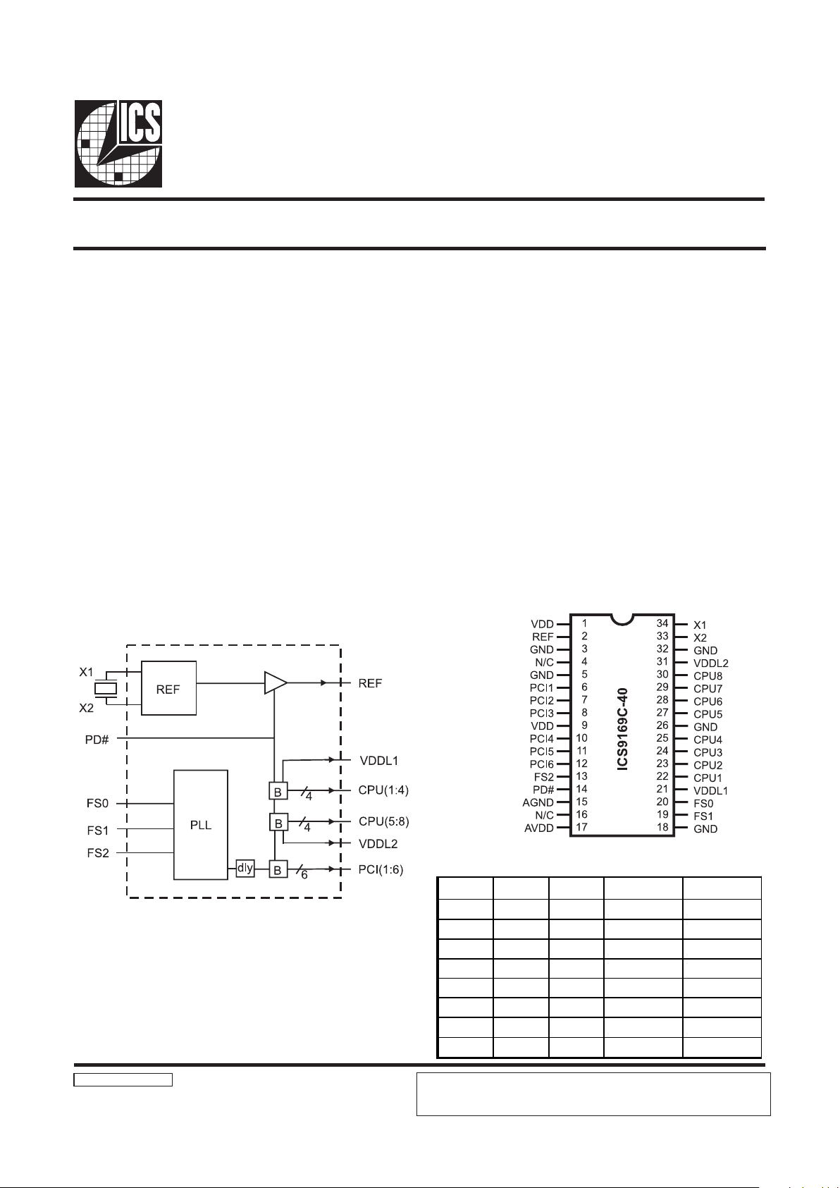
Block Diagram
System Clock Chip
9169C-40RevA072897P
Pin Configuration
34-Pin SSOP
Functionality
3.3V±10%, 0-70°C
Crystal (X1, X2) = 14.31818 MHz
Pentium is a trademark on Intel Corporation.
8 selectable CPU clocks up to 75MHz
Six synchronous PCI clocks
One Referance Clock at 14.318MHz
Power-up stabilization time = 2ms on all CPU and PCI
clocks, which meets Intel PentiumPro power-up
Low CPU and PCI clock jitter <500ps
Low skew output
Improved output drivers are designed for low EMI
Test Mode
Optional common or mixed supply mode:
(VDD = VDDL1 =VDDL2 = 3.3V)
(VDD = 3.3V, VDDL1=VDDL2 = 2.5)
(VDD = 3.3V, VDDL1 = 3.3V, VDDL2 = 2.5V)
Space saving and low cost 34-pin SSOP package
The ICS9169C-40 is a Clock Synthesizer chip for Pentium or
Cyrix CPU based motherboards using PCI.
Features include eight CPU clocks and six PCI clocks. A
Reference Output is available equal to the crystal frequency.
The device meets the Pentium power-up stabilization, which
requires that CPU and PCI clocks be stable within 2ms after
power-up.
The ICS9169C-40 clock output are designed for low EMI
emissions. Controlled rise and fall times, unique output
driver circuits and innovative circuit layout techniques enable
the ICS9169C-40 to have lower EMI than other clock
devices.
The ICS9169C-40 accepts a 14.318MHz reference crystal or
clock as its input and runs from a 3.3V supply.
FS2 FS1 FS0 CPU PCI
0 0 0 50MHz 33.3MHz
0 0 1 55MHz 36.67MHz
0 1 0 REF/2 REF/4
0 1 1 75MHz 37.5MHz
1 0 0 50MHz 25MHz
1 0 1 55MHz 27.6MHz
1 1 0 60MHz 30MHz
1 1 1 66.6MHz 33.3MHz
ICS reserves the right to make changes in the device data identified in this
publication without further notice. ICS advises its customers to obtain the latest
version of all device data to verify that any information being relied upon by the
customer is current and accurate.
Page 2
2
ICS169C-40
Pin Descriptions
PIN NUMBER PIN NAME TYPE DESCRIPTION
1, 9 VDD PWR Power supply
2 REF OUT Buffered output refe rence. 3.3V
3, 5, 18, 26, 32 GND PWR Digital Ground.
4 N/C - Not connected.
6, 7, 8, 10, 11, 12 PCI (1:6) OUT Clock output s - controlled by 3.3V V
DD
13, 19, 20 FS (0:2) IN Frequency select inputs, these inputs have internal pull-ups.
14 PD# IN
Input for tristate. If PD# = 0, then all outputs are tristated and
the device is in shutdown mode (VCO’s off, crystal oscillator
is off and all logic is reset) When PD# = 1, the device is in
normal operating mode. Has internal pull-up
15 AGND PWR Analog Ground
16 N/C - Not connected
17 AVDD PWR Analog Power Supply
21 VDDL1 PWR 3.3/2.5V Power Supply for CPU (1:4)
22, 23, 24, 25, 27, 28, 29, 30 CPU (1:8) OUT Clock outputs.
31 VDDL2 PWR 3.3/2.5V Power Supply for CPU (5:8)
33 X2 OUT Reference oscillator
34 X1 IN Re ference oscillator
Page 3

3
ICS169C-40
Absolute Maximum Ratings
Electrical Characteristics at 3.3V
Supply Voltage . . . . . . . . . . . . . . . . . . . . . . . . . . . 7.0 V
Logic Inputs . . . . . . . . . . . . . . . . . . . . . . . . . . . . GND 0.5 V to VDD +0.5 V
Ambient Operating Temperature . . . . . . . . . . . . 0°C to +70°C
Storage Temperature . . . . . . . . . . . . . . . . . . . . . . 65°C to +150°C
VDD = 3.0 3.7 V, TA = 0 70°C unless otherwise stated
Note 1: Parameter is guaranteed by design and characterization. Not 100% tested in production.
Stresses above those listed under Absolute Maximum Ratings may cause permanent damage to the device. These ratings are
stress specifications only and functional operation of the device at these or any other conditions above those listed in the
operational sections of the specifications is not implied. Exposure to absolute maximum rating conditions for extended periods
may affect product reliability.
DC Characteristics
PARAMETER SYMBOL TEST CONDITIONS MIN TYP MAX UNITS
Input Low Voltage
V
IL
- - 0.2V
DD
V
Input High Voltage
V
IH
0.7V
DD
--V
Input Low Current
I
IL
VIN=0V -50.0 25.0 50 µA
Input High Current
I
IH
VIN=V
DD
-5.0 - 5.0 µ A
Output Low Voltage
1
V
OL
IOL=12mA; for CPU, PCI - 0.3 0.4 V
Output High Voltage
1
V
OH
IOH=-12mA; for CPU, PCI 2.4 2.8 - V
Output Low Voltage
1
V
OL
IOL=7.5mA; for Ref CLK - 0.3 0.4 V
Output High Voltage
1
V
OH
IOH=-15mA; for Ref CLK 2.4 2.8 - V
Output Low Voltage
1
V
OL
IOL=7.5mA: C PU only;
VDDL (1:2) = 2.5V
-0.30.4V
Output High Voltage
1
V
OH
IOH=-13mA; CPU only;
VDDL (1:2) = 2.5V
2.0 2.2 - V
Supply Current
I
DD
@66.6 MHz; all outputs unloaded - 35 65 mA
Power Down Current I
DD
(PD)
PD#=0
All Logic Inputs to VDD
-244500µA
Other
All Logic Inputs to GND
-371700µA
Page 4

4
ICS169C-40
Electrical Characteristics at 3.3V
VDD = 3.0 3.7 V, TA = 0 70° C unless otherwise stated
Note 1: Parameter is guaranteed by design and characterization. Not 100% tested in production.
AC Characteristics
PARAMETER SYMBOL TEST CONDITIONS MIN TYP MAX UNITS
Rise Time
1
Tr1
15pF load, 0.4 t o 2.0V; VDD=VDDL
for All Outputs
-0.91.4ns
Fall Time
1
Tf1
15pF load, 2.0 t o 0.4V; VDD=VDDL
for All Outputs
- 0.8 1.2 ns
Rise Time
1
Tr2
15pF load, 0.4 t o 2.0V; VDDL=2.5V &
VDD = 2.3V; CPU
-1.52.0ns
Fall Time
1
Tf2
15pF load, 2.0 t o 0.4V; VDDL=2.5V &
VDD = 3.3V; CPU
- 1.4 2.0 ns
Duty Cycle
1
Dt
15pF load CPU, P CI, REF @
VOUT=1.5V
45 50 55 %
Duty Cycle
1
Dt
15pF load; VDDL (1:2)=2.5V
VTH=1.25V
45 49 55 %
Jitter, One Sigma
1
Tj1s1
CPU & PCI Clocks; Load=15pF,
VDD=VDDL
- 50 150 ps
Jitter, Absolute
1
Tjab1
CPU & PCI Clocks; Load=15pF,
VDD=VDDL
-220 - 220 ps
Jitter, One Sigma
1
Tj1s2 Ref; Load=15pF - 200 300 ps
Jitter, Absolute
1
Tjab2 Ref Load=15pF -500 - 500 ps
Jitter, Cycle to Cycle
(for CPU only)
T
CC
VDD=VDDL; @ 60MHz -400 - +400 ps
VDD=VDDL; @ 66MHz -350 - 350 ps
VDD=VDDL; @ 75MHz -250 - 250 ps
VDD=3.3V; VDDL=2.5;
for All Frequencies
400 - 400 ps
Input Frequency
1
Fi 12.0 14.318 1 6.0 MHz
Logic Input Capacitance
1
CIN Logic input pins - 5 - pF
Crystal Oscillator
Capacitance
1
CINX X1, X2 pins - 18 - pF
Power-on Time
1
ton
From VDD=1.6V to 1st cro ssing of 66.6
MHz VDD supply ram p < 40ms
-2.54.5 ms
Frequency Settling Time
1
ts
From 1st crossing of acquisition to <
1% settling
-1.82.0ms
Clock Skew Window
1
Tsk1
CPU to CPU & PCI to PCI; Load=15pF;
@1.5V
-250 14.5 250 ps
Clock Skew
1
Tsk2
CPU to PCI; Load=15pF; @1.5V;
VDD=VDDL; CPU is early
1.0 2.0 4.0 ns
Clock Skew
1
Tsk3
CPU to PCI; Load=15pF; (CPU is earl y)
VDDL=2.5V, VTH=1.25V;
VDD=3.3V, VTH=1.5V
0.50 1.5 3.0 ns
Page 5

5
ICS169C-40
Technical Pin Function Descriptions
VDD/AVDD
This is the power supply to the internal logic of the device as
well as the following clock output buffers:
PCI (1:6)
REF
This pin may be operated at any voltage between 3.0 and 5.5
volts. Clocks from the listed buffers that it supplies will
have a voltage swing from ground to this level. For the
actual guaranteed high and low voltage levels of these clocks,
please consult the AC parameter table in this data sheet.
GND/AGND
This is the power supply ground return pin for the chip.
XIN
This pin serves one of two functions. When the device is
used with a crystal, XIN acts as the input pin for the reference
signal that comes from the discrete crystal. When the device
is driven by an external clock signal, XIN is the device
input pin for that reference clock. This pin also implements
an internal crystal loading capacitor that is connected to
ground. See the data tables for the value of the capacitor.
XOUT
This pin is used only when the device uses a Crystal as the
reference frequency source. In this mode of operation, XOUT
is an output signal that drives (or excites) the discrete crystal.
This pin also implements an internal crystal loading capacitor
that is connected to ground. See the data tables for the value
of the capacitor.
CPU (1:8)
These pins are the clock outputs that drive processor and
other CPU related circuitry that require clocks which are in
tight skew tolerance with the CPU clock. The voltage swing
of these clocks is controlled by that which is applied to the
VDDL (1:2) pin of the device. See the Functionality table at
the beginning of this data sheet for a list of the specific
frequencies that this clock operates at and the selection
codes that are necessary to produce these frequencies.
PCI (1:6)
Outputs for PCI bus with a skew ≤ 250pS. A high current rate
of 60mA is available at 3.3V. These outputs are supplied from
VDD.
FS0, FS1, FS2
These pins control the frequency of the clocks at the CPU,
PCI pins. See the Funtionality table at the beginning of this
data sheet for a list of the specific frequencies, and the
selection codes that are necessary to produce these
frequencies. The device reads these pins at power-up. If a
"1" value is desired for a specific frequency selection bit,a
10K ohm restor must be connected from the apporapriate FS
pin to the VDD supply. If a "0" value is desired, then the 10K
resistor must be connected to ground.
REF
This is a fixed frequency clock that runs at the same frequency
as the input reference clock (typically 14.31818 MHz) is and
typically used to drive Video and ISA BUS requirements.
VDDL (1:2)
This is the power supply to the CPU clock drivers. This pin
may be operated "at any voltage" between 2.5 and 3.3 volts.
Clocks from the buffers that it supplies will have a voltage
swing form ground to this level. For the actual guaranteed
high and low voltage levels of these clocks. Please consult
the AC parameter table in this data sheet.
Page 6

6
ICS169C-40
Ordering Information
ICS9169CF-40
Pattern Number (2 or 3 digit number for parts with ROM code patterns)
Package Type
F=SSOP
Device Type (consists of 3 or 4 digit numbers)
Prefix
ICS, AV = Standard Device
Example:
ICS XXXX F - PPP
SSOP Package
SYMBOL COMMON DIMENSI ONS VARIATIONS D N
MIN. NOM. MAX. MIN. NOM. MAX.
A .097 .101 .104 AA .701 .706 .711 34
A1 .005 .009 .0115
A2 .090 .092 .094
B .014 .016 .019
C .0091 .010 .0125
D See Variations
E .292 .296 .299
e .040 BSC
H .400 .406 .410
h .010 .013 .016
L .024 .032 .040
N See Variations
∝
0° 5° 8°
X .085 .093 .100
Dimensions are in Inches
ICS reserves the right to make changes in the device data identified in this
publication without further notice. ICS advises its customers to obtain the latest
version of all device data to verify that any information being relied upon by the
customer is current and accurate.
 Loading...