

Datasheet AV9161A-01CW16, AV9161A-01CN16, ICS9161A-01CN16, ICS9161A-01CW16 Datasheet (ICST)
Page 1
Integrated
Circuit
Systems, Inc.
General Description Features
ICS9161A
9161
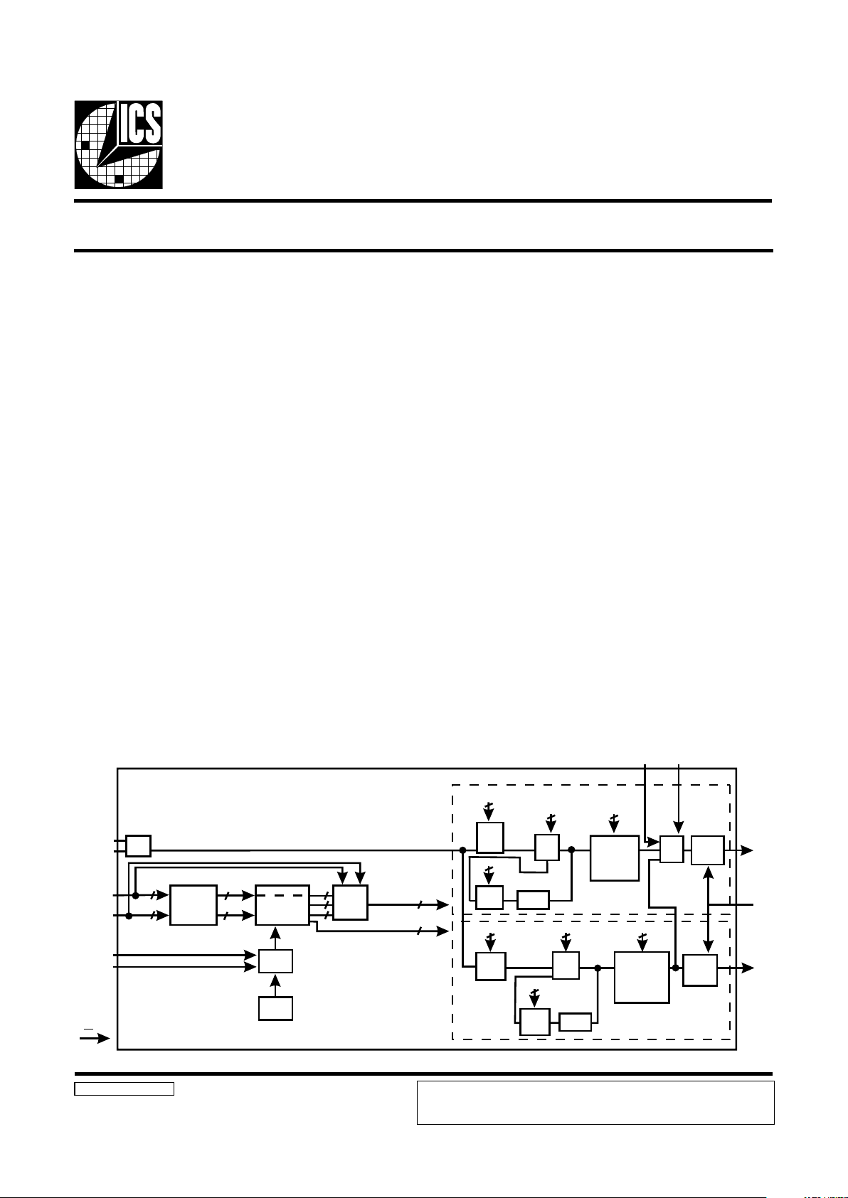
Block Diagram
Dual Programmable Graphics Frequency Generator
9161-A RevG 10/04/00
The ICS9161A is a fully programmable graphics clock
generator. It can generate user-specified clock frequencies
using an externally generated input reference or a single crystal.
The output frequency is programmed by entering a 24-bit
digital word through the serial port. Two fully userprogrammable phase-locked loops are offered in a single
package. One PLL is designed to drive the memory clock,
while the second drives the video clock. The outputs may be
changed on-the-fly to any desired frequency between 390 kHz
and 120 MHz. The ICS9161A is ideally suited for any design
where multiple or varying frequencies are required.
This part is ideal for graphics applications. It generates low
jitter, high speed pixel clocks. It can be used to replace multiple,
expensive high speed crystal oscillators. The flexibility of the
device allows it to generate non-standard graphics clocks.
The ICS9161A is also ideal in disk drives. It can generate
zone clocks for constant density recording schemes. The low
profile, 16-pin SOIC or PDIP package and low jitter outputs
are especially attractive in board space critical disk drives.
The leader in the area of multiple output clocks on a single
chip, ICS has been shipping graphics frequency generators
since October, 1990, and is constantly improving the phaselocked loop. The ICS9161A incorporates a patented fourth
generation PLL that offers the best jitter performance available.
• Pin-for-pin and function compatible with ICD2061A
• Dual programmable graphics clock generator
• Memory and video clocks are individually
programmable on-the-fly
• Ideal for designs where multiple or varying frequencies
are required
• Increased frequency resolution from optional predivide by 2 on the M counter
• Output enable feature available for tristating outputs
• Independent clock outputs range from 390 kHz to 120
MHz for VDD >4.75V
• Power-down capabilities
• Low power, high speed 0.8µ CMOS technology
• Glitch-free transitions
• Available in 16-pin, 300-mil SOIC or PDIP package
ICS reserves the right to make changes in the device data identified in this publication
without further notice. ICS advises its customers to obtain the latest version of all
device data to verify that any information being relied upon by the customer is current
and accurate.
EXTCLK EXTSEL
VCO OUTPUT
DIVIDER
R=1,2,4,8,16
32,64,128
VCO
CMOS
OUTPUT
DRIVER
MCLK
OE
VCO
DIVIDE
(N÷)
VCO OUTPUT
DIVIDER
R=1,2,4,8,16
32,64,128
VCO
REF
DIVIDE
(M÷)
MUX
CMOS
OUTPUT
DRIVER
VCLK
D14-D20
7
D0-D3
4
D11-D13
3
REF
f
D14-D20
7
D4-D10
7
D0-D3
4
D11-D13
3
24
24
MCLK
(D0-D20)
21
21
VCLK
(D0-D20)
21
21
21
REGISTERS
3
ADDRESS
INIT
ROM
POR
INIT1
INIT2
SEL0-CLK
SEL1-DATA
DECODE
LOGIC
21
DATA
CONTROL REG
XTAL
OSC
X1
X2
PD
3-TO-1
MUX
Pscale
P=2or4
REF
DIVIDE
(M÷)
D4-D10
7
VCO
DIVIDE
(N÷)
Pscale
P= 2
Page 2
2
ICS9161A
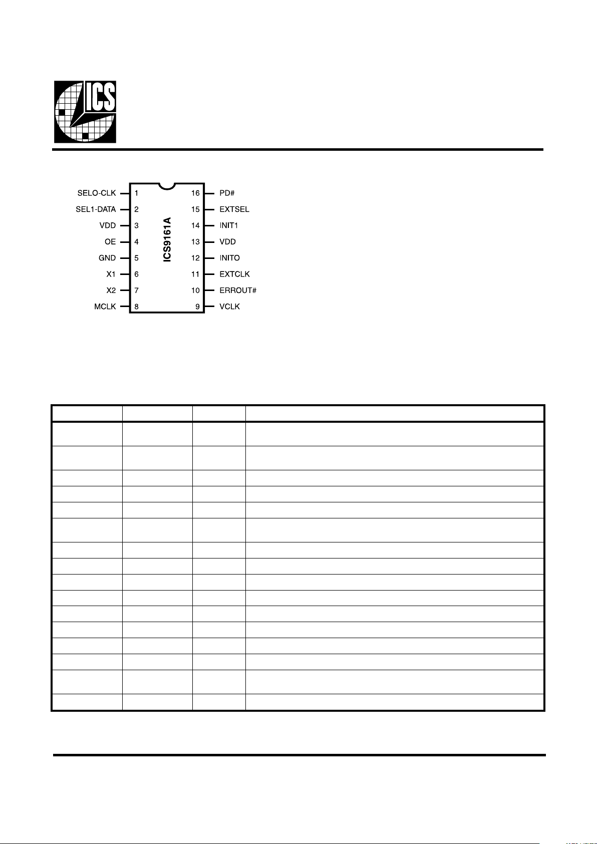
Pin Descriptions
Pin Configuration
REBMUNNIPEMANNIPEPYTNOITPIRCSED
1KLC-0LESNI
.edomgnitareponiniptceleskcolC.edomgnimmargorplairesnitupnikcolC
.DNGotnwod-lluplanretnisaH
2ATAD-1LESNI
saH.edomgnitareponiniptceleskcolC.edomgnimmargorplairesnitupniataD
.DNGotnwod-lluplanretni
3DDVARWP.rewoP
4EONI.DDVotpu-lluplanretnisaH.wolnehwstuptuosetatsirT
5DNGRWP.dnuorG
61XNI
rofsaibkcabdeefdnaecnaticapacdaolLATXsedulcnitupnisihT.tupnilatsyrC
.latsyrceht
72XTUO.ecnaticapacdaolLATXlanretnisedulcnihcihwtuptuolatsyrC
8KLCMTUO.tuptuokcolcyromeM
9KLCVTUO.tuptuokcolcoediV
01#TUORRETUO.drowdemmargorpyllairesehtnirorrenaslangiswoltuptuO
11KLCTXENI.DDVotpu-lluplanretnisaH.tupnikcolclanretxE
210TININI .DNGotnwod-lluplanretnisaH.BSL,snoitidnocpu-rewoplaitinistceleS
31DDVRWP.rewoP
411TININI .DNGotnwod-lluplanretnisaH.BSM,snoitidnocpu-rewoplaitinistceleS
51LESTXENI
otpu-lluplanretnisaH.tuptuoKLCVsa)KLCTXE(tupnikcolclanretxestceleS
.DDV
61#DPNI.DDVotpu-lluplanretnisaH.wolevitca,nipnwod-rewoP
16-Pin 300- mil SOIC or PDIP
Page 3
3
ICS9161A
Register Definitions
The register file consists of the following six registers:
Register Addressing
As seen in the VCLK Selection table, OE acts to tristate the
output. The PD# pin forces the VCLK signal high while
powering down the part. The EXTCLK pin will only be
multiplexed in when EXTSEL and SEL0 are logic 0 and SEL1
is a logic 1.
The memory clock outputs are controlled by PD# and OE
as follows:
The Clock Select pins SEL0 and SEL1 have two purposes. In
serial programming mode, these pins act as the clock and data
pins. New data bits come in on SEL1 and these bits are
clocked in by a signal on SEL0. While these pins are acquiring
new information, the VCLK signal remains unchanged. When
SEL0 and SEL1 are acting as register selects, a time-out
interval is required to determine whether the user is selecting
a new register or wants to program the part. During this initial
time-out, the VCLK signal remains at its previous frequency .
At the end of this time-out interval, a new register is selected.
A second time-out interval is required to allow the VCO to
settle to its new value. During this period of time, typically
5ms, the input reference signal is multiplexed to the VCLK
signal.
When MCLK or the active VCLK register is being reprogrammed, then the reference signal is multiplexed glitchfree to the output during the first time-out interval. A second
time-Register out interval is also required to allow the VCO
to settle. During this period, the reference signal is
multiplexed to the appropriate output signal.
The ICS9161A places the three video clock registers and the
memory clock register in a known state upon power-up. The
registers are initialized based on the state of the INIT1 and
INIT0 pins at application of power to the device. The INIT pins
must ramp up with VDD if a logical 1 on either pin is required.
These input pins are internally pulled down and will default to
a logical 0 if left unconnected.
The registers are initialized as follows:
Register Initialization
Register Selection
When the ICS9161A is operating, the video clock output is
controlled with a combination of the SEL0, SEL1, PD# and
OE pins. The video clock is also multiplexed to an external
clock (EXTCLK) which can be selected with the EXTSEL
pin. The VCLK Selection Table shows how VCLK is selected.
VCLK Selection
1TINI0TINIGERM0GER1GER2GER
0
0
1
1
0
1
0
1
005.23
000.04
053.05
446.65
571.52
571.52
000.04
000.04
223.82
223.82
223.82
053.05
223.82
223.82
223.82
053.05
EO#DPLESTXE1LES0LESKLCV
0
1
1
1
1
1
1
x
0
1
1
1
1
1
x
x
x
x
0
1
x
x
x
0
0
1
1
1
x
x
0
1
0
x
1
etatsirT
hgiHdecroF
0GER
1GER
KLCTXE
2GER
2GER
EO#DPKLCM
0
1
1
x
1
0
etatsirT
GERM
NWDRWP
MCLK Selection
sserddA
)0A-2A(
retsigeRnoitinifeD
000
100
010
110
001
011
0GER
1GER
2GER
GERM
NWDRWP
GERLTNC
1retsigeRkcolCoediV
2retsigeRkcolCoediV
3retsigeRkcolCoediV
retsigeRyromeM
edomnwod-rewoProfrosiviD
retsigeRlortnoC
Page 4
4
ICS9161A
Control Register Definitions
The control register allows the user to adjust various internal options. The register is defined as follows:
tiBemaNtiBeulaVtluafeDnoitpircseD
125C0
.tnemelpmilliwnip#DPehtedomnwod-rewophcihwsenimretedtibsihT
ehtfonoitcnufaebotslangisKLCMehtsecrof,0=5C,1edomnwod-rewoP
dnalatsyrcehtffosnrut,1=5C,2edomnwod-rewoP.retsigernwod-rewop
.stuptuollaselbasid
024C0
ycneuqerfgnirudKLCVotdexelpitlumsikcolchcihwsenimretedtibsihT
1=4C.tuptuoKLCVehtotycneuqerfecnereferehtsexelpitlum0=4C.segnahc
scihpargehterehwsnoitacilpparoftuptuoKLCVehtotKLCMsexelpitlum
fsawolssanurtonnacrellortnoc
.FER
913C0
silavretnituo-emitehT.lavretnituo-emitehtfohtgnelehtsenimretedtibsihT
,semertxeniatrecotdemmargorpsiOCVsihtfI.OCVKLCMehtmorfdevired
delbuod,1=3C.tuo-emitlamron,0=3C.trohsootebyamlavretnituo-emiteht
.lavretnituo-emit
812C0 .0ottesebtsum,devreseR
711C1
.emithgihtuptuoniesaercedsn1asesuac0=1C.elcycytudehtstsujdatibsihT
nactnemtsujdaeht,hgihsiecnaticapacdaolehtfI.tnemtsujdaonsesuac1=1C
.%05otresolcelcycytudehtgnirb
610C0 .0ottesebtsum,devreseR
512SN0
Pehtselacserp1=2SN.2ybretnuocNehtselacserp0=2SN.2retsigernostcA
.4oteulavretnuoc
411SN0
Pehtselacserp1=1SN.2ybretnuocNehtselacserp0=1SN.1retsigernostcA
.4oteulavretnuoc
310SN0
Pehtselacserp1=0SN.2ybretnuocNehtselacserp0=1SN.0retsigernostcA
.4oteulavretnuoc
Page 5
5
ICS9161A
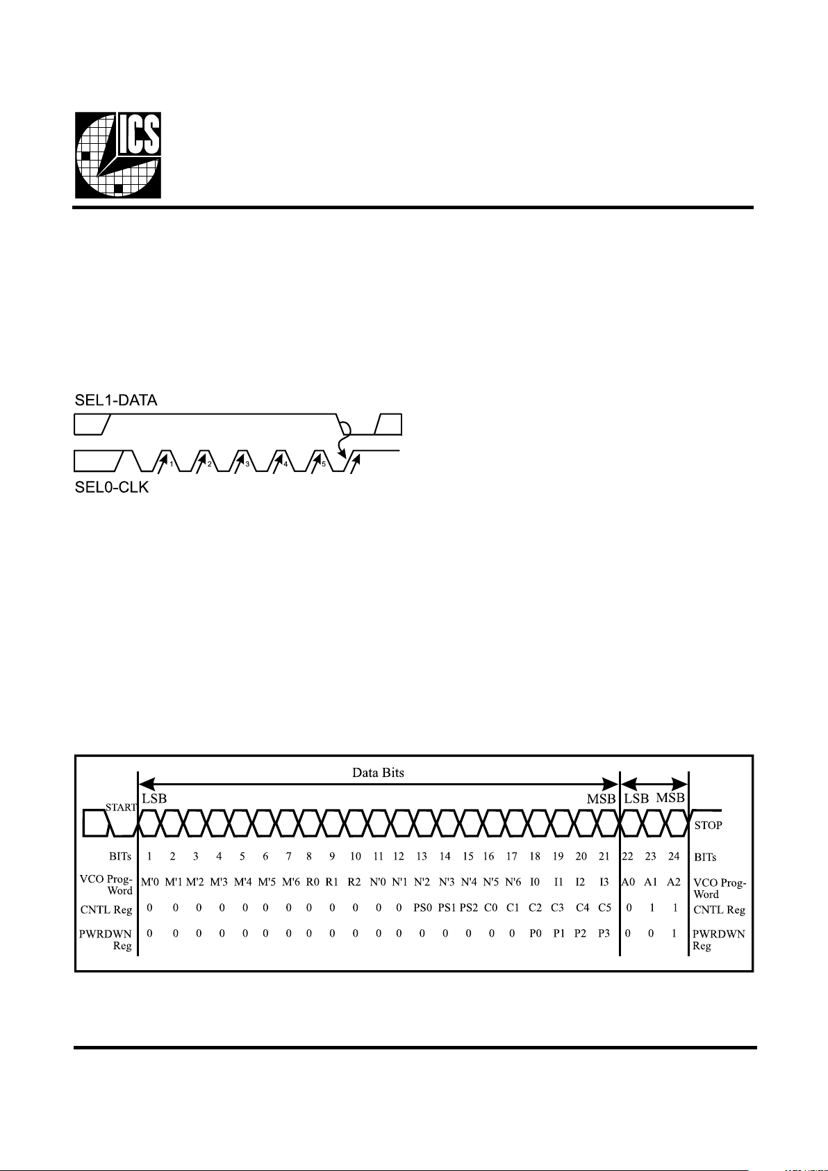
Serial Programming Architecture
The pins SEL0 and SEL1 perform the dual functions of selecting registers and serial programming. In serial programming
mode, SEL0 acts as a clock pin while SEL1 acts as the data pin.
The ICS9161A-01 may not be serially programmed when in
power-down mode.
In order to program a particular register, an unlocking sequence
must occur. The unlocking sequence is detailed in the following
timing diagram:
Serial Data Register
The serial data is clocked into the serial data register in the
order described in Figure 1 below (Serial Data Timing).
The serial data is sent as follows: An individual data bit is
sampled on the rising edge of CLK. The complement of the
data bit must be sampled on the previous falling edge of CLK.
The setup and hold time requirements must be met on both
CLK edges. For specifics on timing, see the timing diagrams
on pages 10, 11 and 12.
The bits are shifted in this order: a start bit, 21 data bits, 3
address bits (which designate the desired register), and a stop
bit. A total of 24 bits must always be loaded into the serial data
register or an error is issued. Following the entry of the last
data bit, a stop bit or load command is issued by bringing
DATA high and toggling CLK high-to-low and low-to-high.
The unlocking mechanism then resets itself following the
load. Only after a time-out period are the SEL0 and SEL1 pins
allowed to return to a register selection function.
Since the VCLK registers are selected by the SEL0 and SEL1
pins, and since any change in their state may affect the output
frequency, new data input on the selection bits is only permitted
to pass through the decode logic after the watchdog timer has
timed out. This delay of SEL0 or SEL1 data permits a serial
program cycle to occur without affecting the current register
selection.
The unlock sequence consists of at least five low-to-high
transitions of CLK while data is high, followed immediately
by a single low-to-high transition while data is low. Following
this unlock sequence, data can be loaded into the serial data
register. This programming must include the start bit, shown
in Figure 1.
Following any transition of CLK or DATA, the watchdog
timer is reset and begins counting. The watchdog timer
ensures that successive rising edges of CLK and DA T A do not
violate the time-out specification of 2ms. If a time-out
occurs, the lock mechanism is reset and the data in the serial
data register is ignored.
Figure 1: Serial Data Timing
Page 6

6
ICS9161A
The serial data register is exactly 24 bits long, enough to
accept the data being sent. The stop bit acts as a load command
that passes the contents of the Serial Data Register into the
register indicated by the three address bits. If a stop bit is not
received after the serial register is full, and more data is sent,
all data in the register is ignored and an error issued. If correct
data is received, then the unlocking mechanism re-arms, all
data in the serial data register is ignored, and an error is
issued.
ERROUT# Operation
Any error in programming the ICS9161A is signaled by
ERROUT#. When the pin goes low , an error has been detected.
It stays low until the next unlock sequence. The signal is
invoked for any of the following errors: incorrect start bit,
incorrect data encoding, incorrect length of data word, and
incorrect stop bit.
Programming the ICS9161A
The ICS9161A has a wide operating range, but it is
recommended that it is operated within the following limits:
3.15V< VDD <5.25V VDD supply voltage
1 MHz <F
REF
<60 MHz F
REF
=Input Reference
Frequency
200 kHz <F
REF/M
<5 MHz M=Reference divide 3
to 129
50 MHz < F
VCO
<120 MHz F
VCO
=VCO output
frequency
F
CLK
≤ 120 MHz F
CLK
=output frequency
The frequency of the programmable oscillator FVCO is
determined by the following fields:
The equations used to determine the oscillator frequency are:
N=N’ + 3 M=M’ + 2
F
VCO
=Prescale • N/M • F
REF
where 3 ≤ M ≤ 129 and 4 ≤ N ≤ 130
and prescale=2 or 4, as set in the control register
(Where N is the VCO divider & M is the reference divider)
The value of F
VCO
must remain between 50 MHz and 120 MHz.
As a result, for output frequencies below 50 MHz, F
VCO
must
be brought into range. To achieve this, an output divisor is
selected by setting the values of the Mux Field (R) as follows:
Where the least significant bit is the last bit of M and the most
significant bit is the first bit of I.
Output Divisor
Unlike the ICD2061A, the ICS9161A’s VCO does not
require tuning to place it in certain ranges. The ICS9161A’s
VCO will operate from 50 MHz to 120 MHz without adjusting
the VCO gain. However, to maintain compatibility, the I bits
are programmed as in the ICD2061A.
These bits are dummy bits except for the following two cases:
Index Field (I)
When the index field is set to 1111, VCLK is turned off and
both channels run from the same MCLK VCO. This is done in
an effort to reduce jitter, which may increase when VCOs run
at 2
n
multiples of one another. If the two outputs have to be
multiples of one another, it is best to mux MCLK over to the
output of the VCLK VCO and to power-down the VCLK VCO.
The multiplexed frequency will be divided down by the correct
divisor (M) and output on VCLK.
dleiFstiBfo#
)I(xednI
)'N(eulavretnuocN
)R(xuM
)'M(eulavretnuocM
4
7
3
7
RrosiviD
000
100
010
110
001
101
011
111
1
2
4
8
61
23
46
821
IFKLCV
OCV
FKLCM
OCV
0111
1111
KLCVffonruT
KCLVotKLCMxuM
zHM021-05
zHM021-05
Page 7

7
ICS9161A
Power Management Issues
Power-down mode 1
The ICS9161A contains a mechanism to reduce the quiescent
power when stand-by operation is desired. Power-down mode
1 is invoked by polling PD# low and having the proper CNTL
register bit set to zero. In this mode, VCOs are shut down, the
VCLK output is forced high, and the MCLK output is set to a
user-defined low frequency value to refresh dynamic RAM.
The power-down MCLK value is determined by the following
equation:
MCLKPD = F
REF
/(PWRDWN register divisor value)
The power-down register divisor is determined according to
the 4-bit word programmed into the PWRDWN register (see
table below).
Power-down mode 2
When there is no need for any output during power-down, an
alternate mode is available which will completely shut down
all outputs and the reference oscillator, but still preserves all
register contents. Power-down mode 2 in invoked by first
programming the power-down bit in the CNTL register and
then pulling the PD# pin low.
The PD# pin
The PD# pin has a standard internal pull-up resistor during
normal operation. When the chip goes into power-down
mode 1 or 2, the normal pull-up resistor is dynamically
switched to a weak pull-up, which reduces power consumption.
If the PD# pin is allowed to float after it has been pulled
down, the weak pull-up will bring the signal high and allow the
device to resume operation.
Po wer -Down Register Table
stibNWDRWPNWDRWPnwod-rewoPDPKLCM
3P2P1P0PeulaVretsigeRrosiviDf(
FER
)81813.41=
0
0
0
0
0
0
0
0
1
1
1
1
1
1
1
1
0
0
0
0
1
1
1
1
0
0
0
0
1
1
1
1
0
0
1
1
0
0
1
1
0
0
1
1
0
0
1
1
0
1
0
1
0
1
0
1
0
1
0
1
0
1
0
1
0
1
2
3
4
5
6
7
)tluafed(8
9
A
B
C
D
E
F
a/n
23
03
82
62
42
22
02
81
61
41
21
01
8
6
4
a/n
zHk4.744
zHk3.774
zHk4.115
zHk7.055
zHk6.695
zHk8.056
zHk9.517
zHk5.597
zHk9.498
zHM20.1
zHM91.1
zHM34.1
zHM97.1
zHM93.2
zHM85.3
Page 8

8
ICS9161A
Absolute Maximum Ratings
Note
1: Parameter is guaranteed by design and characterization. Not 100% tested in production.
VDD referenced to GND ............................................... 7V
Operating temperature under bias (T
OPER
) .................... 0°C to 70°C
Storage temperature ...................................................... -40°C to +150°C
Max. soldering temperature (10 sec) (T
SOL
) ................ +260°C
Voltage on I/O pins referenced to GND........................ GND -0.5V to VDD +0.5V
Junction temperature (Tj) .............................................. +125°C
Power dissipation ........................................................... 0.35 Watts
Stresses above those listed under Absolute Maximum Ratings may cause permanent damage to the device. This
is a stress rating only and functional operation of the device at these or any other conditions above those
indicated in the operational sections of the specifications is not implied. Exposure to absolute maximum rating
conditions for extended periods may affect product reliability.
Electrical Characteristics at 5.0V
VDD = +5V ± 5%, 0°C ≤ T
AMBIENT
≤ +70°C
scitsiretcarahCCD
RETEMARAPLOBMYSSNOITIDNOCTSETNIMPYTXAMSTINU
egatlovtupnilevelhgiHV
HI
0.2--V
egatlovtupnilevelwoLV
LI
-- 8.0V
egatlovtuptuoSOMClevelhgiH
1
V
HO
I
HO
Am4-=48.3--V
egatlovtuptuolevelwoL
1
V
LO
I
LO
Am4=--4.0V
tnerruchgihtupnII
HI
VDDV=
HI
-lluprofV52.5=
snwod
-- 001Aµ
tnerrucwoltupnII
LI
V
LI
spu-lluprofV0=052---Aµ
tnerrucegakaeltuptuOI
ZO
)etatsirt(01--01Aµ
tnerrucylppusrewoPI
DD
51-56Am
)lacipyt(tnerrucylppusrewoPI
PYT-DD
zHM06@-53-Am
tnerrucylppusrewopgolanAI
DDA
--02Am
)1edoM(tnerrucnwod-rewoPI
1DP
-6 5.7Am
)2edoM(tnerrucnwod-rewoPI
2DP
-5205Aµ
ecnaticapactupnI
1
C
NI
-- 01Fp
Page 9

9
ICS9161A
Electrical Characteristics at 5.0V (continued)
Notes:
1. Parameter guaranteed by design and characterization. Not 100% tested in production.
2. For reference frequencies other than 14.81818 MHz, the pre-loaded ROM frequencies will shift proportionally.
3. Duty cycle is measured at CMOS threshold levels. At 5 volts, VTH=2.5 volts.
4. If the interval is too short, see the time-out interval section in the control register definition.
scitsiretcarahCCA
NOITPIRCSEDEMANLOBMYSNIMPYTXAMSTINU
eulavrotallicsoecnerefeR
2
ecnerefeR
ycneuqerf
f
FER
181813.4106zHM
f/1
FER
doirepecnerefeRt
FER
6.618048.960001sn
rotallicsotupniehtrofelcycytuD
tsadenifed
1t/FER
elcycytudtupnIt1%52-%57-
seulavrotallicsotuptuO
kcolctuptuO
sdoirep
t
2
021(33.8
)zHM
-
093(4652
)zHk
sn
srotallicsotuptuoehtrofelcycytuD
3
elcycytudtuptuOt3%54-%55-
aotnisrotallicsotuptuoehtrofemitesiR
daolFp52
semitesiRt
4
--3sn
aotnisrotallicsotuptuoehtrofemitllaF
daolFp52
semitllaFt
5
--3sn
tuptuoycneuqerfdlOtuptuo1qerft
1qerf
----
tuptuoycneuqerfweNtuptuo2qerft
2qerf
----
elihwhgihsniamertuptuokcolcemiT
ycneuqerfecnereferotsexumtuptuo
f
FER
emitxumtAt5.0
FER
-t5.1
FER
sn
rofdnagnimmargorplairesroflavretnI
elttesotsegnahcOCV
4
lavretnituo-emiTt
tuo-emit
25 01sm
elihwhgihsniamertuptuokcolcemiT
eulavycneuqerfwenotsexumtuptuo
t
2qerf
emitxumtBt5.0
FER
t5.1
FER
-sn
otniogotsrotallicsotuptuoehtrofemiT
langis-SIDTUOretfaedometatsirt
noitressa
etatsirTt
6
-52-sn
revocerotsrotallicsotuptuoehtrofemiT
langis-SIDTUOretfaedometatsirtmorf
hgihseog
dilavKLCt
7
-21-sn
noitarepofoedomnwod-rewoprofemiT
tceffeekatot
nwod-rewoPt
8
-52-sn
nwod-rewopmorfyrevocerrofemiT
KLCdilavaotedom
pu-rewoPt
9
-21-sn
retfahgihogotKLCMrofemiT
hgihdetressasiNWDRWP
hgihTUOKLCMt
01
0-t
NWDRWP
sn
fotroirpKLCMfoyaleD
KLCM
talangis
tuptuo
yaledTUOKLCMt
11
t5.0
KLCM
-t5.1
KLCM
sn
kcolclairesfodoirepkcolCt
klcres
t•2
FER
-2 sm
emitpu-teSt
US
02--sn
emitdloHt
DH
01--sn
dnammocdaoLt
dmcdl
0-t
1
03+sn
Page 10

10
ICS9161A
Rise and Fall Times
Tristated Timing
Page 11

11
ICS9161A
Selection Timing
MCLK and Active VCLK Register Pr ogramming Timing
Page 12

12
ICS9161A
Soft Po wer -Do wn Timing (Mode 2)
Serial Programming Timing
Page 13

13
ICS9161A
General Layout Precautions:
1) Use a ground plane on the top layer
of the PCB in all areas not used by
traces.
2) Make all power traces and vias as
wide as possible to lower inductance.
Notes:
1) All clock outputs should ha ve series
terminating resistor. Not shown in
all places to improve readibility of
diagram.
2) 47 ohm / 56pf RC termination
should be used on all over 50MHz
outputs.
3) Optional crystal load capacitors are
recommended.
Capacitor V alues:
C1, C2 : Crystal load values determined by user
C3 : 100pF ceramic
All unmarked capacitors are 0.01µF ceramic
Connections to VDD:
Page 14

14
ICS9161A
Ordering Information
ICS9161A-01CN16
Example:
ICS XXXX - PPP M X#W
Prefix
ICS, AV=Standard Device
Device Type (consists of 3 or 4 digit numbers)
Pattern Number (2 or 3 digit number for parts with ROM code patterns, if applicable)
Package Type
N=DIP (Plastic)
Lead Count & Package Width
Lead Count=1, 2 or 3 digits
W=.3” SOIC or .6” DIP; None=Standard Width
16-Pin PDIP Packa ge
Page 15

15
ICS9161A
SOIC Packa ge (wide body)
Ordering Information
ICS9161A-01CW16
Package T ype
W=SOIC
Example:
ICS XXXX - PPP M X#W
Lead Count & Package Width
Lead Count=1, 2 or 3 digits
W=.3” SOIC or .6” DIP; None=Standard Width
Pattern Number (2 or 3 digit number for parts with ROM code patterns, if applicable)
Prefix
ICS, AV = Standard Device
Device T ype (consists of 3 or 4 digit numbers)
TNUOCDAELL61
LNOISNEMID404.0
ICS reserves the right to make changes in the device data identified in this publication
without further notice. ICS advises its customers to obtain the latest version of all
device data to verify that any information being relied upon by the customer is current
and accurate.
 Loading...