

Page 1
Integrated
Circuit
Systems, Inc.
General Description Features
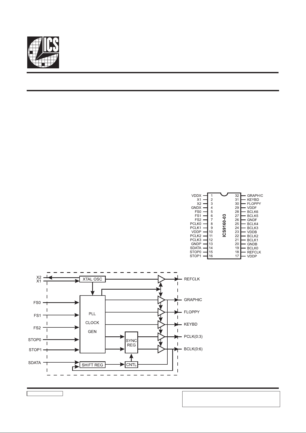
ICS9160-03
Block Diagram
Frequency Generator and Integrated Buffer for PowerPC
®
9160-03 RevC 06/19/97P
The ICS9160-03 generates all clocks required for high speed
RISC microprocessor systems based on the PowerPC 603 and
604. Five different frequency multiplying factors are selectable
and offer smooth frequency transitions. BCLK signals are
synchronous to PCLK and operate at PCLK/2 for optimum
synchronous PCI bus performance. The multiplying and ratio
factors can be customed for specific applications.
Both individual and group glitch-free stop and start ofthe
clock signals are provided, as well as a power-down mode to
mize power consumption. The individual stop and start is
provided through a serial interface control.
A global output enable pin simplifies production board testing,
and a test mode is available to aid in system design and
diagnostics.
• Generates four processor and seven synchronous
bus clocks plus graphic, floppy, keyboard and
reference clocks
• Selectable 33.3/50/60/66.6/80 MHz PCLKs
• ±150ps maximum PowerPC PLL in-band jitter
• All synchronous clocks skew matched to ±250ps
• Individual or group stop-clock control
• Power-down modes minimize standby current
• Custom configurations available
• 3.0V - 5.5 supply range
• 32-pin SOIC package
Pin Configuration
28-Pin SOIC
PRODUCT PREVIEW documents contain information on new
products in the sampling or preproduction phase of development.
Characteristic data and other specifications are subject to change
without notice.
Preliminary Product Preview
Page 2
2
ICS9160-03
Preliminary Product Preview
Pin Descriptions
* Frequencies assuming an input or crystal of 14.318 MHz.
** Device provides 18pF load capacitance for crystal.
PIN NUMBER PIN NAME TYPE DESCRIPTION
2X1IN
XTAL or external reference frequen cy input. This input includes XTAL load
capacitance and feedb ack bias for a 10-30 MH z XTAL.**
3 X2 OUT XTAL output which includes XTAL load capacitance.**
1
4
VDDX
GNDX
PWR XTAL oscillator circuit and REFCLK output power supplies.
5, 6, 7 FS(0:2) IN Frequency selection address pins. These inputs have pull-ups.
8, 9, 11, 12 PCLK(0:3) OUT
Processor clock outputs whic h are a multiple of the input reference fre quency as
shown in the table below.
10, 17
13
VDDP
GNDP
PWR
PCLK power supplies. VDDP powers the internal PCLK PLL and the
PCLK(0:3) outputs.
14 SDATA IN
Serial stop clock data is clocked in on the falling edge of BCLK. A total of 15 bits
must be clocked in using the following protocol. SDATA is sampled on the falling
edge of BCLK, so the d ata generator should chan ge data on the rising edge of
BCLK to ensure proper communication. SDATA must be low for one BCLK period
as a start bit. The next 15 rising edges of BCLK will clock data in serially. The
16th clock enables the serial da ta to take effect. Outputs associated with serial data
bits that are a one will continue without interruption. Clocks associated with serial
data bits that are a zero will be stopped in the low state g litch-free, that is, no short
clocks with the exc eption of REFCLK an d KEYBD which do not stop. This input
has an internal pull-up device.
15, 16 STOP(0:1) IN
Stop clock control pins used for glitch-free start and stop of the clock outputs as
described in the tabl e on the next page. Th ese inputs have interna l pull-up devices.
18 REFCLK OUT Buffered copy of the crystal referen ce frequency.
19, 21, 22, 24,
25, 27, 28
BCLK(0:6) OUT
Bus clock outputs havi ng selectable frequency ba sed on the FS(0:2) inputs (see
table on next page ).
20
23
GNDB
VDDB
PWR BCLK power supplies. VSSB and VDDB power BCLK(0:6).
26
29
GNDF
VDDF
PWR
Fixed clock power supplies. VSSF and VDDF power GRAPHIC, FLOPPY and
KEYBD outputs plus the fixed clock PLL.
30 FLO PPY OUT The floppy clock outpu t operates at 24 MHz..*
31 KEYBD OUT The key board clock output op erates at 12 MHz.*
32 GRAPHIC OUT The graphics system clock output operat es at 40 MHz.*
Page 3
3
ICS9160-03
Preliminary Product Preview
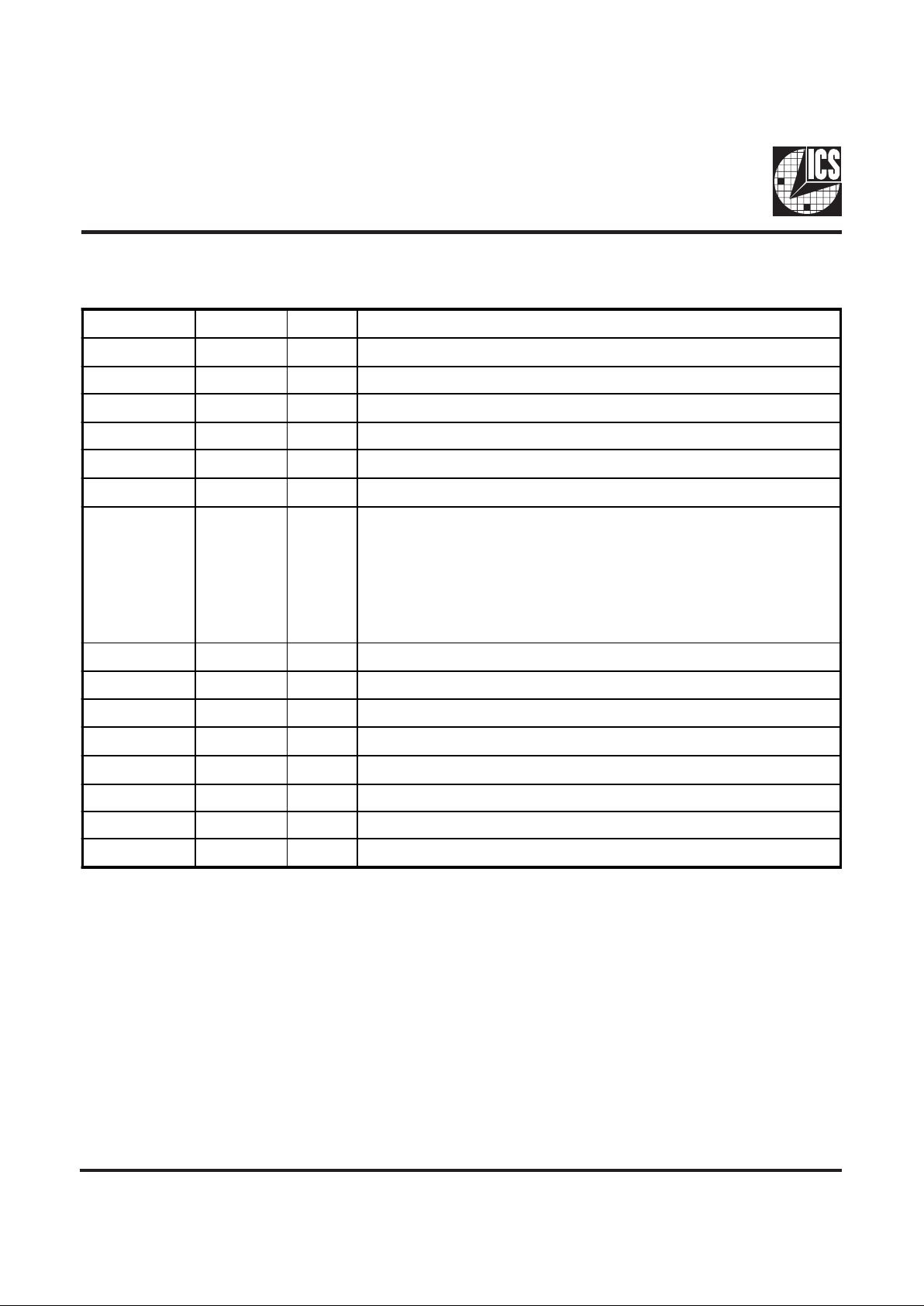
Functionality
FS2 FS1 FS0
X1, REFCLK
(MHz)
PCLK (0:3)
(MHKz)
BCLK (0:6)
(MHz)
GRAPH IC
(MHz)
FLOPPY
(MHz)
KEYBD
(MHz)
0* 0* 0* Tristate Tristate Tristate Tristate Off Tristate
0* 0* 1* H/L* Off Off H/L* H/L* H/L*
0 1 0 14.318 33.3 16.6 40.0 24.0 12.0
0 1 1 14.318 50.0 25. 0 40.0 24.0 12.0
1 0 0 14.318 60.0 30. 0 40.0 24.0 12.0
1 0 1 14.318 66.6 33. 3 40.0 24.0 12.0
1 1 0 14.318 80.0 40. 0 40.0 24.0 12.0
1 1 1 TCLK** TCLK/2 TCLK/4 TCLK/3 TCLK/5 TCLK/10
* The oscillator and all PLLs are stopped to minimize power consumption in modes ‘000’ and ‘001.’ All outputs maintain
their last stable value in mode ‘001.’ Control signals STOP0 and STOP1 can be used to ensure glitch-free start and stop
when entering mode ‘001,’ provided mode ‘001’ is entered after the clocks have stopped and exited 10ms (maximum PLL
lock time) prior to starting clocks.
** X1 is externally driven with TCLK in mode ‘111.’
Group Clock Control
STOP1+STOP0+SDA T A
*
PCLK (0:1) PCLK (2:3) BCLK (0;6)
GRAPH IC,
FLOPPY
KEYBD,
REFCLK
0 0 1 Low Low Low Low R unning
0 1 1 Low Low Running Running Run ning
1 0 1 Low Running Runnin g Running Runnin g
1 1 1 Running Running Running Running Running
Outputs stop and start glitch-free within on-clock period. Outputs will not change state if the PLLs are off.
* Each output can be stopped and started glitch-free as described in the SDATA pin description above.
+SDATA control and STOP(0:1) control are logically ORed for each individual clock.
Page 4

4
ICS9160-03
Preliminary Product Preview
Note 1: Parameter is guaranteed by design and characterization. Not 100% tested in production.
Absolute Maximum Ratings
Electrical Characteristics at 3.3V
Supply Voltage. . . . . . . . . . . . . . . . . . . . . . . . . . 7.0 V
Logic Inputs . . . . . . . . . . . . . . . . . . . . . . . . . . . . GND –0.5 V to VDD +0.5 V
Ambient Operating Temperature . . . . . . . . . . . . 0 to +70°C
Storage Temperature. . . . . . . . . . . . . . . . . . . . . . –65°C to +150°C
Stresses above those listed under Absolute Maximum Ratings may cause permanent damage to the device. This is a stress
rating only and functional operation of the device at these or any other conditions above those indicated in the operational
sections of the specifications is not implied. Exposure to absolute maximum rating conditions for extended periods may
affect product reliability.
VDD = 3.0 – 3.7 V, TA = 0 – 70°C unless otherwise stated
DC Charac teristics
PARAMETER SYMBOL TEST CONDITIONS MIN TYP MAX UNITS
Input Low Vo ltage V
IL
- - 0.2VDD V
Input High Voltage V
IH
0.7VDD - - V
Input Low Current I
IL
VIN=0V - 10.5 28.0 mA
Input High Current I
IH
VIN=V
DD
-5.0 - 5.0 mA
Output Low Current I
OL
1
VOL=0.8V;
for PCLKS & BCLKS
30.0 47.0 - m A
Output High Current I
OH
1
VOL=2.0V;
for PCLKS & BCLKS
- -66. 0 -42.0 mA
Output Low Current I
OL
1
VOL=0.8V; for fixed CLKs 25.0 38.0 - mA
Output High Current I
OH
1
VOL=2.0V; for fixed CLKs - -47.0 -30.0 mA
Output Low Voltage V
OL
IOL=15mA;
for PCLKS & BCLKS
-0.30.4V
Output High Voltage V
OH
1
IOH=-30mA;
for PCLKS & BCLKS
2.4 2.8 - V
Output Low Voltage V
OL
1
IOL=12.5mA; for fixed CLKs - 0.3 0.4 V
Output High Voltage V
OH
1
IOH=-20mA; for fixed CLKs 2.4 2.8 - V
Supply Current I
CC
@66.66 MHz; all outputs
unloaded
-60130mA
Page 5

5
ICS9160-03
Preliminary Product Preview
Note 1: Parameter is guaranteed by design and characterization. Not 100% tested in production.
Note 2: Jitter spectrum meets PowerPC PLL natural frequency in-band requirements of less than ±150ps.
Electrical Characteristics at 3.3V
VDD = 3.0 – 3.7 V
AC Chara cteristics
PARAMETER SYMBOL TEST CONDITIONS MIN TYP MAX UNITS
Rise Time T
r
1
20pF load, 0.8 to 2.0V - 1.5 3 ns
Fall Time T
f
1
20pF load, 2.0 to 0.8V - 0.9 2 ns
Rise Time T
r
1
20pF load, 20% to 80% - 2 4.5 ns
Fall Time T
f
1
20pF load, 80% to 20% - 1.8 4.25 ns
Duty Cycle D
t
1
20pF load 40 50 60 %
Jitter, One Sigma T
j1s
1
PCLK & BCLK Cloc ks; Load=20pF,
FOUT>25 MHz
-50150ps
Jitter, Absolute T
jab
1
PCLK & BCLK Cloc ks; Load=20pF,
FOUT>25 MHz
-250 - 250 ps
Jitter, One Sigma T
j1s
1
Fixed CLK and BC LK < 25 MHz and Fixed
CLK; Load=20pF
-3.0 1 3 .0 %
Jitter, Absolute T
jab
1
Fixed CLK and BC LK < 25 MHz;
Load=20pF
-5.0 2 5 .0 %
Input Frequency F
i
1
- 14.318 - MHz
Clock Skew T
sk
1
PCLK to PCLK; Load=20pF; @1.4V -250 50 250 ps
Clock Skew T
sk
1
BCLK0 to other BCLK; Load=20pF; @1.4V -500 90 500 ps
Clock Skew T
sk
1
PCLK to BCLK; Load=20pF; @1.4V 1 2.6 5 ns
Page 6

6
ICS9160-03
Preliminary Product Preview
The data is latched into the internal shift register on the falling edge of the BCLK signal with the BCLK as a reference
(see waveform above). The SDATA input pattern will change at the BCLK rising edg es and must be stable for loading into
the shift register at the BCLK falling edges.
Programming Bit Addresses
The following table lists the function of each of the 15 input programming bits for the device.
ICS9160-03 SDATA Serial Stop Clock Input Pin Bit Pattern
BIT# OUTPUT PIN
STOP CLOCK FUNCTION
(Clocks stops if Bit= Low)
0 START BIT (One "zero" bit needed to start shift register sequence.)
132GRAPHIC
2n/a
330FLOPPY
4 28 BCLK6
5 27 BCLK5
6 21 BCLK4
7 22 BCLK3
8 24 BCLK2
9 25 BCLK1
10 19 BCLK0
11 n/ a
12 12 PCLK3
13 11 PCLK2
14 9 PCLK1
15 8 PCLK0
Page 7

7
ICS9160-03
Preliminary Product Preview
32-Pin SOIC Pac ka ge
Ordering Information
ICS9160M-03
Pattern Number (2 or 3 digit number for parts with ROM code patterns)
Package Type
M=SOIC
Device Type (consists of 3 or 4 digit numbers)
Prefix
ICS, AV = Standard Device
Example:
ICS XXXX M - PPP
LEAD COUNT 32L
DIMENSONL .804
PRODUCT PREVIEW documents contain information on new
products in the sampling or preproduction phase of development.
Characteristic data and other specifications are subject to change
without notice.
 Loading...