

Page 1
Integrated
Circuit
Systems, Inc.
General Description
Features
ICS9159C-02
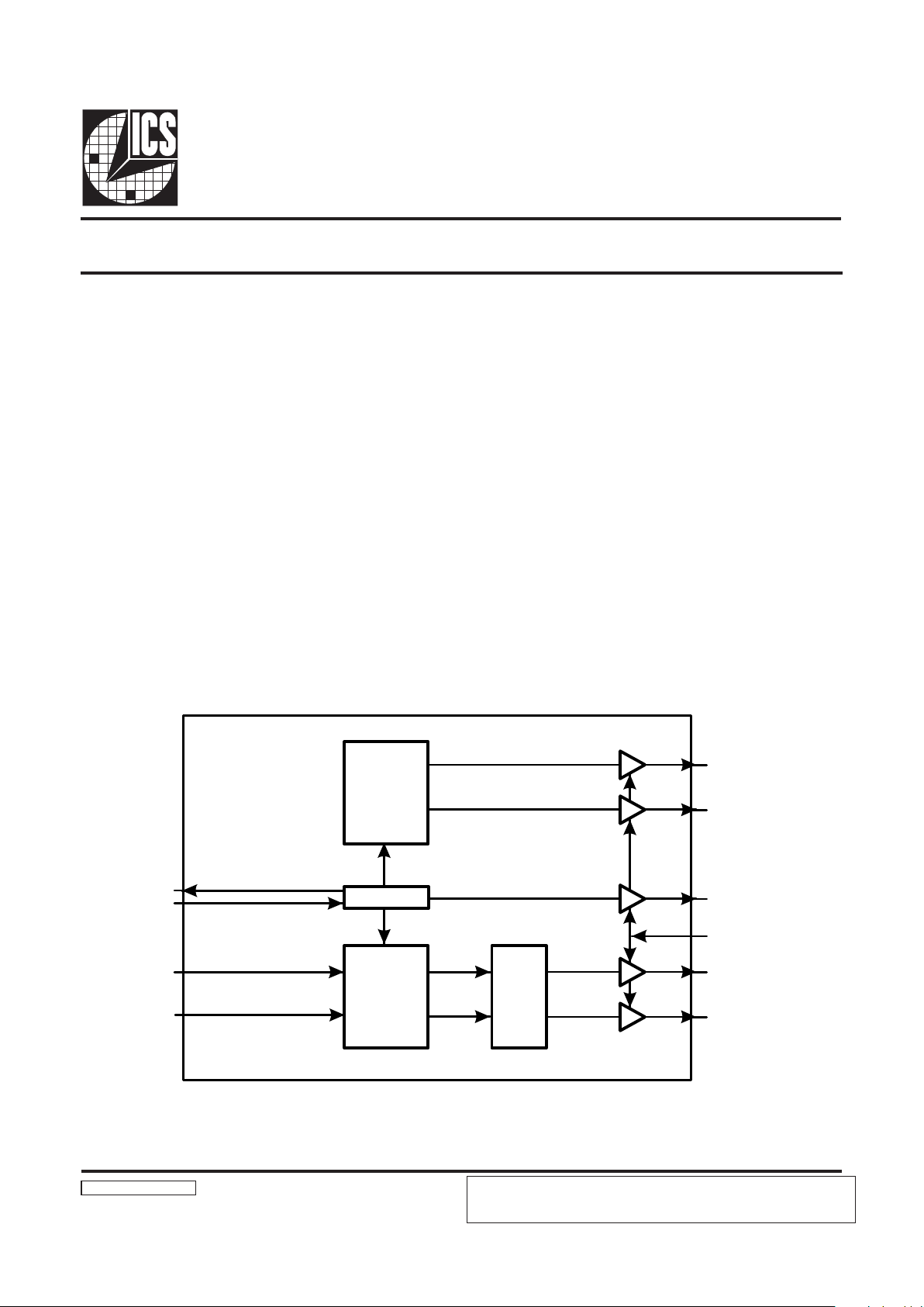
The ICS9159C-02 generates all clocks required for high
speed RISC or CISC microprocessor systems such as 486,
Pentium, PowerPC, etc. Four different reference frequency
multiplying factors are externally selectable with smooth
frequency transitions. These multiplying factors can be
customized for specific applications. A test mode is provided
to drive all clocks directly.
High drive BCLK outputs provide typically greater than
1V/ns slew rate into 30pF loads. PCLK outputs provide
typically better than 1V/ns slew rate into 20pF loads while
maintaining +/−5% duty cycle.
Generates up to four processor and six bus clocks, plus
disk, keyboard and reference clocks
Synchronous clocks skew matched to 250ps window on
PCLKs and 500ps window on BCLKs
Test clock mode eases system design
Custom configurations available:
Output frequency ranges to 100 MHz on options
Selectable multiplying and processor/bus ratios
Stop clock control stops clock glitch-free; available as
mask option
3.0V - 5.5V supply range
28-pin SOIC package
Applications
Ideal for high-speed RISC or CISC systems such as
486, Pentium, PowerPC, etc.
XTAL OSC
BCLK(0:5)
PCLK(0:3)
OEN
REF(0:1)
KEYBD
DISK
SYNC
REG
PLL
CLOCK
GEN
PLL
CLOCK
GEN
X2
X1
FS0
FS1
9159-02 Rev D 062397
Block Diagram
Pentium is a trademark of Intel Corporation
PowerPC is a trademark of Motorola Corporation
Frequency Generator and Integrated Buffer for PENTIUM
TM
ICS reserves the right to make changes in the device data identified in this publication
without further notice. ICS advises its customers to obtain the latest version of all
device data to verify that any information being relied upon by the customer is current
and accurate.
Page 2
2
ICS9159C-02
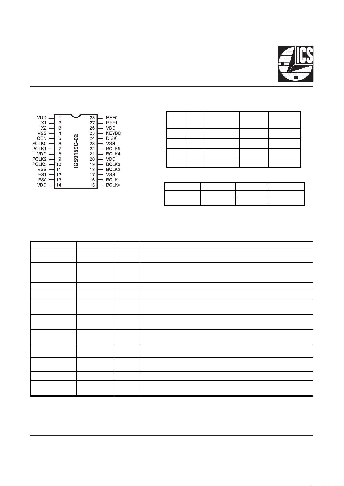
Pin Configuration
Pin Descriptions
Functionality
*VCO range is limited from 60 - 200 MHz
PCLK(0,3) BCLK(0,5) DISK KEYBD
VCO/2 PCLK/2 24 MHz 12 MHz
TCLK/2 TCLK/4 TCLK/4 TCLK/8
PIN NUMBER PIN NAME TYPE DESCRIPTION
1, 8, 14,
20, 26
VDD PWR Power for logic, PCLK and fixe d frequency output buf fers.
2X1IN
XTAL or external refer ence frequency input . This input i ncludes
XTAL load capacitance and feedback bias for a 1 2 - 16 MHz
crystal, no minally 14.31818 MHz.
3 X2 OUT XTAL output which incl udes XTAL load capacitance.
4, 11, 17, 23 VSS PWR Ground for logic, PCLK and fixed f requency output buf fers.
6, 7, 9, 10 PCLK(0:3) OUT
Processor clock outputs which are a mul tiple of the in put reference
frequency as shown in the table above.
13, 12 FS(0:1) IN
Frequency multipl ier select pins. See table above. These inputs have
internal pul l-up devices.
15, 16, 18 19,
21, 22
BCLK(0:5) OUT Bus clock output s are fixed at one ha lf the PCLK frequency.
5OENIN
OEN tristates al l outputs when l ow. This input has an i nternal pullup device.
24 DISK OUT
The DISK controller clock is fixed at 24 MHz
(with 14.318 MHz inpu t).
25 KEYBD OUT The KEYBD clock is fixed at 12 MHz (with 14.318 MHz input ).
28, 27 REF(0:1) OUT
REF is a buffered cop y of the crystal oscillator or r eference input
clock nominally 14.31818 MHz.
Note: BCLK buffers cannot be supplied with 5 volts (pins 14 and 20) if CPU and fixed frequencies (pins 1, 8, and 26) are being
supplied with 3.3 volts
28-Pin SOIC
FS1 FS0 *VCO
X1, REF
(MHz)
CPU
(MHz)
0 0 118/17xX1 14.318 50(49.7)
0 1 65/7xX1 14.318 66.6(66.5)
1 0 92/11xX1 14.318 60(59.9)
1 1 Test mode TCLK TCLK/2
Page 3
3
ICS9159C-02
Absolute Maximum Ratings
Electrical Characteristics at 3.3 V
Stresses above those listed under Absolute Maximum Ratings may cause permanent damage to the device. These ratings are
stess specifications only and functional operation of the device at these or any other conditions above those listed in the
operational sections of the specifications is not implied. Exposure to absolute maximum rating conditions for extended periods
may affect product reliability.
Supply Voltage ......................................................................................... 7.0 V
Logic Inputs ..................................................... GND - 0.5 V to VDD + 0.5 V
Ambient .................................................... Operating Temperature0 to +70 C
Storage Temperature .................................................................. 65 to +150 C
VDD = 3.0 - 3.7 V, TA = 0 - 70oC unless otherwise stated
Note 1: Parameter is guaranteed by design and characterization. Not 100% tested in production.
DC Characteristics
PARAMETER SYMBOL TEST CONDITIONS MIN TYP MAX UNITS
Input Low Volta ge V
IL - -0.2VDD V
Input High Volt age V
IH 0.7VDD - - V
Input Low Current I
IL VIN=0V -28.0 -1 0.5 - mA
Input High Curre nt I
IH VIN=VDD -5.0 - 5.0 mA
Output Low Current
1
IOL VOL=0.8V for PCLKS & BCLKS 30.0 47.0 - mA
Output High Curre nt
1
IOH VOL=2.0V for PCLKS & BCLKS - -66. 0 -42.0 mA
Output Low Current
1
IOL VOL=0.8V for fixed CLKs 25.0 38.0 - mA
Output High Curre nt
1
IOH VOL=2.0V for fi xed CLKs - -47.0 -30.0 mA
Output Low Voltage
1
VOL IOL=15mA for PCLKS & BCLKS - 0.3 0.4 V
Output High
Voltage
1
VOH IOH=-30mA for PCLKS & BCLKS 2.4 2.8 - V
Output Low Voltage
1
VOL IOL=12.5mA for fixed CLKs - 0.3 0.4 V
Output High
Voltage
1
VOH IOH=-20mA for fix ed CLKs 2.4 2.8 - V
Supply Curren t I
DD @66.5 MHz all outputs unloaded - 55 110 mA
Page 4

4
ICS9159C-02
Electrical Characteristics at 3.3 V
VDD = 3.0 - 3.7 V, TA = 0 - 70oC unless otherwise stated
Note 1: Parameter is guaranteed by design and characterization. Not 100% tested in production.
AC Characterist ics
PARAMETER S YMBOL TES T CONDITI ONS MIN TYP MAX UNITS
Ris e Time
1
Tr1
20pF load, 0.8 t o 2.0V
PCLK & BCLK
- 0.9 1. 5 ns
Fall Time
1
Tf1
20pF load, 2.0 t o 0.8V
PCLK & BCLK
- 0.8 1. 4 ns
Ris e Time
1
Tr2
20pF load, 20% to 80%
PCLK & BCLK
- 1.5 2. 5 ns
Fall Time
1
Tf2
20pF load, 80% to 20%
PCLK & BCLK
- 1.4 2. 4 ns
Duty Cycl e
1
Dt 20pF load @ VOUT=1 .4V 45 50 55 %
Jitter, One Sigma
1
Tj1s1
PCLK & BCLK Cl ock s;
Load=20pF, FOUT>25 MHz
- 50 150 ps
Jitter, Absolute
1
Tjab1
PCLK & BCLK Cl ock s;
Load=20pF, FOUT >25 MHz
-250 - 250 ps
Jitter, One Sigma
1
Tj1s2 Fi xed CLK; Load=20pF - 1 3 %
Jitter, Absolute
1
Tjab2 Fi xed CLK; Load=20pF -5 2 5 %
Input Frequency
1
Fi 12.0 14.318 16.0 MHz
Logic Input
Capacitance
1
CIN Logic input pins - 5 - pF
Crystal Oscillator
1
Capacitance1
C
INX X1, X2 pins - 18 - pF
Power-on Time
1
ton
From VDD=1.6V to 1st
crossing of 66.5 MHz V
DD
supply ramp<40ms
- 2.5 4. 5 ms
Frequency Settling
Time
1
ts
From 1st crossi ng of
acquisition to <1% settling
- 2.0 4. 0 ms
Clock Skew
Window
1
Tsk1
PCLK to PCLK;
Load=20pF; @1.4V
- 150 250 ps
Clock Skew
Window
T
sk2
BCLK to BCLK;
Load=20pF; @1.4V
- 300 500 ps
Clock Skew
Window
1
Tsk3
PCLK to BCLK;
Load=20pF; @1.4V
1 2.6 5 ns
Page 5

5
ICS9159C-02
Electrical Characteristics at 5.0 V
Note 1: Parameter is guaranteed by design and characterization. Not 100% tested in production.
DC C haracteristics
PARAMETER SYMBOL TEST CONDITIONS MIN TYP M AX UNITS
Input L ow Vo ltage V
IL - - 0.8 V
Input High Voltage V
IH 2.4 - - V
Input Low Current I
IL V IN=0V -45 -15 - mA
Input High Current I
IH VIN =VDD -5.0 - 5.0 mA
Output L ow Current
1
IOL VOL=0.8V ; for PCLKS & BCLK S 3 6.0 62.0 - m A
Output High Current
1
IOH VOH=2.0V ; for PC LKS & BCL KS - -152 - 90.0 mA
Output L ow Current
1
IOL VOL=0.8V; for fixed CL Ks 30.0 50.0 - m A
Output High Current
1
IOH VOL=2.0V; for fixed CLKs - -110.0 -65.0 mA
Outp ut Low V oltage
1
VOL IOL=20mA; for P CLKS & BCLKS - 0.25 0.4 V
Outp ut High V oltage
1
VOH IOH=-70mA; for PCL KS & BCLKS 2.4 4.0 - V
Outp ut Low V oltage
1
VOL IOL=15mA; for fixed CLKs - 0.2 0.4 V
Outp ut High V oltage
1
VOH IOH=-50mA; for fixed CLKs 2.4 4.7 - V
Supply Current I
DD @66.5 MHz; all outputs unloaded - 80.0 160.0 mA
VDD = 4.5 - 5.5 V, TA = 0 - 70oC unless otherwise stated
Page 6

6
ICS9159C-02
Electrical Characteristics at 5.0 V
VDD = 4.5 - 5.5 V, TA = 0 - 70oC unless otherwise stated
Note 1: Parameter is guaranteed by design and characterization. Not 100% tested in production.
AC Characteristics
PARAMETER SYMBOL TEST CONDITIONS MIN TYP MAX UNITS
Rise Time
1
Tr1
20pF load, 0. 8 to 2.0V
PCLK & BCLK
- 0.55 0.95 ns
Fall Time
1
Tf1
20pF load, 2. 0 to 0.8V
PCLK & BCLK
- 0.52 0.90 ns
Rise Time
1
Tr2
20pF load, 20% to 80%
PCLK & BCLK
- 1.2 2. 1 ns
Fall Time
1
Tf2
20pF load, 80% to 20%
PCLK & BCLK
- 1.1 2. 0 ns
Duty Cy cle
1
Dt 20pF load @ VOUT=50% 45 50 55 %
Duty Cy cle
1
Dt2 2 0pF load @ VOUT=1.4V %
Jitter, One Sigma
1
Tj1s1
PCLK & BCLK Clocks;
Load=20pF, RS=33
FOUT>25 MHz
- 50 150 ps
Jitter, Absolute
1
Tjab1
PCLK & BCLK Clocks;
Load=20pF, RS=33
FOUT>25 MHz
-250 - 250 ps
Jitter, One Sigma
1
Tj1s2 Fixed CLK; Load=2 0pF RS=33 - 1 3 %
Jitter, Absolute
1
Tjab2 Fixed CLK; Load=20pF RS=33 -5 2 5 %
Input Frequency
1
Fi 12.0 14.318 16.0 MHz
Logic Input
Capacitance
1
CIN Lo gic input pins - 5 - pF
Crystal Oscillator
Capacitance1
C
INX X1, X2 pins - 18 - pF
Power-on Time
1
ton
From VDD=1.6V to 1st crossin g of
66.5 MHz V
DD supply ramp<40ms
- 2.5 4. 5 ms
Frequency Sett ling
Time
1
ts
From 1st crossing of acquisition to
<1% settling
- 2.0 4. 0 ms
Clock Skew
Window
1
Tsk1
PCLK to PCLK;
Load=20pF; @1.4V
- 150 250 ps
Clock Skew
Window
1
Tsk2
BCLK to BCLK;
Load=20pF; @1.4V
- 300 500 ps
Clock Skew
Window
1
Tsk3
PCLK to BCLK;
Load=20pF; @1.4V
1 2.6 5 ns
Page 7

7
ICS9159C-02
SOIC Package
ICS reserves the right to make changes in the device data identified in this publication
without further notice. ICS advises its customers to obtain the latest version of all
device data to verify that any information being relied upon by the customer is current
and accurate.
ICS XXXX - PPP XX ##
Ordering Information
ICS9159C-02CW28
Example:
Package Type
CW = 0.3" Body SOIC, CS = 0.15 Body SOIC
Device Type
(consists of 3 or 4 digit numbers and one alpha code on some parts.)
ICS, AV=Standard Device; GSP=Genlock device
Prefix
Pattern Number(2 or 3 digit number for parts with ROM code patterns)
Lead Count
Lead Count=1,2 or 3 digits
 Loading...