

Page 1
Integrated
Circuit
Systems, Inc.
General Description Features
ICS9158-05
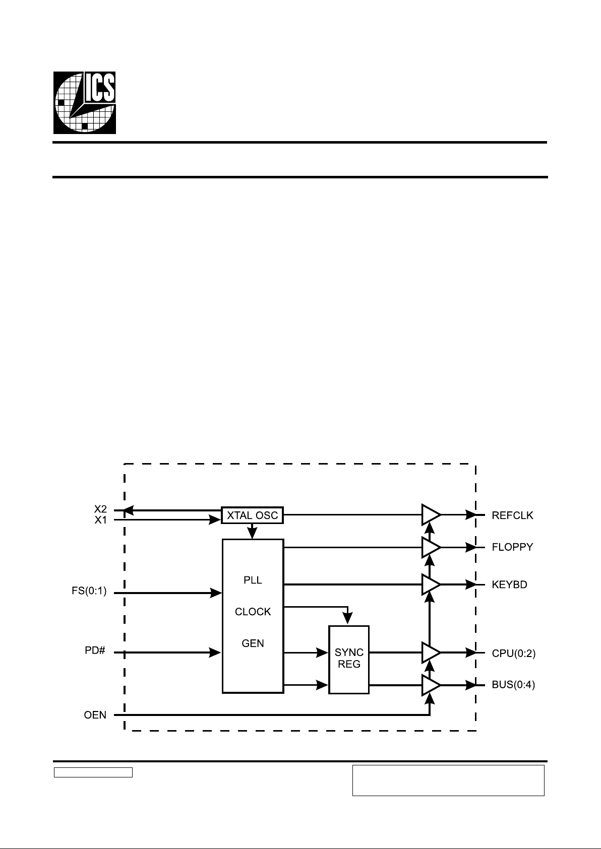
Block Diagram
9158-05 Rev B 05/08/97
Applications
The ICS9158-05 is a low cost frequency generator designed
specifically to clock Pentium systems using the Triton chip
set. Three copies of the CPU clock are available at 50, 60, or
66.7 MHz. Five copies of the synchronous BUS clock run at
half the CPU frequency. A 14.318 MHz REFCLK, 12 MHz,
KEYBD, and 24 MHz FLOPPY clock are also provided.
Each high drive output is capable of driving a 30pF load with
better than 1V/ns typical slew and have a duty cycle of 50±5%.
The synchronous outputs are skew controlled to within ±250ps
and CPU clocks lead BUS clocks by 2-5ns.
Glitch-free start and stop of the CPU and BUS clocks is
provided as well as a power-down mode with all clocks forced
low and the internal oscillators and PLLs powered-down.
Power-up time is less than 10ns. All frequency transitions are
gradual and meet the Intel cycle-to-cycle timing specification
for 486 and Pentium microprocessors.
• 3 CPU and 5 synchronous BUS clocks
• 50/60/66 MHz and glitch-free stop clock selections
• ±250ps skew between all synchronous outputs
• Outputs drive up to 30pF load with 1V/ns slew
• 2-5ns early CPU clocks support Triton chip set
• Compatible with 486 and Pentium CPUs
• Consumes less than 10µA in power-down mode
• On-chip loop filter components
• 3.0V - 5.5V supply range
• 24-pin SOIC package
• Ideal for RISC or CISC systems such as 486, Pentium,
PowerPC,™ etc. requiring multiple CPU and
synchronous BUS clocks.
Buffered Clock Generator for Pentium™ /Triton™ Systems
Advanced Information
Pentium and Triton are trademarks of Intel Corporation.
PowerPC is a trademark of Motorola Corporation
ADVANCE INFORMATION documents contain information on
new products in the sampling or preproduction phase of development. Characteristic data and other specifications are subject to
change without notice.
Page 2
2
ICS9158-05
Advanced Information
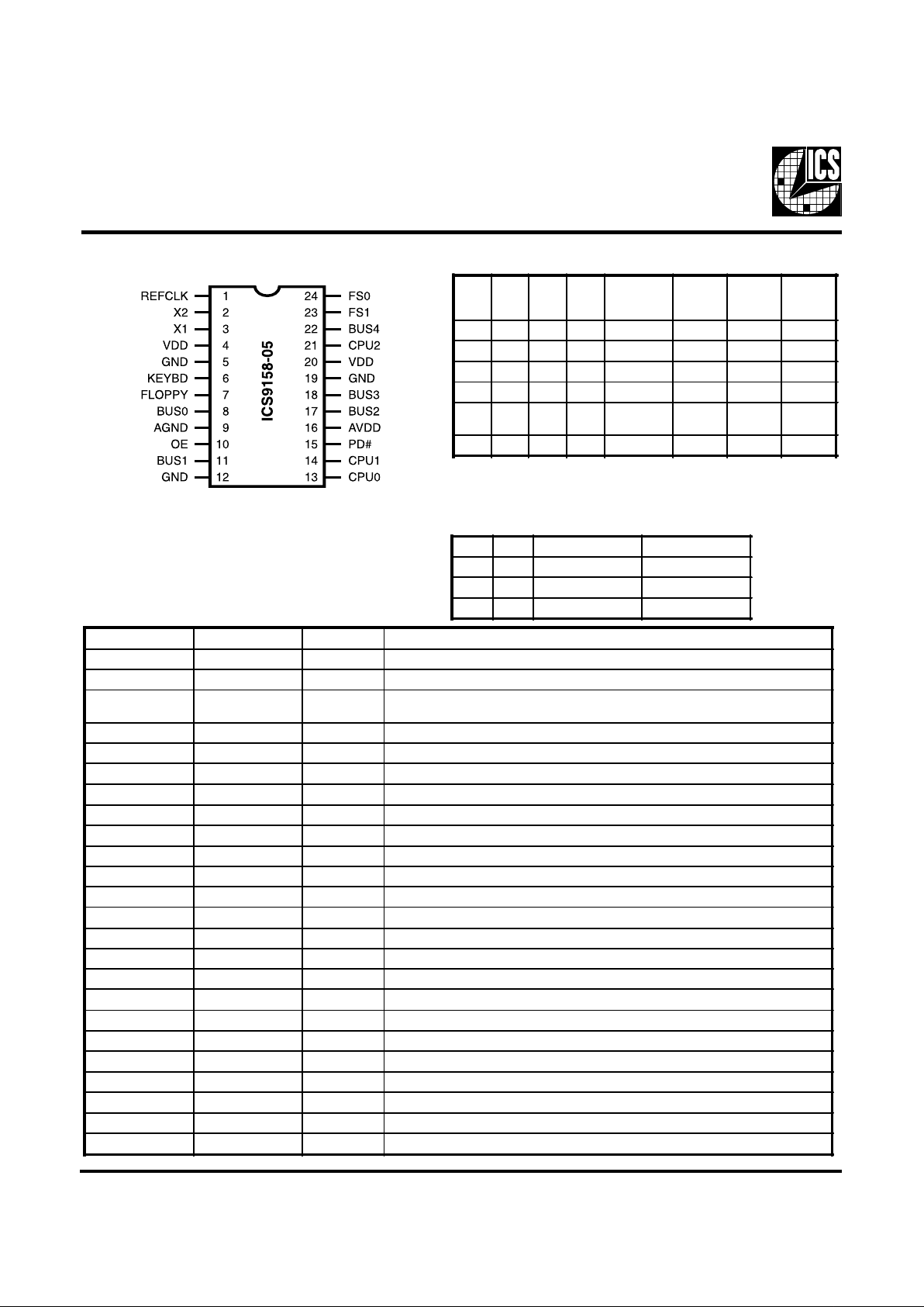
Pin Configuration
Pin Descriptions for ICS9158-05
24-Pin SOIC
* Input pin has internal pull-up to VDD.
Functionality
VDD = +5V±10%, TA=0°C to 70°C unless otherwise stated
PD# forces all outputs low and powers-down the oscillator and PLL
circuitry , minimizing power consumption. In order to ensure glitch-free start
and stop of the CPU and BUS clocks, PD# should be asserted after the
CPU and BUS clocks have stopped, and be deasserted 10ms (maximum
PLL lock time) prior to starting the clocks.
OE PD# FLOPPY (MHz) KEYBD (MHz)
1 1 24 12
1 0 Low Low
0 X Tristate Tristate
PIN NUMBER PIN NAME TYPE DESCRIPTION
1 REFCLK OUT 14.318 clock output.
2 X2 OUT Crystal connection, which includes output crystal load capacitance.
3X1 IN
Crystal connection, which includes crystal load capacitance and feedback bias
for a nominal 14.31818 MHz parallel-resonance 12pF crystal.
4 VDD PWR Digital POWER SUPPLY.
5 GND PWR Digital GROUND.
6 KEYBD OUT 12 MHz keyboard clock output.
7 FLOPPY OUT 24 MHz floppy disk clock output.
8 BUS0 OUT BUS clock output.
9 AGND PWR ANALOG GROUND.
10 OE IN OUTPUT ENABLE. Tristates all outputs when low.*
11 BUS1 OUT BUS clock output.
12 GND PWR Digital GROUND.
13 CPU0 OUT CPU clock output.
14 CPU1 OUT CPU clock output.
15 PD# IN Power-down input shuts off both PLL stages when low.*
16 AVDD PWR ANALOG power supply.
17 BUS2 OUT CPU clock output.
18 BUS3 OUT BUS clock output.
19 GND PWR Digital GROUND.
20 VDD PWR Digital POWER SUPPLY.
21 CPU2 OUT CPU clock output.
22 BUS4 OUT BUS clock output.
23 FS1 IN Clock frequency select #1.*
24 FS0 IN Clock frequency select #0.*
OE PD# FS1 FS0
CPU
Ratio
X1,X2,
REF
(MHz)
CPU
(0:2)
(MHz)
BUS
(0:4)
(MHz)
1 1 0 0 14/4xX1 14.318 50 25
1 1 0 1 14/3xX1 14.318 66.7 33.3
1 1 1 0 42/10xX1 14.318 60 30
1 1 1 1 (STOP) 14.318 Low Low
10XX
(PWR
DOWN)
Low *Low *Low
0 X X X - Tristate Tristate Tristate
Page 3
3
ICS9158-05
Advanced Information
Electrical Characteristics at 5V
Absolute Maximum Ratings
AVDD, VDD referenced to GND . . . . . . . . . . . . . . . . 7V
Operating temperature under bias. . . . . . . . . . . . . . . . 0°C to +70°C
Storage temperature . . . . . . . . . . . . . . . . . . . . . . . . . . -40°C to +150°C
Voltage on I/O pins referenced to GND. . . . . . . . . . . GND -0.5V to VDD +0.5V
Power dissipation . . . . . . . . . . . . . . . . . . . . . . . . . . . . 0.5 Watts
Stresses above those listed under Absolute Maximum Ratings may cause permanent damage to the device. This is a stress rating
only and functional operation of the device at these or any other conditions above those indicated in the operational sections
of the specifications is not implied. Exposure to absolute maximum rating conditions for extended periods may affect product
reliability.
DC Characteristics
PARAMETER SYMBOL TEST CONDITIONS MIN TYP MAX UNITS
Input Low Voltage V
IL
0.8 V
Input High Voltage V
IH
2.0 V
Input Low Current I
IL
VIN=0V (Pull-up) -20 µA
Input High Current I
IH
VIN=V
DD
-5 5 µA
Output Low Voltage V
OL
IOL=20.0mA 0.25 0.4 V
Output High Voltage
1
V
OH
IOH=-30mA 2.4 3.5 V
Output Low Current
1
I
OL
VOL=0.8V 45 6 5 mA
Output High Current
1
I
OH
VOH=2.0V -55 -35 mA
Supply Current I
DD
No load, 66 MHz 67 100 mA
Output Frequency Change over
Supply and Temperature
1
F
D
With respect to typical
frequency
0.002 0.01 %
Short circuit current
1
I
SC
Each output clock 25 56 mA
Pull-up resistor value
1
R
PU
Input pin 680 kΩ
Input Capacitance
1
C
i
Except X1, X2 8 pf
Load Capacitance
1
C
L
Pins X1, X2 20 pf
VDD = +5V±10%, TA=0°C to 70°C unless otherwise stated
Note 1: Parameter is guaranteed by design and characterization. Not 100% tested in production.
Page 4

4
ICS9158-05
Advanced Information
Electrical Characteristics (
continued
)
Note 1: Parameter is guaranteed by design and characterization. Not 100% tested in production.
AC Characteristics
PARAMETER SYMBOL TEST CONDI TIONS MIN TYP MAX UNITS
Output Rise time, 0.8 to 2.0V
(Note 1)
t
r
30pf load - 1 1.5 ns
Rise time, 20% to 80% V
DD
(Note 1)
t
r
30pf load - 2.5 3 ns
Output Fall time, 2.0 t o 0.8V
1
t
f
30pf load - 0.5 1.5 ns
Fall time, 80% to 20% V
DD
1
t
f
30pf load - 1.5 2 ns
Duty cycle
1
d
t
30pf load 45/55 48/52 55/45 %
Jitter, one sigma
1
t
j1s
As compared with clock
period
0.5 2.0 %
Jitter, absolute t
jab
-5 2 5 %
Jitter, absolute t
jab
25-66MHz clocks -250 250 ps
Input Frequency f
i
14.318 MHz
Clock skew between CPU and
2XCPU outputs
T
sk
100 250 ps
Frequency Transition Time
1
t
ft
From 4 to 50 MHz 13 20 ms
VDD = +5V±10%, TA=0°C to 70°C unless otherwise stated
Page 5

5
ICS9158-05
Advanced Information
VDD = +3.3V±10%, TA=0°C to 70°C unless otherwise stated
Electrical Characteristics at 3.3V
Note 1: Parameter is guaranteed by design and characterization. Not 100% tested in production.
DC Characteristics
PARAMETER SYMBOL TEST CONDITIONS MIN TYP MAX UNITS
Input Low Voltage V
IL
0.8 V
Input High Voltage V
IH
2.0 V
Input Low Current I
IL
VIN=0V(Pull-up) -10 µA
Input High Current I
IH
VIN=V
DD
-5 µA
Output Low Voltage V
OL
IOL=10mA 0.1V
DD
V
Output High Voltage
1
V
OH
IOH=-5mA 0.85V
DD
V
Output Low Current
1
I
OL
VOL=0.2V
DD
20 30 mA
Output High Current
1
I
OH
VOH=0.7V
DD
-15 -10 mA
Supply Current I
DD
No load, 66 MHz 43 65 mA
Output Frequency Change over
Supply and Temperature
1
F
D
With respect to typical
frequency
0.002 0.01 %
Short Circuit Current
1
I
SC
Each output clock 25 56 mA
Pull-up Resistor Value
1
R
PU
Input pin 900 kΩ
Input Capacitance
1
C
i
Except X1, X2 8 pF
Load Capacitance
1
C
L
Pins X1, X2 20 pF
AC Characteristics
PARAMETER
SYMBOL TEST CONDITIONS MIN TYP MAX UNITS
Output Rise time, 0.8 to 2.0V
1
t
r
30pF load - 1 3.0 ns
Rise time, 20% to 80% V
DD
1
t
r
30pF load - 2. 5 4.0 ns
Output Fall time, 2.0 to 0.8V
1
t
f
30pF load - 0. 5 2.5 ns
Fall time, 80% to 20% V
DD
1
t
f
30pF load - 1. 5 4.0 ns
Duty cycle
1
d
t
30pF load 40/50 44/46 50/40 %
Jitter, one sigma
1
t
j1s
As compared with clock
period
0.5 2.0 %
Jitter, absolute
1
t
jab
25%
Jitter, absolute
1
t
jab
25-66 MHz clocks 300 ps
Input Frequency f
i
14.318 MHz
Clock skew window between
CPU and 2XCPU outputs
1
T
sk
100 250 ps
Frequency Transition time
1
t
ft
From 4 to 50 MHz 13 20 ms
Page 6

6
ICS9158-05
Advanced Information
Frequency Transitions
A key feature of the ICS9158-05 is its ability to provide
smooth, glitch-free frequency transitions on the CPU and
BUS clocks when the frequency select pins are changed. The
frequency transition rate does not violate the Intel 486 or
Pentium specification of less than 0.1% frequency change
per clock period.
ICS9158-05 CPU Clock Decoding T able
(using 14.318 MHz input. All frequencies in MHz)
VDD=5V±10% or 3.3V±10%, TEMP=0-70°C
PD# forces all outputs low and powers-down the oscillator
and PLL circuitry, minimizing power consumption. In order
to ensure glitch-free start and stop of the CPU and BUS
clocks, PD# should be asserted after the CPU and BUS clocks
have stopped, and be deasserted 10ms (maximum PLL lock
time) prior to starting the clocks.
Using an Input Clock as a Reference
The ICS9158-05 is designed to accept a 14.318 MHz crystal
as the input reference. With some external changes, it is
possi-ble to use a crystal oscillator or other clock sources.
Please see application note AAN04 for details on driving the
ICS9158-05 with a clock.
OE PD# FS1 FS0
CPU
Ratio
X1,X2,
REF
(MHz)
CPU
(0:2)
(MHz)
BUS
(0:4)
(MHz)
110014/4xX1 14.318 50 25
110114/3xX1 14.318 66. 7 33. 3
111042/10xX1 14.318 60 30
1111(STOP) 14.318 Low Low
10XX
(PWR
DOWN)
Low *Low *Low
0 X X X - Tristate Tristate Tristate
OE PD# FLOPPY (MHz) KEYBD (MHz)
1 1 24 12
1 0 Low Low
0 X Tristate Tristate
Page 7

7
ICS9158-05
Advanced Information
Ordering Information
ICS9158-05M
Example:
ICS XXXX-PPP M
Package Type
M=SOIC
Pattern Number (2 or 3 digit number for parts with ROM code patterns)
Device Type (consists of 3 or 4 digit numbers)
Prefix
ICS, A V=Standard Device; GSP=Genlock Device
24 Lead SOIC
LEAD COUNT 24L
DIMENSION L 0.604
ADVANCE INFORMATION documents contain information on
new products in the sampling or preproduction phase of development. Characteristic data and other specifications are subject to
change without notice.
 Loading...