

Page 1
Integrated
Circuit
Systems, Inc.
General Description Features
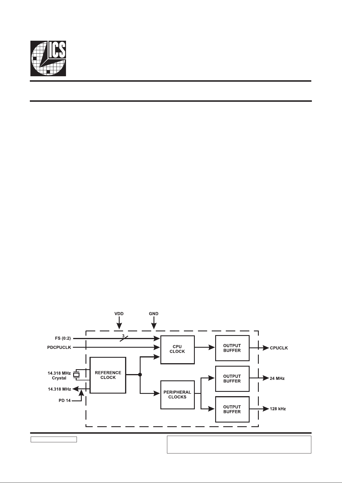
AV9154A-60
Block Diagram
9154-60 Rev B 05/30/97
Applications
OPTi Notebook Frequency Generator
The AV9154A-60 is a low cost frequency generator designed
for general purpose PC and disk drive applications. Its CPU
clocks provide all necessary frequencies for 286, 386 and
486 systems, including support for the latest speeds of
processors. The standard devices use a 14.318 MHz crystal to
generate the CPU and peripheral clocks for integrated desktop
and notebook motherboards.
The AV9154A-60 is specifically designed for use with OPTi
core logic chip sets.
The AV9154A-60 can operate at 5.0V±10% or 3.3V±10%,
but the CPU frequencies are limited (see the asterisks on the
selection tables on page three) during 3.3V operation. The
parts have two power-down pins. One shuts off the CPU clock
to a low state when the power-down pin is taken high, and the
other turns off the 14.318 MHz output in the same manner.
Computer Motherboards: The AV9154A-60 replaces crystals
and oscillators, saving board space, component cost, part
count and inventory costs. It produces switchable CPU clock
and up to four fixed clocks to drive floppy disk,
communications, super I/O, bus and/or keyboard devices. The
small package and 3.3V operation is perfect for handheld
computers.
• Compatible with 286, 386, and 486 CPUs
• Up to 66.6 MHz (-60) CPU clocks
• All loop filter components internal
• 3.3V and 5V operation
• 16-pin 150-mil SOIC
• Power-down control of CPU clock
ICS reserves the right to make changes in the device data identified in this
publication without further notice. ICS advises its customers to obtain the latest
version of all device data to verify that any information being relied upon by the
customer is current and accurate.
Page 2
2
AV9154A-60
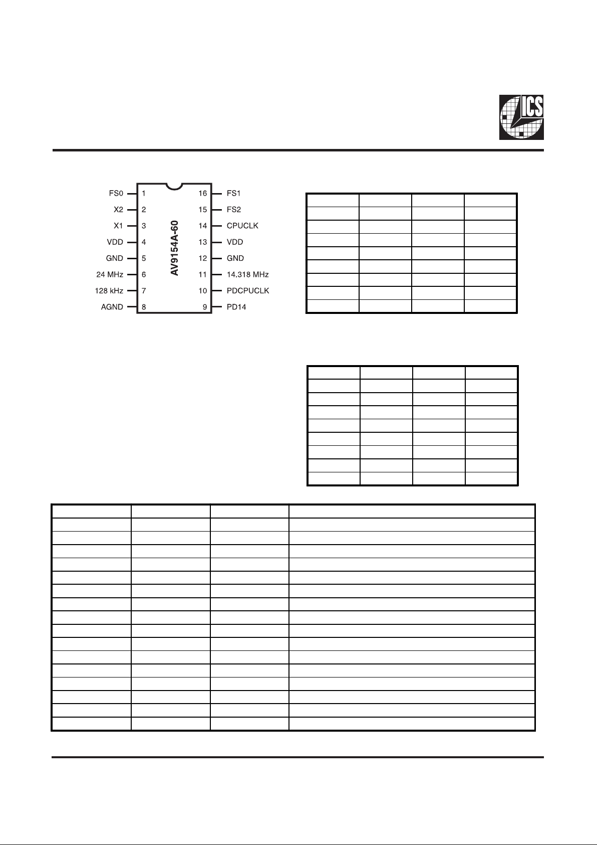
Pin Configuration
Pin Descriptions
16-Pin SOIC
Note:
No internal pull-ups on any Inputs.
* Frequencies shown are assuming a 14.318 MHz input.
Functionality
(in MHz, assuming 14.318 MHz input)
Actual Output Frequencies
(in MHz, assuming 14.318 MHz input)
PIN NUMBER PIN NAME TYPE DESCRIPTION
1 FS0 I Frequency Select 0 for C PUCLK.
2 X2 O Crystal out. Connect a 14.318 MHz crystal to this pin.
3 X1 I Crystal in. Connect a 14.318 MHz crystal to this pin.
4 VDD P Digital Power (+3.3V or +5V).
5 GND P Digital Ground.
6 24 Mhz O 24 MHz clock output.*
7 128 kHz O 128 kHz clock output.*
8 AGND P Analog Ground.
9 PD14 I Power-down 14.318 MHz output (active high).
10 PDCPUCLK I Power-down CPU clock (active high).
11 14.318 Mhz O 14.318 MHz reference clock output .*
12 GND P Digital Ground.
13 VDD P Digital Power (+3.3V or +5V).
14 CPUCLK O CPU Clock output determined by status of FS0 - FS2.
15 FS2 I Frequency Select 2 for CPUCLK.
16 FS1 I Frequency Select 1 for CPUCLK.
FS2 FS1 FS0 CPUCLK
0008
00116
01020
01125
10033.33
10140
11050
11166.66
FS2 FS1 FS0 CPUCLK
0008.182
00116.11
01020.05
01125.06
10033.24
10140.09
11050.11
11166.48
Page 3
3
AV9154A-60
Electrical Characteristics at 5V
Absolute Maximum Ratings
VDD referenced to GND . . . . . . . . . . . . . . . . . . . . . . 7V
Operating temperature under bias. . . . . . . . . . . . . . . . 0°C to +70°C
Storage temperature . . . . . . . . . . . . . . . . . . . . . . . . . . -40°C to +150°C
Voltage on I/O pins referenced to GND. . . . . . . . . . . GND -0.5V to VDD +0.5V
Power dissipation . . . . . . . . . . . . . . . . . . . . . . . . . . . . 0.5 Watts
Stresses above those listed under Absolute Maximum Ratings may cause permanent damage to the device. This is a stress rating
only and functional operation of the device at these or any other conditions above those indicated in the operational sections
of the specifications is not implied. Exposure to absolute maximum rating conditions for extended periods may affect product
reliability.
VDD =+5V±10%, TA=0°C to 70°C unless otherwise stated
Note:
1. Parameter is guaranteed by design and characterization. Not 100% tested in production.
2. All clocks on AV9154A-60 running at highest possible frequencies.
DC Charac teristics
PARAMETER SYMBOL TEST CONDITIONS MIN TYP MAX UNITS
Input Low Vo ltage V
IL
VDD=5V - - 0.8 V
Input High Voltage V
IH
VDD=5V 2.0 - - V
Input Low Current I
IL
VIN=0V - - -5 µA
Input High Current I
IH
VIN=V
DD
--5µA
Output Low Voltage
1
V
OL
IOL=10mA - 0.15 0.4 V
Output High Voltage
1
V
OH
IOH=-30mA 2.4 3.7 - V
Output Low Current
1
I
OL
VOL=0.8V 15 32 - mA
Output High Current
1
I
OH
VOH=2.4V - -48 -30 mA
Supply Current I
DD
No load
2
-2550mA
Output Frequency Change over
Supply and Temperature
1
F
D
With respect to typical
frequency
- 0.002 0.01 %
Short circuit current
1
I
SC
Each output clock 25 40 - mA
Input Capacitance
1
C
i
Except X1, X2 - - 10 pF
Load Capacitance
1
C
L
Pins X1, X2 - 20 - pF
Supply Current, lowest I
DDSTBY
When powered-down - 20 - mA
Page 4

4
AV9154A-60
Electrical Characteristics at 5V
VDD =+5V±10%, TA=0°C to 70°C unless otherwise stated
Note:
1. Parameter is guaranteed by design and characterization. Not 100% tested in production.
AC Charac teristics
PARAMETER SYMBOL TEST CONDITIONS MIN TYP MAX UNITS
Input Clock Rise time
1
t
ICr
20 ns
Input Clock Fall time
1
t
ICf
20 ns
Output Rise tim e
1
t
r
15pF load, 0.8 to 2.0V - 1 2 ns
Rise time
1
t
r
15pF load, 20% to 80 % V
DD
-24ns
Output Fall time
1
t
f
15pF load, 2.0 to 0.8V - 1 2 ns
Fall time
1
t
f
15pF load, 80% to 20 % V
DD
-24ns
Duty cycle
1
d
t
15pF load 40 /60 48/52 60/40 %
Duty cycle, reference clock
1
d
t
15pF load 40 /60 43/57 60/40 %
Jitter, one sigma
1
T
jls
As compared with clock
period
±0.8 ±2.5 %
Jitter, absolute
1
T
jab
±2 ±5 %
Jitter, absolute
1
T
jab
16-80 MHz clock s 700 ps
Input Frequency
1
f
i
14.318 MHz
Frequency Transition time
1
t
ft
From 16 to 80 M Hz 15 20 ms
Power-up time
1
t
pu
From off to 50 MHz 15 ms
Page 5

5
AV9154A-60
Electrical Characteristics at 3.3V
Operating V
DD
=+3.0V to +3.7V, TA=0°C to 70°C unless otherwise stated
Note:
1. Parameter is guaranteed by design and characterization. Not 100% tested in production.
2. All clocks on AV9154A-60 running at highest possible frequencies.
DC Charac teristics
PARAMETER SYMBOL TEST CONDITIONS MIN TYP MAX UNITS
Input Low Voltage V
IL
--0.2VDDV
Input High Voltage V
IH
0.7V
DD
--V
Input Low Current I
IL
VIN=0V -5 - 5 µ A
Input High Current I
IH
VIN=V
DD
-5 - 5 µ A
Output Low Voltage
1
V
OL
IOL=6mA - 0.05V
DD
0.1V
DD
V
Output High Voltage
1
V
OH
IOH=-4mA 0.85V
DD
0.94V
DD
-V
Supply Current I
DD
Note 2, no load - 15 27 m A
Output Low Current
1
I
OL
VOL=0.2V
DD
12 22 - mA
Output High Current
1
I
OH
VOH=0.7V
DD
--11-6.5mA
Output Frequency Change over
Supply and Temperature
1
F
d
With respect to typical
frequency
- 0.002 0.01 %
Input Capacitance
1
C
i
Except X1, X2 - - 10 pF
Load Capacitance
1
C
L
Pins X1, X2 - 20 - pF
Supply Current, lowest I
DDL
When powered-down - 14 - mA
Short Circuit Current
1
I
SC
-30-mA
Page 6

6
AV9154A-60
Electrical Characteristics at 3.3V
Operating V
DD
=+3.0V to +3.7V, TA=0°C to 70°C unless otherwise stated
Note:
1. Parameter is guaranteed by design and characterization. Not 100% tested in production.
AC Charac teristics
PARAMETER SYMBOL TEST CONDITIONS MIN TYP MAX UNITS
Input Clock Rise time
1
t
ICr
- - 20 ns
Input Clock Fall time
1
t
ICf
- - 20 ns
Rise time
1
t
r
15pF load - - 4 ns
Fall time
1
t
f
15pF load - - 4 ns
Duty cycle, fixed clocks
1
d
t
15pF load 40/60 48/52 60/40 %
Duty cycle, reference clock
1
d
t
15pF load 40/60 43/57 60/40 %
Jitter, one sigma
1
, 20-66 MHz T
jls1
- 10 0 200 ps
Jitter, one sigma
1
,
below 20 MHz
T
jls2
-0.52%
Jitter, absolute
1
, 20-66 Mhz T
jabs1
-350 ±165 350 ps
Jitter, absolute
1
, below 20 Mhz T
jabs2
-5 ±3 ±5 %
Frequency Transition time
1
t
ft
from 8 to 33 Mhz - - 20 ms
Power-up time
1
t
pu
from off to 50 Mhz - 15 - ms
Output Frequency
1
f
o
233MHz
Input Frequency
1
f
i
- 14.318 - MHz
Page 7

7
AV9154A-60
Ordering Information
A V9154A-60CS16
Example:
ICS XXXX-PPP M X#W
16-Pin SOIC Pac kage
Lead Count & Package Width
Lead Count=1, 2 or 3 digits
W=.3” SOIC or .6” DIP; None=Standard Width
Package Type
S=SOIC
Pattern Number (2 or 3 digit number for parts with ROM code patterns)
Device Type (consists of 3 or 4 digit numbers)
Prefix
ICS, A V=Standard Device; GSP=Genlock Device
ICS reserves the right to make changes in the device data identified in this
publication without further notice. ICS advises its customers to obtain the latest
version of all device data to verify that any information being relied upon by the
customer is current and accurate.
 Loading...