

Page 1
Integrated
Circuit
Systems, Inc.
Preliminary Product Preview
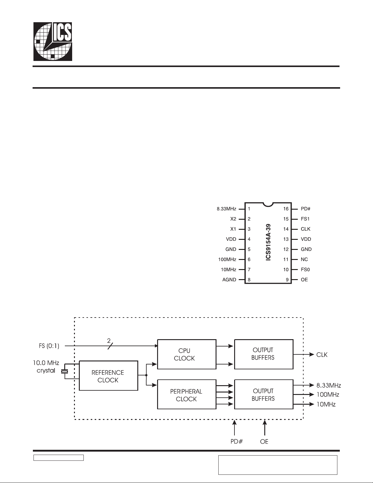
Low Cost 16-Pin Frequency Generator
AV9154A-39
General Description
The ICS9154A-39 is a 0.8mm technology low-cost frequency
generator designed for general purpose PC and disk drive
applications. However, because the ICS9154A-39 uses 0.8mm
technology and the latest phase-locked loop architecture, it
offers significant performance advantages that enable the
device to be used in high performance systems when clock
jitter is a key design issue.
The ICS9154A-39 guarantees a 45/55 duty cycle over all
frequencies. In addition, a worst case jitter of ±250ps is
achieved.
The CPU clock offers the unique feature of smooth, glitchfree transitions from one frequency to the next, making this
the ideal device to use whenever slowing the cpu speed. The
ICS9154A-39 makes a gradual transition between
frequencies.
Features
All loop filter components internal
5V operation
16-pin 150-mil SOIC
Power-down control of CPU clock and Fixed Clock
when PD# goes low
Output enable control of all output pins
Pin Configuration
Block Diagram
9154-39 Rev B 09/18/97
16-Pin SOIC
PRODUCT PREVIEW documents contain information on new
products in the sampling or preproduction phase of development.
Characteristic data and other specifications are subject to change
without notice.
Page 2
AV9154A-39
Preliminary Product Preview
Pin Descriptions
PIN
NUMBER
1 8.33 MHz OUT 8.33 MHz output clock.*
2 X2 OUT Crystal Out.
3 X1 IN Crystal In, nominally 10.0 MHz.
4 VDD PWR Digital power (+5V).
5 GND PWR Digital ground.
6 100 MHz OUT 100 MHz clock output.*
7 10 MHz OUT 10 MHz keyboard clock output.*
8 AGND PWR Analog ground.
9 OE IN Tristates outputs when low.
10 FS0 IN Frequency select 0 for CPU clock.
11 NC - No connect (Do not connect to this pin.).
12 GND PWR Digital ground.
13 VDD PWR Digital power (+5V).
14 CPUCLK OUT CPU clock output.
15 FS1 IN Frequency select 1 for CPU clock.
16 PD# IN
PIN NAME TYPE DESCRIPTION
Power-down, shuts off internal clocks and forces outputs to
low logic level when input pulled logic low.
Note: The following input pins are pulled-up to VDD internal: 9, 10, 15 and 16.
Functionality
FS1 FS0 CLK(MHz)
0 0 40.0
0 1 30.0
1 0 37.0
1 1 25.0
These frequencies assume an input frequency of 10.0 Mhz.
2
Page 3

AV9154A-39
Preliminary Product Preview
Absolute Maximum Ratings
VDD referenced to GND . . . . . . . . . . . . . . . . . . . . . . 7V
Voltage on I/O pins referenced to GND. . . . . . . . . . . GND -0.5V to VDD +0.5V
Operating temperature under bias. . . . . . . . . . . . . . . . 0°C to +70°C
Power dissipation . . . . . . . . . . . . . . . . . . . . . . . . . . . . 0.5 Watts
Storage temperature . . . . . . . . . . . . . . . . . . . . . . . . . . -40°C to +150°C
Stresses above those listed under Absolute Maximum Ratings may cause permanent damage to the device. This is a stress rating
only and functional operation of the device at these or any other conditions above those indicated in the operational sections
of the specifications is not implied. Exposure to absolute maximum rating conditions for extended periods may affect product
reliability.
Electrical Characteristics at 5V
VDD = +5V±10%, TA=0°C to 70°C
DC Characteristics
PARAM ETER SYMBOL TEST CONDITIONS MIN TYP MAX UNITS
Input Low Voltage V
Input High Voltage V
Input Low Current I
Input High Current I
Output Low Voltage V
Output High Voltage
Output Low Current
Output High Current
1
1
1
Supply Current I
Output Frequency Change over
Supply and Temperature
Input Capacitance
Load Capacitance
1
1
1
IL 0.8 V
IH 2.0 V
IL VIN=0V -35 -16.0 µA
IH VIN=VDD -5 5 µ A
OL IOL=10mA 0.15 0.4 V
VOH IOH=-30mA 2.4 3.7 V
IOL VOL=0.8 15 32 mA
IOH VOH=2.0V -48 -30 mA
DD Unloaded, 40 MHz 25 50 mA
FD
With respect to typical
frequency
0.002 0.01 %
CI Except X1, X2 10 pF
CL
Pins X1, X2 20 pF
Notes:
1. Parameter is guaranteed by design and characterization, not subject to production testing.
3
Page 4

AV9154A-39
Preliminary Product Preview
Electrical Characteristics at 5V
VDD = +5V±10%, TA=0°C to 70°C
PARAMETER SYMBOL TEST CONDITIONS MIN TYP MAX UNITS
Input Clock Rise Time
Input Clock Fall Time
Output Rise time
Rise time
1
Output Fall time
Fall time
Duty cycle
1
1
Duty cycle, reference clocks
Jitter, one sigma, 32 MHz-100
MHz clocks
Jitter, one sigma, 16 MHz-30
MHz clocks
Jitter, one sigma, clocks below
16 MHz
Jitter, absolute, 32 MHz-100
MHz clocks
Jitter, absolute, 16-30 MHz
clock
Jitter, absolute, clocks below 16
MHz
Input Frequency
Power-up Time
1
1
1
1
1
1
1
Frequency Transition Time
1
1
1
tICr 20 ns
tICf 20 ns
tr 15pF load, 0.8 to 2.0V - 0.8 2 ns
tr
1
tf 15pF load, 2.0 to 0.8V - 0.7 2 ns
tf
1
dt 1 5pF load @ 1.4V 45 55 %
dt 1 5pF load @ 1.4V 40 60 %
tjls 80 120 ps
tjls 100 150 ps
tjls 400 500 ps
tjab -250 250 ps
tjab -700 700 ps
tjab -2 2 ns
1
1
fin 10.0 MHz
tPO to 100 MHz 10 20 ms
tft from 25.0 to 4 0.0 MHz 8 ms
AC Characteristics
15pF load,
20% to 80% VDD
15pF load,
80% to 20% VDD
-1.43ns
-0.82ns
Notes: 1. Parameter is guaranteed by design and characterization, not subject to production testing.
ICS9154A-39
Figure 1: Typical Crystal Circuitry
Note: Crystal load capacitors are internal to the ICS9154A-39 device and no external components are required.
4
Page 5

Preliminary Product Preview
16-Pin SOIC Package
AV9154A-39
Ordering Information
AV9154A-39CS16
Example:
XXX XXXX-PPP M X#W
Lead Count & Package Width
Lead Count=1, 2 or 3 digits
W=.3 SOIC or .6 DIP; None=Standard Width
Package Type
S=SOIC
Pattern Number (2 or 3 digit number for parts with ROM code patterns)
Device Type (consists of 3 or 4 digit numbers)
Prefix
ICS, AV=Standard Device; GSP=Genlock Device
PRODUCT PREVIEW documents contain information on new
5
products in the sampling or preproduction phase of development.
Characteristic data and other specifications are subject to change
without notice.
 Loading...