

Page 1
Integrated
Circuit
Systems, Inc.
General Description Features
ICS9148-58
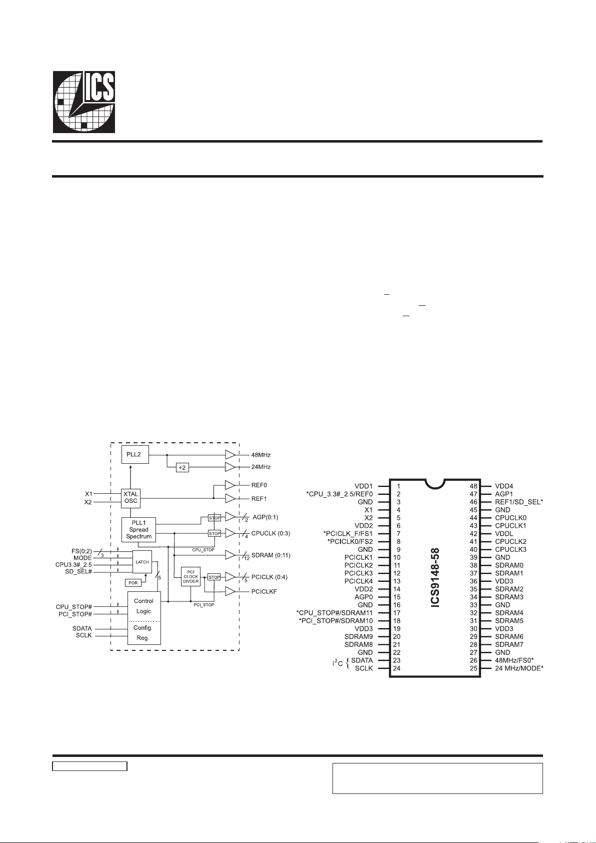
Block Diagram
Pentium is a trademark of Intel Corporation
I2C is a trademark of Philips Corporation
Frequency Generator & Integrated Buffers for PENTIUM/Pro
TM
9148-58 Rev C 12/07/98
Pin Configuration
Generates the following system clocks:
- 4 CPU(2.5V/3.3V) upto 100MHz.
- 6 PCI(3.3V) @ 33.3MHz
- 2AGP(3.3V) @ 2 x PCI
- 12 SDRAMs(3.3V) @ either CPU or AGP
- 2 REF (3.3V) @ 14.318MHz
Skew characteristics:
- CPU CPU<250ps
- SDRAM SDRAM < 250ps
- CPU SDRAM < 250ps
- CPU(early) PCI : 1-4ns
Spread Spectrum 0 to -5% down spread.
Serial I2C interface for Power Management, Frequency
Select, Spread Spectrum.
Efficient Power management scheme through PCI and CPU
STOP CLOCKS.
Uses external 14.318MHz crystal
48 pin 300mil SSOP.
48-Pin SSOP
Power Groups
VDD1 = REF (0:1), X1, X2
VDD2 = PCICLK_F, PCICLK(0:5)
VDD3 = SDRAM (0:11), supply for PLL core,
24 MHz, 48MHz
VDD4 = AGP (0:1)
VDDL = CPUCLK (0:3)
* Internal Pull-up Resistor of
240K to 3.3V on indicated inputs
The ICS9148-58 is the single chip clock solution for Desktop/
Notebook designs using the VIA MVP3 style chipset. It
provides all necessary clock signals for such a system.
Spread spectrum may be enabled through I2C programming.
Spread spectrum typically reduces system EMI by 8dB to
10dB. This simplifies EMI qualification without resorting to
board design iterations or costly shielding. The ICS9148-58
employs a proprietary closed loop design, which tightly
controls the percentage of spreading over process and
temperature variations.
Serial programming I2C interface allows changing functions,
stop clock programming and frequency selection. The SD_SEL
latched input allows the SDRAM frequency to follow the
CPUCLK frequency(SD_SEL=1) or the AGP clock
frequency(SD_SEL=0)
ICS reserves the right to make changes in the device data identified in
this publication without further notice. ICS advises its customers to
obtain the latest version of all device data to verify that any
information being relied upon by the customer is current and accurate.
Page 2
2
ICS9148-58
Pin Descriptions
Notes:
1: Internal Pull-up Resistor of 240K to 3.3V on indicated inputs
2: Bidirectional input/output pins, input logic levels are latched at internal power-on-reset. Use 10Kohm resistor to
program logic Hi to VDD or GND for logic low.
PIN NUMBER PIN NAME TYPE DESCRIPTION
1 VDD1 PWR Ref (0:2), XTAL power supply, nominal 3.3V
2
REF0 OUT 14.318 MHz reference clock.
CPU3.3#_2.5
1,2
IN
Indicates whether VDDL2 is 3.3V or 2.5V. High=2.5V CPU, LOW=3.3V
CPU
1
. Latched input
2
3,9,16,22,27,
33,39,45
GND PWR Ground
4X1 IN
Crystal input, has internal load cap (33pF) and feedback
resistor from X2
5X2 OUT
Crystal output, nominally 14.318MHz. Has internal load
cap (33pF)
6,14 VDD2 PW R Supply for PCICLK_F and PCICLK (0:5), nominal 3.3V
7
PCICLK_F OUT
Free running PC I clock output. Synchrounous wi th CPUCLKs with 1-4n s
skew (CPU early) This is not affected by PCI_STOP#
FS1
1, 2
IN
Frequency sel ect pin. Latche d Input. Along with other FS pi ns determins the
CPU, SDRAM, PCI & AGP frequencies.
8
PCICLK0 OU T PCI clock output. S ynchrounous CPUCLKs wi th 1-4ns skew (CPU ea rly)
FS2
1, 2
IN
Frequency sel ect pin. Latche d Input Along wi th other FS pins determins the
CPU, SDRAM, PCI & AGP frequencies.
10, 11, 12, 13 PCICLK(1:4) OU T PCI clock outputs. S ynchrounous CPUCLK s with 1-4ns skew (CPU ea rly)
15, 47 AGP (0:1) OU T Advanced Graphic Port o utputs, powered by VDD 4.
17
CPU_STOP#
1
IN
This asyncherono us input halt s CPUCLK (0:3) an d AGP (0:1) clocks at
logic 0 level, when input low (in Mobile Mode, MODE=0)
SDRAM 11 OU T
SDRAM clock out put. Frequenc y is selected by the SD_SEL latched inpu t.
SD_SEL = 1 at power on causes SDRAM frequen cy = CPU frenquenci es
SD_SEL = 0 at power on causes SDRAM frequen cies = AGP frequencies
18
PCI_STOP#
1
IN
This asyncher onous input ha lts PCICLK(0 :5) clocks at lo gic 0 level, when
input low (In mobile mode, MODE=0)
SDRAM 10 OU T
SDRAM clock out put. Frequenc y is selected by the SD_SEL latched inpu t.
SD_SEL = 1 at power on causes SDRAM frequen cy = CPU frenquenci es
SD_SEL = 0 at power on causes SDRAM frequen cies = AGP frequencies
20, 21,28, 29, 31,
32, 34, 35,37,38
SDRAM (0:9) O UT
SDRAM clock outputs. Frequency is selected by the SD_SEL latched input.
SD_SEL = 1 at power on causes SDRAM frequen cy = CPU frenquenci es
SD_SEL = 0 at power on causes SDRAM frequen cies = AGP frequencies
19,30,36 VDD3 PW R
Supply for SDRAM (0:11), CPU Core and 24 , 48MHz clocks,
nominal 3.3V.
23 SDATA I N Data input for I
2
C serial input.
24 SCLK IN Clock input of I
2
C input
25
24MHz OU T 24MHz output cloc k, for Super I/O timi ng.
MODE
1, 2
IN
Pin 17, pin 18 f unction sele ct pin, 1=Deskto p Mode, 0=Mo bile Mode.
Latched Inpu t.
26
48MHz OU T 48MHz output cloc k, for USB timin g.
FS0
1, 2
IN
Frequency sel ect pin. Latche d Input Along wi th other FS pins determins the
CPU, SDRAM, PCI & AGP frequencies.
40, 41, 43, 44 CPUCLK(0:3) O UT CPU clock outputs, powered by VDDL2. Low if CPU_STOP#=Low
42 VDDL PW R Supply for CPU (0:3), either 2. 5V or 3.3V nominal
46
REF1 O U T 14.318MHz reference clock.
SD_SEL IN
Latched input at Power On selec ts either CPU (SDSEL=1) or AGP
(SD_SEL=0) frequencies for the SDRAM clock outputs.
48 VDD 4 PW R Supply for AGP (0:1)
Page 3
3
ICS9148-58
Functionality
VDD1, 2, 3, 4 = 3.3V±5%, V
DDL
= 2.5V ±5% or 3.3 ±5%, TA= 0 to 70°C
Crystal (X1, X2) = 14.31818MHz
CPU3.3#_2.5
Input level
(Latch ed Data )
Buffer Selected for
operation at:
12.5V VDD
03.3V VDD
CPU 3.3#_2.5V Buffer selector for CPUCLK drivers.
Power Management Functionality
Mode Pin - Power Management Input Control
MODE, Pin 25
(Latched Input)
Pin 17 Pin 18
0
CPU_STOP#
(INPUT)
PCI_STOP#
(INPUT)
1
SDRAM 11
(OUTPUT)
SDRAM 10
(OUTPUT)
CPU_STOP# PCI_STOP#
AGP,
CPUCLK
Outputs
PCICLK
(0:5)
PCICLK_F,
REF,
24/48MHz
and SDRAM
Crystal
OSC
VCO
0 1 Stopped Low Running Running Running Running
1 1 Running Run ning Runnin g Running Running
1 0 Running Stopped Low Running Running Running
FS2 FS1 FS0
CPU
(M Hz)
SDRAM (MHz)
PC I (M Hz) AGP (MH z)
SD _SEL= 1 S D_S EL=0
1 1 1 100.2 100.2 66.6 33.3 66.6
1 1 0 95.25 95.25 63.5 31.75 63.5
1 0 1 83.3 83.3 66.6 33.3 66.6
1 0 0 133.3 133.3 88.7 44.3 88.7
011 75 75 75 37.5 75
0 1 0 124 124 82.7 41.3 82.7
0 0 1 66.8 66.8 66.8 33.4 66.8
0 0 0 112 112 74.7 37.3 74.7
Page 4
4
ICS9148-58
Byte0: Functionality and Frequency Select Register
(default = 0)
Serial Configuration Command Bitmap
Bit Description PWD
Bit 7 Reserved 0
Bit
6:4
Bit6 Bit5
Bit4
111
110
101
100
011
010
001
000
CPU Clock
100.2
95.25
83.3
133.3
75
124
66.8
112
PCI
33.3
31.75
33.3
44.3
37.5
41.3
33.4
37.3
AGP
66.6
63.5
66.6
88.7
75
82.7
66.8
74.7
Note
1
Bit 3
0 - Frequency is sel ect ed by har dware sel ect ,
Latched I nputs
1 - Frequency is sel ect ed by Bit 6:4 ( above)
0
Bit 2
0 - Spread Spectr um cent er sprea d type . ±.25%
1 - Spread Spectrum down spread type. 0 to - .5%
0
Bit 1
0 - Normal
1 - Spread Spectrum Enabled
0
Bit 0
0 - Running
1- Tristate all outputs
0
General I2C serial interface information
The information in this section assumes familiarity with I2C programming. For more information, contact ICS for an I2C
programming application note.
How to Write:
Send the address D2
(H)
.
Send two additional dummy bytes, a command code
and byte count.
Send the desired number of data bytes.
See the diagram below:
Note that the acknowledge bit is sent by the clock chip, and pulls the data line low. There is no minimum of data bytes that must
be sent.
How to Read:
Send the address D3
(H)
.
Send the byte count in binary coded decimal
Read back the desired number of data bytes
See the diagram below:
The following specifications should be observed:
1. Operating voltage for I2C pins is 3.3V
2. Maximum data transfer rate (SCLK) is 100K bits/sec.
Clock Generator
Address (7 bits)
ACK
+ 8 bits
dummy
command code
ACK
+ 8 bits
dummy Byte
count
ACK
Data Byte
1
ACK
Data Byte
N
ACK
A(6:0) & R/W#
D2
(H)
Clock Generator
Address (7 bits)
ACK
Byte
Count
ACK
Data Byte
1
ACK
Data Byte
N
A(6:0) & R/W#
D3
(H)
I2C is a trademark of Philips Corporation
Note 1. Default at Power-up will be for latched logic inputs
to define frequency. Bits 4, 5, 6 are default to 000,
and if bit 3 is written to a 1 to use Bits 6:4, then
these should be defined to desired frequency at same
write cycle.
Note: PWD = Power-Up Default
Page 5
5
ICS9148-58
Byte 1: CPU, Active/Inactive Register
(1 = enable, 0 = disable)
Byte 2: PCI Active/Inactive Register
(1 = enable, 0 = disable)
Byte 3: SDRAM Active/Inactive Register
(1 = enable, 0 = disable)
Notes:
1. Inactive means outputs are held LOW and are disabled
from switching.
Notes:
1. Inactive means outputs are held LOW and are disabled
from switching.
Notes:
1. Inactive means outputs are held LOW and are disabled
from switching.
Bit Pin # PWD Description
Bit 7 - 1 (Reserved)
Bit 6 - 1 (Reserved)
Bit 5 - 1 (Reserved)
Bit 4 - 1 (Reserved)
Bit 3 40 1 CPUCLK3 (Act/Inact)
Bit 2 41 1 CPUCLK2 (Act/Inact)
Bit 1 43 1 CPUCLK1 (Act/Inact)
Bit 0 44 1 CPUCLK0 (Act/Inact)
Bit Pin # PWD Description
Bit 7 - 1 (Reserved)
Bit 6 7 1 PCICLK_F (Act/Inact)
Bit 5 15 1 AGP0 (Act/Inact)
Bit 4 14 1 PCICLK4 (Act/Inact)
Bit 3 12 1 PCICLK3 (Act/Inact)
Bit 2 11 1 PCICLK2 (Act/Inact)
Bit 1 10 1 PCICLK1 (Act/Inact)
Bit 0 8 1 PCICLK0(Act/Inact)
Bit Pin # PWD Description
Bit 7 28 1 SDRAM7 (Act/Inact)
Bit 6 29 1 SDRAM6 (Act/Inact)
Bit 5 31 1 SDRAM5 (Act/Inact)
Bit 4 32 1 SDRAM4 (Act/Inact)
Bit 3 34 1 SDRAM3 (Act/Inact)
Bit 2 35 1 SDRAM2 (Act/Inact)
Bit 1 37 1 SDRAM1 (Act/Inact)
Bit 0 38 1 SDRAM0 (Act/Inact)
Byte 4: SDRAM Active/Inactive Register
(1 = enable, 0 = disable)
Byte 5: Peripheral Active/Inactive Register
(1 = enable, 0 = disable)
Notes:
1. Inactive means outputs are held LOW and are disabled
from switching.
Notes:
1. Inactive means outputs are held LOW and are disabled
from switching.
Bit Pin # PWD Description
Bit 7 - 1 (Reserved)
Bit 6 - 1 (Reserved)
Bit 5 - 1 (Reserved)
Bit 4 - 1 (Reserved)
Bit 3 17 1
SDRAM11 (Act/Inact)
(Desktop Mode Onl y)
Bit 2 18 1
SDRAM10 (Act/Inact)
(Desktop Mode Onl y)
Bit 1 20 1 SDRAM9 (Act/Inact)
Bit 0 21 1 SDRAM8 (Act/Inact)
Bit Pin # PWD Description
Bit 7 - 1 (Rese rved)
Bit 6 - 1 (Rese rved)
Bit 5 - 1 (Rese rved)
Bit 4 47 1 AGP1(Act/Inact)
Bit 3 - 1 (Rese rved)
Bit 2 - 1 (Rese rved)
Bit 1 46 1 REF1 (Act/Inact)
Bit 0 2 1 REF0 (Act/Inact)
Page 6

6
ICS9148-58
CPU_STOP# Timing Diagram
CPU_STOP# is an asychronous input to the clock synthesizer. It is used to turn off the CPU clocks for low power operation.
CPU_STOP# is synchronized by the ICS9148-58. The minimum that the CPU clock is enabled (CPU_STOP# high pulse) is 100
CPU clocks. All other clocks will continue to run while the CPU clocks are disabled. The CPU clocks will always be stopped in
a low state and start in such a manner that guarantees the high pulse width is a full pulse. CPU clock on latency is less than 4
CPU clocks and CPU clock off latency is less than 4 CPU clocks.
Notes:
1. All timing is referenced to the internal CPU clock.
2. CPU_STOP# is an asynchronous input and metastable conditions may exist. This signal is synchronized
to the CPU clocks inside the ICS9148-58.
3. All other clocks continue to run undisturbed. (including SDRAM outputs).
Page 7

7
ICS9148-58
PCI_STOP# Timing Diagram
PCI_STOP# is an asynchronous input to the ICS9148-58. It is used to turn off the PCICLK (0:5) clocks for low power operation.
PCI_STOP# is synchronized by the ICS9148-58 internally. The minimum that the PCICLK (0:5) clocks are enabled (PCI_STOP#
high pulse) is at least 10 PCICLK (0:5) clocks. PCICLK (0:5) clocks are stopped in a low state and started with a full high pulse
width guaranteed. PCICLK (0:5) clock on latency cycles are only one rising PCICLK clock off latency is one PCICLK clock.
Notes:
1. All timing is referenced to the Internal CPUCLK (defined as inside the ICS9148 device.)
2. PCI_STOP# is an asynchronous input, and metastable conditions may exist. This signal is required to be synchronized
inside the ICS9148.
3. All other clocks continue to run undisturbed.
4. CPU_STOP# is shown in a high (true) state.
Page 8

8
ICS9148-58
Pins 1 and 2 on the ICS9148-58 serve as dual signal functions
to the device. During initial power-up, they act as input pins.
The logic level (voltage) that is present on these pins at this
time is read and stored into a 4-bit internal data latch. At the
end of Power-On reset, (see AC characteristics for timing
values), the device changes the mode of operations for these
pins to an output function. In this mode the pins produce the
specified buffered clocks to external loads.
To program (load) the internal configuration register for these
pins, a resistor is connected to either the VDD (logic 1)
power supply or the GND (logic 0) voltage potential. A 10
Kilohm(10K) resistor is used to provide both the solid CMOS
programming voltage needed during the power-up
programming period and to provide an insignificant load on
the output clock during the subsequent operating period.
Figs. 1 and 2 show the recommended means of implementing
this function. In Fig. 1 either one of the resistors is loaded
onto the board (selective stuffing) to configure the devices
internal logic. Figs. 2a and b provide a single resistor loading
option where either solder spot tabs or a physical jumper
header may be used.
Shared Pin Operation Input/Output Pins
Fig. 1
These figures illustrate the optimal PCB physical layout
options. These configuration resistors are of such a large
ohmic value that they do not effect the low impedance clock
signals. The layouts have been optimized to provide as little
impedance transition to the clock signal as possible, as it
passes through the programming resistor pad(s).
Page 9

9
ICS9148-58
Fig. 2a
Fig. 2b
Page 10

10
ICS9148-58
Electrical Characteristics - Input/Supply/Common Output Parameters
TA = 0 - 70C; S upp ly Voltage VDD = 3.3 V +/-5%, V
DDL
= 2 .5 V +/-5% (unless other wise stated)
PARAMETER SYMBOL COND ITI ON S MIN TYP MAX UNI TS
Operating C
L
= 0 pF; 66.8 MHz 10 20
Suppl y C urren t C
L
= 0 pF;133 MHz 20 40
T
CPU-PCI
VT = 1.5 V; C PU le ads 1 3 4 ns
T
CPU-SDRAMVT
= 1.5 V; Window
100 250 ps
1
G ua ranteed by d e sign, not 100% tested i n production.
Skew
1
I
DD2.5OP
mA
Absolute Maximum Ratings
Supply Voltage . . . . . . . . . . . . . . . . . . . . . . . . . . . 7.0 V
Logic Inputs . . . . . . . . . . . . . . . . . . . . . . . . . . . . GND 0.5 V to VDD +0.5 V
Ambient Operating Temperature . . . . . . . . . . . . 0°C to +70°C
Storage Temperature . . . . . . . . . . . . . . . . . . . . . . 65°C to +150°C
Stresses above those listed under Absolute Maximum Ratings may cause permanent damage to the device. These ratings are
stress specifications only and functional operation of the device at these or any other conditions above those listed in the
operational sections of the specifications is not implied. Exposure to absolute maximum rating conditions for extended periods
may affect product reliability.
Ele ctrical Characteristics - Input/Supply /Common Output Parameters
TA = 0 - 70C; S upp ly Voltage VDD = V
DDL
= 3 .3 V +/-5% (unless other wise stated)
PARAMETER SYMBOL COND ITI ON S MIN TYP MAX UNI TS
Input High V oltage V
IH
2V
DD
+0.3 V
Input L ow Volta g e V
IL
VSS-0.3 0.8 V
Inpu t High Cur rent I
IH
VIN = V
DD
0.1 5
µ
A
Input Low Current I
IL1
VIN = 0 V; Input s with no pu l l-up re sistors -5 2.0
µ
A
Input Low Current I
IL2
VIN = 0 V; Inputs with pull-up resistors - 20 0 - 100
µ
A
Operating C
L
= 0 pF; 66.8 MHz 100 160
Suppl y C urren t C
L
= 0 pF; 133 MHz 200 320
Input freque nc y F
i
VDD = 3 .3 V; 12 14.318 16 MHz
C
IN
Logic Inputs 5 pF
C
INX
X 1 & X2 pins 27 36 45 pF
Transition Time
1
T
trans
To 1st cros sing of tar get Freq. 3 ms
Settling Time
1
T
s
From 1s t crossing to 1% target F req. 2 ms
Clk Stabiliza tion
1
T
STAB
From VDD = 3.3 V to 1% targe t Freq. 3 ms
T
CPU-PCI
VT = 1.5 V; CPU le ads 1 3 4 ns
T
CPU-SDRAMVT
= 1.5 V; Window
100 250 ps
1
G ua ranteed by d e sign, not 100% teste d in production.
I
DD3.3OP
mA
Inpu t C a pacitance
1
Skew
1
Page 11

11
ICS9148-58
Electrical Characteristics - CPU
TA = 0 - 70C; VDD = V
DDL
= 3 . 3 V + /-10%; CL = 10 - 20 pF ( u nless other wise s ta ted)
PARA METER SY MBOL CONDITI ON S MIN TYP MAX UN ITS
Output High Voltage V
OH2A
IOH = -28 mA 2.5 2.6 V
Output Low Voltage V
OL2A
IOL = 27 mA 0.35 0.4 V
O utput High Current I
OH2A
VOH = 2 . 0 V -29 -23 mA
O utput Low C urrent I
OL2A
VOL = 0. 8 V 33 37 mA
Rise Time t
r2A
1
VOL = 0. 4 V, VOH = 2 . 4 V 1.75 2 ns
F all Time t
f2A
1
VOH = 2.4 V, VOL = 0.4 V 1.1 2 ns
Duty Cycle d
t2A
1
VT = 1.5 V 455055%
Skew t
sk2A
1
VT = 1. 5 V 50 250 ps
Jitte r , One Sigma t
j
1s2A
1
VT = 1. 5 V 65 150 ps
Jitter, Absolute
t
jabs2A
1
VT = 1. 5 V
-250 165 250 ps
1
G ua r a nte ed by de s ign, not 100% tes te d in production.
Electrical Chara cteristics - CPU
TA = 0 - 70C; VDD = 3.3 V +/-5%, V
DDL
= 2.5 V +/-5%; CL = 10 - 20 pF (unless otherwise stated)
PARAMETER SYMBOL CONDITIONS MIN TYP MAX UNI TS
Output Hi gh Voltage VOH2B I
OH
= -8 mA 2 2.2 V
Output L ow Voltage VOL2B I
OL
= 12 mA 0.3 0.4 V
Output High Current IOH2B V
OH
= 1.7 V -20 -16 mA
Output L ow Current IOL2B V
OL
= 0.7 V 19 26 mA
Rise Time
tr2B
1
VOL = 0.4 V, VOH = 2.0 V 1.5 1.8 ns
Fall Time
tf2B
1
VOH = 2.0 V, VOL = 0.4 V 1.6 1.8 ns
Duty Cycle
dt2B
1
VT = 1.25 V 404755%
Skew
tsk2B
1
VT = 1.25 V 60 250 ps
Jitter, Single Edge
Displacement
2
tjsed2B
1
VT = 1.25 V 200 250 ps
Jitter, One Sigma
tj1s2B
1
VT = 1.25 V 65 150 ps
Jitter, Absolute
tjabs2B
1
VT = 1.25 V
-300 160 300 ps
1
Guaranteed by design, not 100% tested in production.
2
Edge displacement of a period relative to a 10-clock-cycle rolling average period.
Page 12

12
ICS9148-58
Electrical Characteristics - PCI
TA = 0 - 70C; VDD = V
DDL
= 3.3 V +/-10%; CL = 30 pF (unless otherwise stated)
PARAMETER SYMBOL CONDITIONS MIN TYP MAX UNITS
Output High Voltage V
OH1
IOH = -28 mA 2.4 3 V
Output Low Voltage V
OL1
IOL = 23 mA 0.2 0.4 V
Output High Current I
OH1
VOH = 2.0 V -60 - 40 mA
Output Low Current I
OL1
VOL = 0.8 V 41 50 mA
Rise Time t
r1
1
VOL = 0.4 V, VOH = 2.4 V 1.8 2 ns
Fall Time t
f1
1
VOH = 2.4 V, VOL = 0.4 V 1.6 2 ns
Duty Cycle d
t1
1
VT = 1.5 V 455155%
Skew t
sk1
1
VT = 1.5 V 130 250 ps
Jitter, One Sigma
1
t
j1s1a
VT = 1.5 V, synchronous 40 150 ps
t
j1s1b
VT = 1.5 V, asynchronous 200 250 ps
Jitter, Absolute
1
tab
s1a
VT = 1.5 V, synchronous -250 135 250 ps
t
jabs1b
VT = 1.5 V, asynchronous
-650 500 650 ps
1
Guaranteed by design, not 100% tested in production.
Electrical Characteristics - SDRAM
TA = 0 - 70C; VDD = V
DDL
= 3.3 V +/-5% ; CL = 30 pF
PARAMETER SYMBOL CONDITIONS MIN TYP MAX UNITS
Output High Volt age V
OH1
IOH = -28 mA 2.4 3 V
Output Low Volt age V
OL1
IOL = 23 mA 0.2 0.4 V
Output High Current I
OH1
VOH = 2.0 V -60 -40 mA
Output Low Curre nt I
OL1
VOL = 0.8 V 41 50 mA
Rise Time
1
T
r1
VOL = 0.4 V, VOH = 2.4 V 1.75 2 ns
Fall Time
1
T
f1
VOH = 2.4 V, VOL = 0.4 V 1.5 2 n s
Duty Cycle
1
D
t1
VT = 1.5 V 45 50 55 %
Skew
1
T
sk1
VT = 1.5 V 200 500 ps
Jitter, One Sigma
1
T
j1s1
VT = 1.5 V 50 150 ps
Jitter, Absolute
1
T
jabs1
VT = 1.5 V (with synchronous PCI) -250 +250 ps
Jitter, Absolute
1
T
jabs1
VT = 1.5 V (with asynchronous PCI)
-400 400 ps
1
Guaranteed by design, not 100% tested in production.
Page 13

13
ICS9148-58
Electrical Characteristics - AGP
TA = 0 - 70C; VDD = V
DDL
= 3.3 V +/-10%; CL = 30 pF (unless otherwise stated)
PARAMETER SYMBOL CONDITIONS MIN TYP MAX UNITS
Output High Voltage V
OH1
IOH = -28 mA 2.4 3 V
Output Low Voltage V
OL1
IOL = 23 mA 0.2 0.4 V
Output High Current I
OH1
VOH = 2.0 V -60 -40 mA
Output Low Current I
OL1
VOL = 0.8 V 41 50 mA
Rise Time t
r1
1
VOL = 0.4 V, VOH = 2.4 V 1.1 2 ns
Fall Time t
f1
1
VOH = 2.4 V, VOL = 0.4 V 1 2 ns
Duty Cycle d
t1
1
VT = 1.4 V 45 49 55 %
Skew t
sk1
1
VT = 1.5 V 130 250 ps
Jitter, One Sigma
1
t
j
1s1
VT = 1.5 V 2 3 %
Jitter, Absolute
1
t
abs1a
VT = 1.5 V, synchronous -5 2.5 5 %
t
jabs1b
VT = 1.5 V, asynchronous
-6 4.5 6 %
1
Guaranteed by design, not 100% tested in production.
Electrical Characteristics - 24MHz, 48MHz, REF0
TA = 0 - 70C; VDD = V
DDL
= 3.3 V +/-10%; CL = 10 -20 pF (unless otherwise stated)
PARAMETER SYMBOL CONDITIONS MIN TYP MAX UNITS
Output High Voltage V
OH5
IOH = -16 mA 2.4 2.6 V
Output Low Voltage V
OL5
IOL = 9 mA 0.3 0.4 V
Output High Current I
OH5
VOH = 2.0 V -32 -22 mA
Output Low Current I
OL5
VOL = 0.8 V 16 25 mA
Rise Time t
r5
1
VOL = 0.4 V, VOH = 2.4 V 2 4 ns
Fall Time t
f5
1
VOH = 2.4 V, VOL = 0.4 V 1.9 4 ns
Duty Cycle d
t5
1
VT = 1.5 V 45 54 57 %
Jitter, One Sigma t
j
1s5
1
VT = 1.5 V 1 3 %
Jitter, Absolute
t
jabs5
1
VT = 1.5 V
-5 - 5 %
1
Guaranteed by design, not 100% tested in production.
Page 14

14
ICS9148-58
SSOP Package
Ordering Information
ICS9148F-58
Pattern Number (2 or 3 digit number for parts with ROM code patterns)
Package Type
F=SSOP
Device Type (consists of 3 or 4 digit numbers)
Prefix
ICS, AV = Standard Device
Example:
ICS XXXX F - PPP
SYMBOL COMMON DIMENSIONS VARIATIONS D N
MIN. NOM. MAX. MIN. NOM. MAX.
A .095 .101 .110 AC .620 .625 .630 48
A1 .008 .012 .016
A2 .088 .090 .092
B .008 .010 .0135
C.005- .010
D See Variations
E .292 .296 .299
e0.025 BSC
H .400 .406 .410
h .010 .013 .016
L .024 .032 .040
N See Variations
∝
0° 5° 8°
X .085 .093 .100
ICS reserves the right to make changes in the device data identified in
this publication without further notice. ICS advises its customers to
obtain the latest version of all device data to verify that any
information being relied upon by the customer is current and accurate.
 Loading...