

Page 1
Integrated
Circuit
Systems, Inc.
General Description Features
ICS9148-53
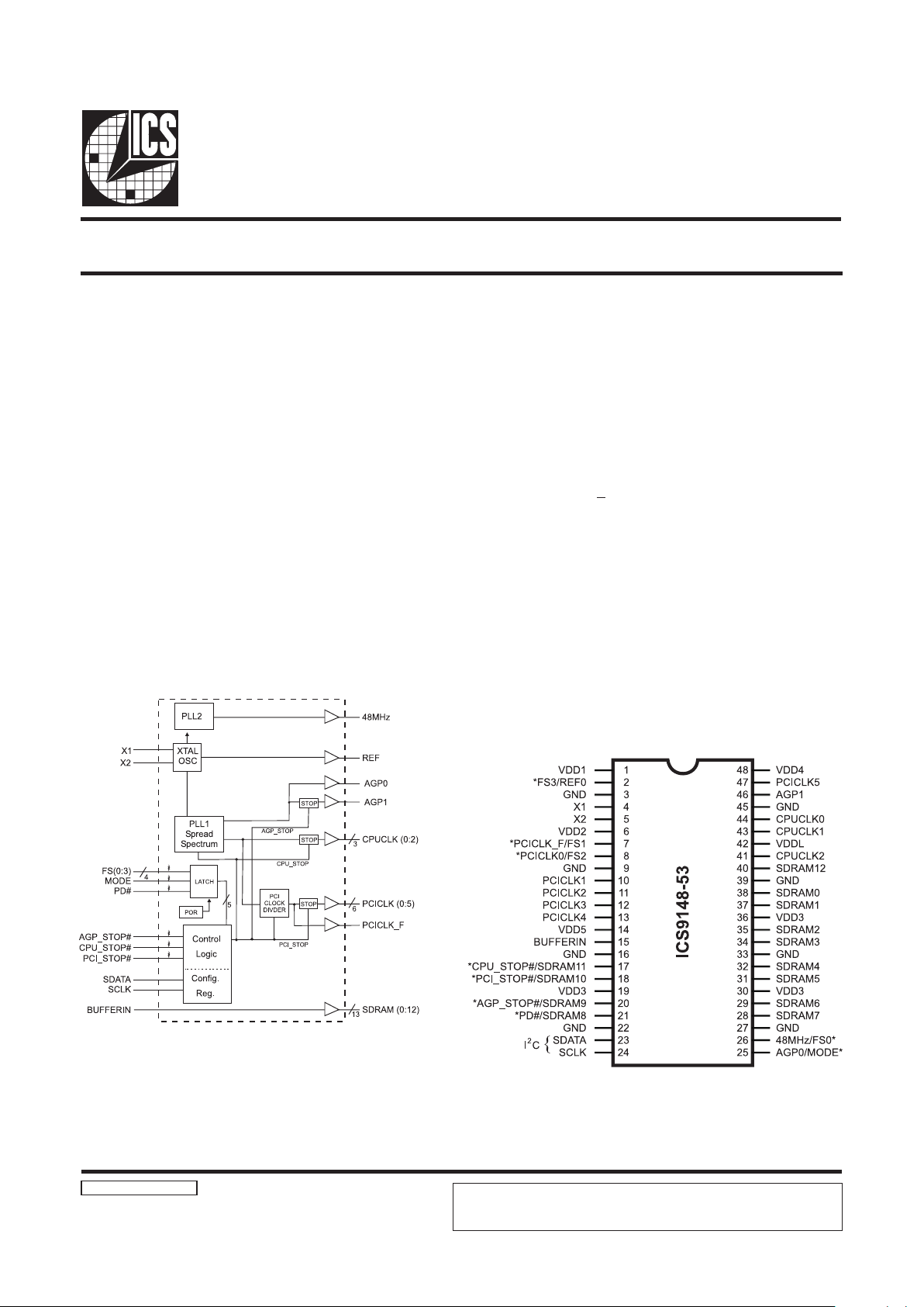
Block Diagram
Pentium is a trademark of Intel Corporation
I2C is a trademark of Philips Corporation
Frequency Generator & Integrated Buffers for Mother Boards
9148-53 Rev C 08/14/98
Pin Configuration
48-Pin SSOP
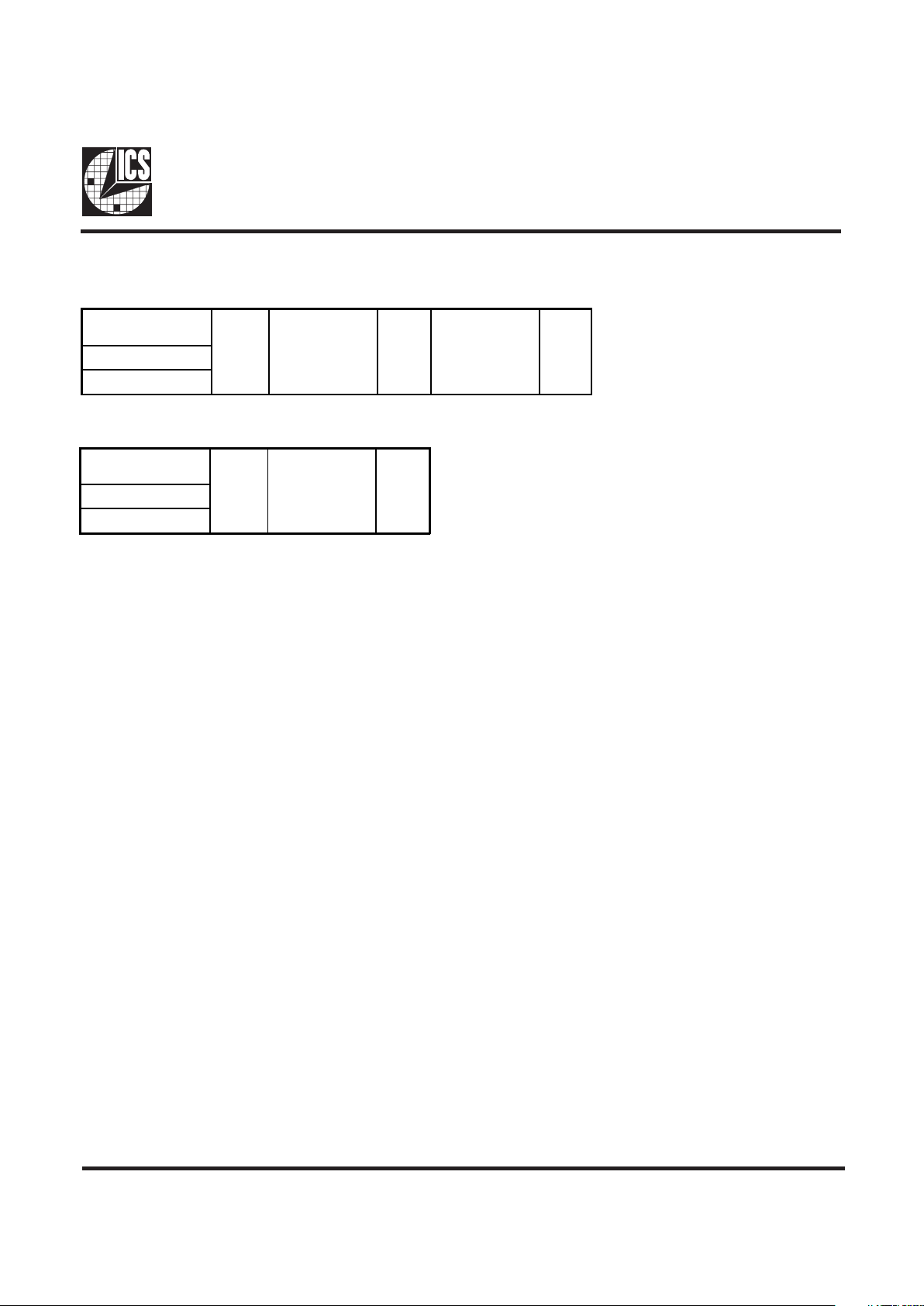
Power Groups
VDD1 = REF (0:1), X1, X2
VDD2 = PCICLK_F, PCICLK(0:5)
VDD3 = SDRAM (0:12), supply for PLL core
VDD4 = AGP (1:2)
VDD5 = Fixed PLL, 48MHz , AGP0
VDDL = CPUCLK (0:3)
* Internal Pull-up Resistor of
240K to 3.3V on indicated inputs
The ICS9148-53 generates all clocks required for high speed
RISC or CISC microprocessor systems such as Intel
PentiumPro, AMD or Cyrix. Sixteen different reference
frequency multiplying factors are externally selectable with
smooth frequency transitions.
Spread spectrum may be enabled through I2C programming.
Spread spectrum typically reduces system EMI by 8dB to
10dB. This simplifies EMI qualification without resorting to
board design iterations or costly shielding. The ICS9148-53
employs a proprietary closed loop design, which tightly
controls the percentage of spreading over process and
temperature variations.
Serial programming I2C interface allows changing functions,
stop clock programming and frequency selection. The
SDRAM12 output may be used as a feed back into an off chip
PLL.
Generates the following system clocks:
- 3 CPU(2.5V/3.3V) up to 150MHz.
- 7 PCI(3.3V) (including one free
running PCICLK)
- 2AGP(3.3V) @ 2 x PCI
- 13 SDRAMs(3.3V) up to 150MHz
- 1 REF (3.3V) @ 14.318MHz
- 1 Fixed clock 3.3V @ 48MHz
Skew characteristics:
- CPU CPU<250ps
- CPU(early) PCI : 1-4ns
Supports Spread Spectrum modulation & I2C
programming for Power Management, Frequency Select
Efficient Power management scheme through power
down CPU, PCI, AGP and CPU_STOP clocks.
Uses external 14.318MHz crystal
48 pin 300mil SSOP.
Read back of FS pin values from I2C
ICS reserves the right to make changes in the device data identified in this
publication without further notice. ICS advises its customers to obtain the latest
version of all device data to verify that any information being relied upon by the
customer is current and accurate.
Page 2
2
ICS9148-53
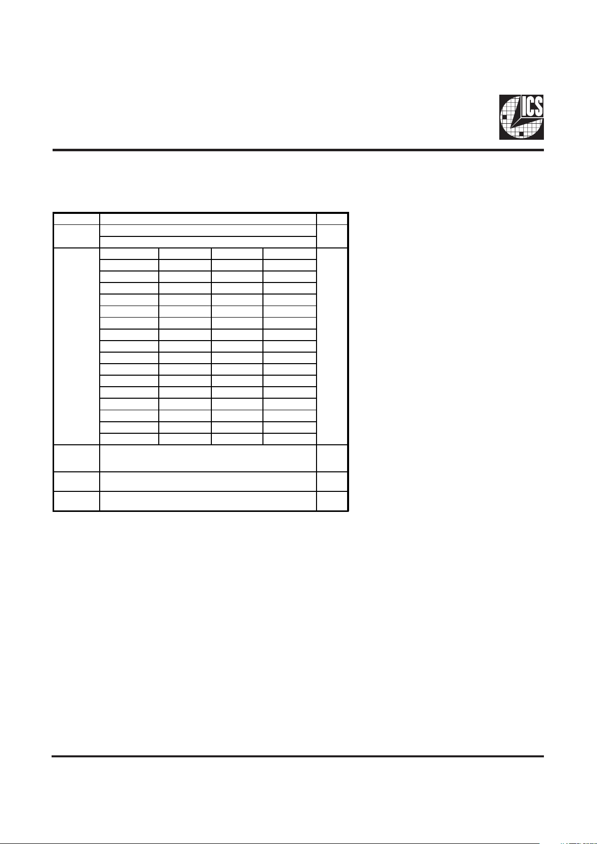
Pin Descriptions
Notes:
1: Internal Pull-up Resistor of 240K to 3.3V on indicated inputs
2: Bidirectional input/output pins, input logic levels are latched at internal power-on-reset. Use 10Kohm resistor to
program logic Hi to VDD or GND for logic low.
PIN NUMBER PIN NAME TYPE DESCRIPTION
1 VDD 1 PW R Ref (0:2), X TAL power supply, nominal 3.3V
2
REF0 OUT 14.318 MHz reference clock.
FS3 IN
Frequency select pin. Latched Input. Along with other FS pins determins the
CPU, SDRAM, PCI & AGP frewuencies.
3,9,16,22,27,
33,39,45
GND PWR Ground
4X1 IN
Crystal input, has internal load cap (33pF) and feedback
resistor from X2
5 X2 OUT
Crystal output, nominally 14.318MHz. Has internal load
cap (33pF)
6 VDD2 PW R Supply for PCICLK_F and PCICLK (0:5), nom inal 3.3V
7
PCICLK_F OUT
Free running PCI clock output. Synchronous with CPUCLKs with 1-4ns skew
(CPU early) This is not affected by PC I_STOP#
FS1
1, 2
IN
Frequency select pin. Latched Input. Along with other FS pins determins the
CPU, SDRAM, PCI & AGP frewuencies.
8
PCICLK0 OU T P CI clock o utputs. Synchrou nous CP UCLKs w ith 1-4ns s kew (CPU early)
FS2
1, 2
IN Frequency select pin. Latched Input
10, 11, 12, 13, 47 PCICLK(1:5) OU T P CI clock o utputs. Synchrou nous CP UCLKs w ith 1-4ns s kew (CPU early)
14 VDD5 PW R Supply for fixed PLL, 48MHz, AGP0
15 BUFFERIN IN Input pin for SDRAM buffers.
17
CPU_STOP# IN
Halts CPUCLK (0:3 ) clocks at log ic 0 level, when input low (in Mobile
Mode, MODE=0)
SDRAM 11 OU T SDRA M clock output
18
PCI_STOP#
1
IN
Halts PCICLK(0:5) clocks at logic 0 level, when input low (In mobile mode,
MODE=0)
SDRAM 10 OU T SDRA M clock output
28, 29, 31, 32, 34,
35,37,38
SDRAM (0:9) OU T SDRAM clock outputs.
20
AGP _STOP #
1
IN
This asynchronous input halts AGP(1:2) clocks at log ic "0" level when input
low (in Mobile Mode, MODE=0) Does not affect AGP0
SDRAM9 OU T SDRAM clock output
21
PD#
1
IN
This asyncheronous Power Down input S tops the V CO, crystal & internal
clocks when active, Low. (In Mobile Mode, MODE =0)
SDRAM8 OU T SDRAM clock output
19,30,36 VDD3 PW R
Supply for SDRAM (0:11), C PU Core, 4 8MHz cloc ks,
nominal 3.3V.
23 SDATA IN Data input for I
2
C serial input.
24 SCLK IN Clock input of I
2
C input
25
AGP0 OUT
Advanced Graphic Port output, powered by VDD4. Not affected by
AGP_S TO P #
MODE
1, 2
IN
Pin 17, 18, 20 & 21 function select pin, 1=Desk top Mode, 0=Mo bile Mode.
Latched Input.
26
48MHz OU T 48MHz output clock for USB timing.
FS0
1, 2
IN
Frequency select pin. Latched Input. Along with other FS pins determins the
CPU, SDRAM, PCI & AGP frewuencies.
41, 43, 44 CPUCLK(0:3) OU T CPU cloc k outputs, powered by VDDL 2. Low if CPU_STOP#=Low
40 SDR AM12 OU T Fe edback SDR AM clock outpu t.
42 VDDL PWR Supply for CPU (0:3), either 2.5V or 3.3V nominal
46 AGP1 OUT Advanced Graphic Port output powered by VDD4.
48 V D D 4 PW R Sup ply for AGP (0:2 )
Page 3
3
ICS9148-53
CPU3.3#_2.5
Input level
(Latch ed Data )
Buffer Selected for
operation at:
12.5V VDD
03.3V VDD
CPU 3.3#_2.5V Buffer selector for CPUCLK drivers.
Power Management Functionality
Mode Pin - Power Management Input Control
MODE, Pin 25
(Latched Input)
Pin 17 Pin 18 Pin 20 Pin 21
0
CPU_STOP#
(INPUT)
PCI_STOP#
(INPUT)
AGP_STOP#
(INPUT)
PD#
(INPUT)
1
SDRAM 11
(OUTPUT)
SDRAM 10
(OUTPUT)
SDRAM 9
(OUTPUT)
SDRAM 8
(OUTPUT)
AGP_STOP# CPU_STOP# PCI_STOP#
AGP,
CPUCLK
Outputs
PCICLK
(0:5)
PCICLK_F,
REF, 48MHz
and SDRAM
Crystal
OSC
VCO AGP(1:2)
1 0 1 Stopped Low Running Running Running Running Running
1 1 1 Running Running Running Running Running Running
1 1 0 Running Stopped Low Running Running Running Running
0 1 1 Running Running Running Running Running Stopped Low
Page 4
4
ICS9148-53
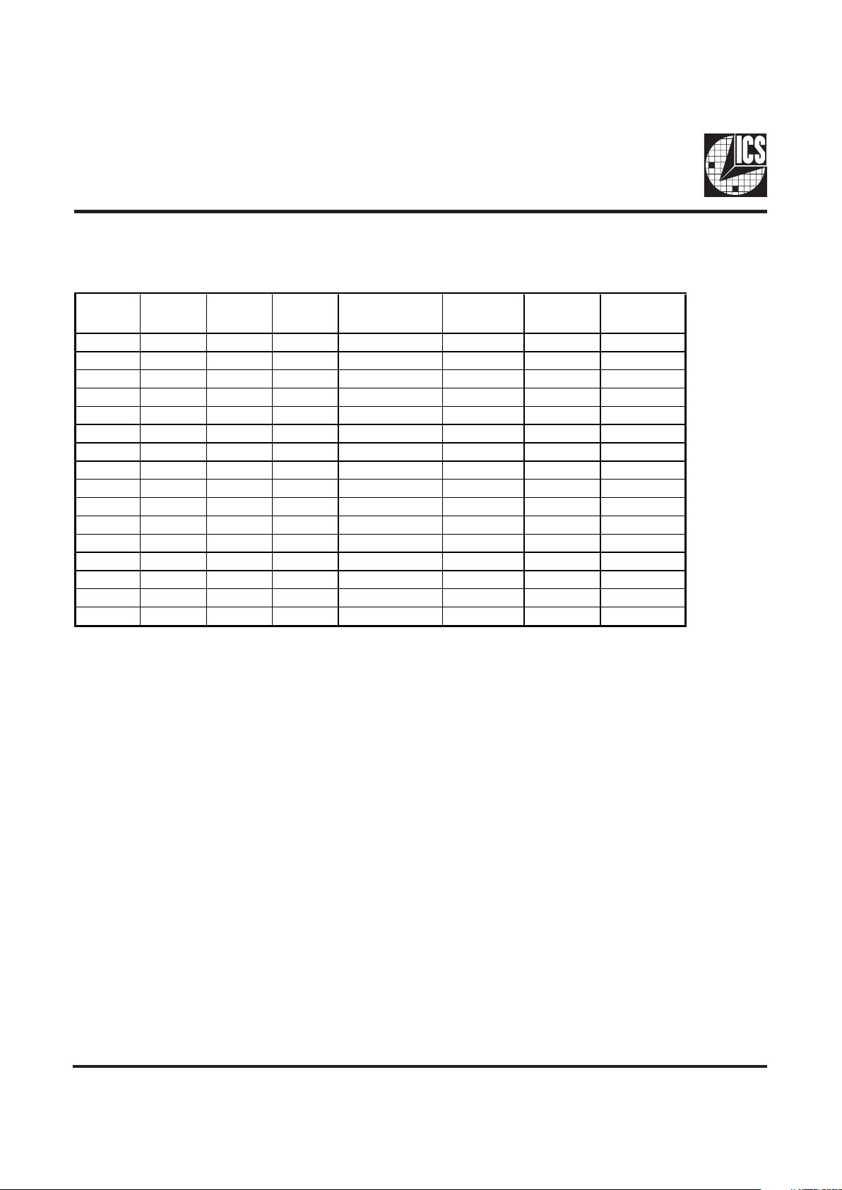
Functionality
VDD1, 2, 3, 4 = 3.3V±5%, TA= 0 to 70°C
Crystal (X1, X2) = 14.31818MHz
FS3 FS2 FS1 FS0
CPU,SDRAM
(MHZ) PCI (MHZ) AGP (M HZ)
REF, IOAPIC
(MHZ)
1111 133 44.3388.6714.318
1110 124 41.3382.6714.318
1101 150 5010014.318
1100 140 46.6793.3314.318
1011 105 35 7014.318
1010 112 37.3374.6714.318
1001 115 38.3376.6614.318
1000 120 40 8014.318
0111 100 33.366.614.318
0110 95.2531.7563.514.318
0101 83.3 33.366.614.318
0100 75 30 6014.318
0011 75 37.57514.318
0010 68.5 34.2568.514.318
0001 66.8 33.466.814.318
0000
60 30 60 14. 318
Page 5
5
ICS9148-53
General I2C serial interface information
A. For the clock generator to be addressed by an I2C controller, the following address must be sent as a start sequence, with
an acknoledge bit between each byte.
B. The clock generator is a slave/receiver I2C component. It can read back the data stored in the latches for verification. (set
R/W# to 1 above) Read-Back will support Intel PIIX4 "Block-Read" protocol, with a "Byte count" following the
address with R/W#=1, then proceding to Byte 0, 1, 2, ...until STOP.
C. The data transfer rate supported by this clock generator is 100K bits/sec (standard mode)
D. The input is operating at 3.3V logic levels.
E. The data byte format is 8 bit bytes.
F. To simplify the clock generator I2C interface, the protocol is set to use only "Block Writes" from the controller. The
bytes must be accessed in sequential order from lowest to highest byte with the ability to stop after any complete byte
has been transferred. The Command code and Byte count shown above must be sent, but the data is ignored for those
two bytes. The data is loaded until a Stop sequence is issued.
G. The Fixed clocks 48MHz and 24MHz are not addressable in the registers for Stopping. These output are always running,
except in Tristate Mode.
H. At power-on, all registers are set to a default condition. Byte 0 defaults to a 0, Bytes 1 through 5 default to a 1
(Enabled output state).
Then Byte 0, 1, 2, etc in
sequence until STOP.
Clock Generator
Address (7 bits)
ACK
+ 8 bits dummy
command code
ACK
+ 8 bits dummy
Byte count
ACK
A(6:0) & R/W#
D2
(H)
Then Byte 0, 1, 2, etc. in
sequence until STOP.
Clock Generat or
Address (7 bits)
ACK
Byte Count
Readback
ACK
A(6:0) & R/W#
D3
(H)
Page 6
6
ICS9148-53
Byte0: Functionality and Frequency Select Register (default = 0)
Serial Configuration Command Bitmap
I2C is a trademark of Philips Corporation
Note 1: Default at power-up will be for latched logic inputs to define frequency;
Bits 2, 6:4 are default to 000
Note: PWD = Power-Up Default
Bit Description PWD
Bit 7
0 - ±0.25% Spread Spectrum Modulation
0
1 - ±0.6% Spread Spectrum Modulation
Bit
(2, 6:4)
Bit (2, 6:4) CPU CLKs PC I CLKs AGP CLKs
Note1
1111 133 44.33 88.67
1110 124 41.33 82.67
1101 150 50 1 00
1100 140 46.67 93.33
1011 105 35 70
1010 112 37.33 74.67
1001 115 38.33 76.66
1000 120 40 80
0111 100 33.33 66.60
0110 9 5.25 3 1.75 63.50
0101 83.3 33.30 66.60
0100 75 30.00 60.00
0011 75 37.50 75.00
0010 68.5 34.25 68.50
0001 66.8 33.40 66.80
0000 60 30.00 60.00
Bit 3
0 - Frequency is selected by hardware select,
Latched Inputs
1 - Frequency is selected by Bit 6:4 (above)
0
Bit 1
0 - Normal
1 - Spread Spectrum Enabled (center spread)
0
Bit 0
0 - Running
1- Tristate all outputs
0
Page 7

7
ICS9148-53
Byte 1: CPU, Active/Inactive Register
(1 = enable, 0 = disable)
Byte 3: SDRAM Active/Inactive Register
(1 = enable, 0 = disable)
Notes:
1. Inactive means outputs are held LOW and are disabled
from switching.
Notes:
1. Inactive means outputs are held LOW and are disabled
from switching.
Notes:
1. Inactive means outputs are held LOW and are disabled
from switching.
B it P in # P WD D e s c ription
Bit 7 - 1 (Reserved)
Bit 6 - 1 (Reserved)
Bit 5 - 1 (Reserved)
Bit 4 4 0 1 SD RA M 1 2 (Ac t/Inac t)
Bit 3 - 1 (Reserved)
Bit 2 41 1 C PU C L K 2 (Ac t/Ina ct)
Bit 1 4 3 1 C P U C L K 1 (Ac t/Ina ct)
Bit 0 4 4 1 C PU C L K 0 (Ac t/Ina ct)
B it Pin # PWD D e s c ription
Bit 7 - 1 (Reserved)
Bit 6 7 1 P C IC L K _ F ( Ac t/Inac t)
Bit 5 - 1 (Reserved)
Bit 4 1 3 1 P C IC LK 4 (A ct/Ina ct)
Bit 3 1 2 1 P C IC LK 3 (A ct/Ina ct)
Bit 2 11 1 P C IC L K 2 (Ac t/Inac t)
Bit 1 1 0 1 P C IC L K 1 (Ac t/Inac t)
Bit 0 8 1 P C IC L K 0 (Ac t/Inac t)
Bit Pin # PWD Description
Bit 7 28 1 SDRAM7 (Act/Inact)
Bit 6 29 1 SDRAM6 (Act/Inact)
Bit 5 31 1 SDRAM5 (Act/Inact)
Bit 4 32 1 SDRAM4 (Act/Inact)
Bit 3 34 1 SDRAM3 (Act/Inact)
Bit 2 35 1 SDRAM2 (Act/Inact)
Bit 1 37 1 SDRAM1 (Act/Inact)
Bit 0 38 1 SDRAM0 (Act/Inact)
Byte 4: SDRAM Active/Inactive Register
(1 = enable, 0 = disable)
Byte 5: Peripheral Active/Inactive Register
(1 = enable, 0 = disable)
Notes:
1. Inactive means outputs are held LOW and are disabled
from switching.
Notes:
1. Inactive means outputs are held LOW and are disabled
from switching.
B it Pin # PW D D es criptio n
Bit 7 25 1 AGP0 (Active/Inactive)
Bit 6 - 1 (Reserved)
Bit 5 26 - FS0#
Bit 4 - 1 (Reserved)
Bit 3 17 1
SDRAM11 (Act/Inact)
(Desktop M ode O nly)
Bit 2 18 1
S DRA M 1 0 (Ac t/Inac t)
(Desktop M ode O nly)
Bit 1 20 1 S D RA M 9 (Ac t/Ina ct)
Bit 0 2 1 1 S DR AM 8 (A ct/I nact)
Bit Pin # PWD Description
Bit 7 - 1 (Reserved)
Bit 6 8 - FS2#
Bit 5 7 - FS1#
Bit 4 47 1 PCICLK5 (Act/Inact)
Bit 3 - 1 (Reserved)
Bit 2 2 - FS3#
Bit 1 46 1 AGP1 (Act/Inact)
Bit 0 2 1 REF0 (Act/Inact)
Byte 2: PCI Active/Inactive Register
(1 = enable, 0 = disable)
Byte 6: Optional Register for Possible
Furture Requirements
Notes:
1. Byte 6 is reserved by Integrated Circuit Systems for futue
applications.
Bit Pin # PWD Description
Bit 7 - 1 (Reserved)
Bit 6 - 1 (Reserved)
Bit 5 - 1 (Reserved)
Bit 4 - 1 (Reserved)
Bit 3 - 1 (Reserved)
Bit 2 - 1 (Reserved)
Bit 1 - 1 (Reserved)
Bit 0 - 1 (Reserved)
Page 8

8
ICS9148-53
CPU_STOP# Timing Diagram
CPU_STOP# is an asychronous input to the clock synthesizer. It is used to turn off the CPU clocks for low power operation.
CPU_STOP# is synchronized by the ICS9148-53. The minimum that the CPU clock is enabled (CPU_STOP# high pulse) is 100
CPU clocks. All other clocks will continue to run while the CPU clocks are disabled. The CPU clocks will always be stopped in
a low state and start in such a manner that guarantees the high pulse width is a full pulse. CPU clock on latency is less than 4
CPU clocks and CPU clock off latency is less than 4 CPU clocks.
Notes:
1. All timing is referenced to the internal CPU clock.
2. CPU_STOP# is an asynchronous input and metastable conditions may exist. This signal is synchronized
to the CPU clocks inside the ICS9148-53.
3. All other clocks continue to run undisturbed. (including SDRAM outputs).
Page 9

9
ICS9148-53
PCI_STOP# Timing Diagram
PCI_STOP# is an asynchronous input to the ICS9148-53. It is used to turn off the PCICLK (0:5) clocks for low power operation.
PCI_STOP# is synchronized by the ICS9148-53 internally. The minimum that the PCICLK (0:5) clocks are enabled (PCI_STOP#
high pulse) is at least 10 PCICLK (0:5) clocks. PCICLK (0:5) clocks are stopped in a low state and started with a full high pulse
width guaranteed. PCICLK (0:5) clock on latency cycles are only one rising PCICLK clock off latency is one PCICLK clock.
Notes:
1. All timing is referenced to the Internal CPUCLK (defined as inside the ICS9148 device.)
2. PCI_STOP# is an asynchronous input, and metastable conditions may exist. This signal is required to be synchronized
inside the ICS9148.
3. All other clocks continue to run undisturbed.
4. CPU_STOP# is shown in a high (true) state.
Page 10

10
ICS9148-53
AGP_STOP# Timing Diagram
AGP_STOP# is an asychronous input to the clock synthesizer. It is used to turn off the AGP (0:1) clocks. for low power
operation. AGP_STOP# is synchronized by the ICS9148-53. The AGP2 clock is free-running and is not affected by AGP_STOP#.
All other clocks will continue to run while the AGPCLKs are disabled. The AGPCLKs will always be stopped in a low state and
start in such a manner that guarantees the high pulse width is a full pulse. AGPCLK on latency is less than AGPCLK and
AGPCLK off latency is less than 4 AGPCLKs. This function is available only with MODE pin latched low.
Notes:
1. All timing is referenced to the internal CPUCLK.
2. AGP_STOP# is an asynchronous input and metastable conditions may exist.
This signal is synchronized to the CPUCLKs inside the ICS9148-53.
3. All other clocks continue to run undisturbed.
4. PD# and PCI_STOP# are shown in a high (true) state.
5. Only applies if MODE pin latched 0 at power up.
Page 11

11
ICS9148-53
Pins 2, 7, 8, 25 and 26 on the ICS9148-53 serve as dual signal
functions to the device. During initial power-up, they act as
input pins. The logic level (voltage) that is present on these
pins at this time is read and stored into a 4-bit internal data
latch. At the end of Power-On reset, (see AC characteristics
for timing values), the device changes the mode of operations
for these pins to an output function. In this mode the pins
produce the specified buffered clocks to external loads.
To program (load) the internal configuration register for these
pins, a resistor is connected to either the VDD (logic 1)
power supply or the GND (logic 0) voltage potential. A 10
Kilohm(10K) resistor is used to provide both the solid CMOS
programming voltage needed during the power-up
programming period and to provide an insignificant load on
the output clock during the subsequent operating period.
Figs. 1 and 2 show the recommended means of implementing
this function. In Fig. 1 either one of the resistors is loaded
onto the board (selective stuffing) to configure the devices
internal logic. Figs. 2a and b provide a single resistor loading
option where either solder spot tabs or a physical jumper
header may be used.
Shared Pin Operation Input/Output Pins
Fig. 1
These figures illustrate the optimal PCB physical layout
options. These configuration resistors are of such a large
ohmic value that they do not effect the low impedance clock
signals. The layouts have been optimized to provide as little
impedance transition to the clock signal as possible, as it
passes through the programming resistor pad(s).
Page 12

12
ICS9148-53
Fig. 2a
Fig. 2b
Page 13

13
ICS9148-53
Absolute Maximum Ratings
Supply Voltage . . . . . . . . . . . . . . . . . . . . . . . . . . . 7.0 V
Logic Inputs . . . . . . . . . . . . . . . . . . . . . . . . . . . . GND 0.5 V to VDD +0.5 V
Ambient Operating Temperature . . . . . . . . . . . . 0°C to +70°C
Storage Temperature . . . . . . . . . . . . . . . . . . . . . . 65°C to +150°C
Stresses above those listed under Absolute Maximum Ratings may cause permanent damage to the device. These ratings are
stress specifications only and functional operation of the device at these or any other conditions above those listed in the
operational sections of the specifications is not implied. Exposure to absolute maximum rating conditions for extended periods
may affect product reliability.
Electrical Characteristics - Input/Supply/Common Output Parameters
TA = 0 - 70C; Supply Voltage VDD = V
DDL
= 3.3 V + /-5% ( unle s s otherwise stated)
PARAMETER SYMBOL CONDITIONS MIN TYP MAX UNITS
Input High Voltage V
IH
2V
DD
+0.3 V
Input L ow Volta ge V
IL
VSS-0.3 0.8 V
Inpu t High Current I
IH
VIN = V
DD
0.1 5
µ
A
Input Low Current I
IL1
VIN = 0 V; Inpu ts with no pull -up re sistors - 5 2.0
µ
A
Input Low Current I
IL2
VIN = 0 V; Inpu ts with pul l -up re sistors -200 -100
µ
A
Operating I
DD3.3OP
CL = 0 pF; 66.8 MHz 100 160 mA
Suppl y C urre nt
Input freque nc y F
i
VDD = 3.3 V; 14.318 M Hz
Input Capacita nce
1
C
IN
Logic Inputs 5 pF
C
INX
X 1 & X2 pins 27 36 45 pF
Tr a nsition Time
1
T
trans
To 1st crossing of t a rget F req. 2 ms
Settling Tim e
1
T
s
From 1s t c ross i ng to 1% targe t Freq. ms
Clk Stabiliza tion
1
T
STAB
From VDD = 3.3 V to 1% tar get Freq. 2 ms
T
CPU-PCI1VT
= 1 .5 V; f = 66/100 MHz; CPU lea ds 1 2.4 4 ns
T
CPU-PCI1VT
= 1 .5 V; f = 83/75 M Hz; CPU lea ds 1 3.8 4 ns
T
AGP-PCI1VT
= 1 .5 V; f = 66.8 MHz; AGP Leads 500 600 ps
T
AGP-PCI1VT
= 1 .5 V; f = 83.3 MHz; AGP Leads 600 700 ps
T
AGP-PCI1VT
= 1 .5 V; f = 100 MHz; AGP Leads
450 550 ps
1
G ua ranteed by de sign, not 100% tested i n production.
Skew
1
Electrical Characteristics - Input/Supply/Common Output Parameters
TA = 0 - 70C; Supply Voltage VDD = 3.3 V +/-5%, V
DDL
= 2.5 V +/-5% (unless other wise stated)
PARAMETER SYMBOL CONDITIONS MIN TYP MAX UNITS
Operating I
DD2.5OP
CL = 0 pF; 66.8 MHz 10 20 mA
Suppl y C urre nt
T
CPU-PCI1VT
= 1 .5 V; f = 66/100 MHz; CPU lea d s 1 2.4 4 ns
T
CPU-PCI1VT
= 1 .5 V; f = 83/75 M Hz; CPU lea ds 1 3.8 4 ns
T
AGP-PCI1VT
= 1 .5 V; f = 66.8 MHz; AGP Leads 500 600 ps
T
AGP-PCI1VT
= 1 .5 V; f = 83.3 MHz; AGP Leads 600 700 ps
T
AGP-PCI1VT
= 1 .5 V; f = 100 MHz; AGP Leads
450 550 ps
Skew
1
Page 14

14
ICS9148-53
Ele ctrical C haracterist ics - CPU
TA = 0 - 70C; VDD = 3.3 V +/-5% , V
DDL
= 2.5 V + /-5%; CL = 10 - 20 pF (unless otherwise stated)
PARAMETER SYMBOL CONDI TI ON S MIN TYP MAX UNITS
Output High Voltage VOH2B I
OH
= -8 mA 2 2.2 V
Output Low Voltage VOL2B I
OL
= 12 mA 0.3 0. 4 V
O utput High Cur rent I OH2B V
OH
= 1 .7 V - 20 -16 mA
Ou tput Low Current I OL2B V
OL
= 0.7 V 19 26 mA
Rise Time
tr2B
1
VOL = 0.4 V, VOH = 2 .0 V 1.5 1. 8 ns
Fall Time
tf2B
1
VOH = 2.0 V, VOL = 0 .4 V 1.6 1. 8 ns
Duty Cycle
dt2B
1
VT = 1.25 V 404755%
Skew
tsk2B
1
VT = 1.25 V 60 250 ps
Jitter, Single E dge
Displacement
2
tjsed2B
1
VT = 1.25 V 200 250 ps
Jitter, One Sigma
tj1s2B
1
VT = 1.25 V 65 150 ps
Jitter, Absolute
tjabs2B
1
VT = 1.25 V
-2 50 160 250 ps
1
G uaranteed by design, not 100% tested in pro duction.
2
Edge d i splacement of a period r elative to a 10-clock-cycle rolling average period.
Ele ctrical C haracterist ics - CPU
TA = 0 - 70C; VDD = V
DDL
= 3.3 V +/-5%; CL = 10 - 20 pF (unless otherwise stated)
PARAMETER SYMBOL CONDI TI ON S MIN TYP MAX UNITS
Output High Voltage V
OH2A
IOH = -28 mA 2.5 2.6 V
Output Low Voltage V
OL2A
IOL = 27 mA 0.35 0.4 V
O utput High Cur rent I
OH2A
VOH = 2 .0 V -29 -23 mA
Ou tput Low Current I
OL2A
VOL = 0.8 V 33 37 mA
Rise Time t
r2A
1
VOL = 0.4 V, VOH = 2 .4 V 1.75 2 ns
Fall Time t
f2A
1
VOH = 2.4 V, VOL = 0.4 V 1.1 2 ns
Duty Cycle d
t2A
1
VT = 1.5 V 455055%
Skew t
sk2A
1
VT = 1.5 V 50 250 ps
Jitter, One Sigma t
j1s2A
1
VT = 1.5 V 65 150 ps
Jitter, Absolute
t
jabs2A
1
VT = 1.5 V
-2 50 165 250 ps
1
G ua ranteed by d e sign, not 100% tested i n production.
Page 15

15
ICS9148-53
Ele ctrical C haracterist ics - SDRA M
TA = 0 - 70C; VDD = V
DDL
= 3.3 V +/-5%; CL = 30 pF
PARAMETER SY MBOL CONDITIONS MIN TYP MAX UNITS
O utput Hi gh Voltage V
OH1
IOH = -28 mA 2 .4 3 V
Output Low Voltage V
OL1
IOL = 23 mA 0.2 0.4 V
Ou tput Hi gh Cur rent I
OH1
VOH = 2.0 V -60 -40 mA
Output Low Current I
OL1
VOL = 0.8 V 41 50 mA
Rise Time
1
T
r1
VOL = 0.4 V, VOH = 2.4 V 1.75 2 ns
Fall Time
1
T
f1
VOH = 2.4 V , VOL = 0.4 V 1.5 2 ns
Duty Cycle
1
D
t1
VT = 1.5 V 45 50 55 %
Propagation Delay T
prop
VT = 1.5 V 4 .2 6 ns
Skew
1
T
sk1
VT = 1.5 V
200 500 ps
1
Guaranteed by design, not 100% tested in pr odu c t ion.
Ele ctrical C haracterist ics - PCI
TA = 0 - 70C; VDD = V
DDL
= 3.3 V +/-5%; CL = 30 p F (unless otherwise stated)
PARAMETER SYMBOL CONDI TI ON S MIN TYP MAX UNITS
Output High Voltage V
OH1
IOH = -28 mA 2.4 3 V
Output Low Voltage V
OL1
IOL = 23 mA 0.2 0. 4 V
O utput High Cur rent I
OH1
VOH = 2 .0 V -60 -40 mA
Ou tput Low Current I
OL1
VOL = 0.8 V 41 50 mA
Rise Time t
r1
1
VOL = 0.4 V, VOH = 2.4 V 1.8 2 ns
Fall Time t
f1
1
VOH = 2.4 V, VOL = 0.4 V 1.6 2 ns
Duty Cycle d
t1
1
VT = 1.5 V 455155%
Skew t
sk1
1
VT = 1.5 V 130 250 ps
Jitter, One Si gma
1
t
j1s1a
VT = 1.5 V, synchronous 4 0 150 ps
t
j1s1b
VT = 1.5 V, asynch ronous 200 250 ps
Jitter, Absolute
1
tab
s1a
VT = 1.5 V, synchronous -25 0 135 250 ps
t
jabs1b
VT = 1.5 V, asynch ronous
-650 500 650 ps
1
G ua ranteed by d e sign, not 100% tested i n production.
Page 16

16
ICS9148-53
Ele ctrical C haracterist ics - AGP
TA = 0 - 70C; VDD = V
DDL
= 3.3 V +/-5%; CL = 30 p F (unless otherwise stated)
PARAMETER SYMBOL CONDI TI ON S MIN TYP MAX UNITS
Output High Voltage V
OH1
IOH = -28 mA 2. 4 3 V
Output Low Voltage V
OL1
IOL = 23 mA 0.2 0. 4 V
O utput High Cur rent I
OH1
VOH = 2 .0 V -60 -40 mA
Ou tput Low Current I
OL1
VOL = 0.8 V 41 50 mA
Rise Time t
r1
1
VOL = 0.4 V, VOH = 2.4 V 1.1 2 ns
Fall Time t
f1
1
VOH = 2.4 V, VOL = 0.4 V 1 2 ns
Duty Cycle d
t1
1
VT = 1.4 V 454955%
Skew t
sk1
1
VT = 1.5 V 130 250 ps
Jitter, One Si gma
1
t
j1s1
VT = 1.5 V 2 3 %
Jitter, Absolute
1
t
abs1a
VT = 1.5 V, synchronous -5 2. 5 5 %
t
jabs1b
VT = 1.5 V, asynch ronous
-6 4.5 6 %
1
G ua ranteed by d e sign, not 100% tested i n production.
Elect rical C haracterist i cs - 48MH z, REF0
TA = 0 - 70C; VDD = V
DDL
= 3.3 V +/-5%; CL = 10 -20 pF ( unle s s otherwis e s ta ted)
PARA METER SYMBOL COND ITIO NS MIN TYP MAX U NITS
Output High Voltage V
OH5
IOH = -16 mA 2.4 2.6 V
Output Low Voltage V
OL5
IOL = 9 mA 0.3 0.4 V
O utput High Curr e nt I
OH5
VOH = 2 . 0 V - 32 -22 mA
O utput Low C urrent I
OL5
VOL = 0. 8 V 16 25 mA
Rise Time t
r5
1
VOL = 0. 4 V, VOH = 2.4 V 2 4 ns
F all Time t
f5
1
VOH = 2.4 V, VOL = 0.4 V 1.9 4 ns
Duty Cycle d
t5
1
VT = 1.5 V 455457%
Jitte r , One Sigma t
j1s5
1
VT = 1. 5 V 1 3 %
Jitter, Absolute
t
jabs5
1
VT = 1. 5 V
-5 - 5 %
1
G ua r a nte ed by de s ign, not 100% tes te d in production.
Page 17

17
ICS9148-53
General Layout Precautions:
1) Use a ground plane on the top layer
of the PCB in all areas not used by
traces.
2) Make all power traces and vias as
wide as possible to lower inductance.
Notes:
1 All clock outputs should have series
terminating resistor. Not shown in all
places to improve readibility of
diagram
2 Optional EMI capacitor should be
used on all CPU, SDRAM, and PCI
outputs.
3 Optional crystal load capacitors are
recommended.
Capacitor Values:
C1, C2 : Crystal load values determined by user
C3 : 100pF ceramic
All unmarked capacitors are 0.01µF ceramic
Page 18

18
ICS9148-53
48 pin SSOP Package
Ordering Information
ICS9148F-53
Pattern Number (2 or 3 digit number for parts with ROM code patterns)
Package Type
F=SSOP
Device Type (consists of 3 or 4 digit numbers)
Prefix
ICS, AV = Standard Device
Example:
ICS XXXX F - PPP
SYMBOL COMM ON DIMENSIONS VAR I ATIO N S D N
MIN. NOM. MAX . MIN. NOM. MAX.
A .095 .101 .110 AC .620 .625 .630 48
A1 .008 .012 .016
A2 .088 .090 .092
B .008 .010 .0135
C.005- .010
D See Variations
E .292 .2 96 .299
e0.025 BSC
H .400 .406 .410
h .010 .013 .016
L .024 .032 .040
N See Variations
∝
0° 5° 8°
X .085 .093 .100
ICS reserves the right to make changes in the device data identified in this
publication without further notice. ICS advises its customers to obtain the latest
version of all device data to verify that any information being relied upon by the
customer is current and accurate.
 Loading...