

Page 1
Integrated
Circuit
Systems, Inc.
General Description Features
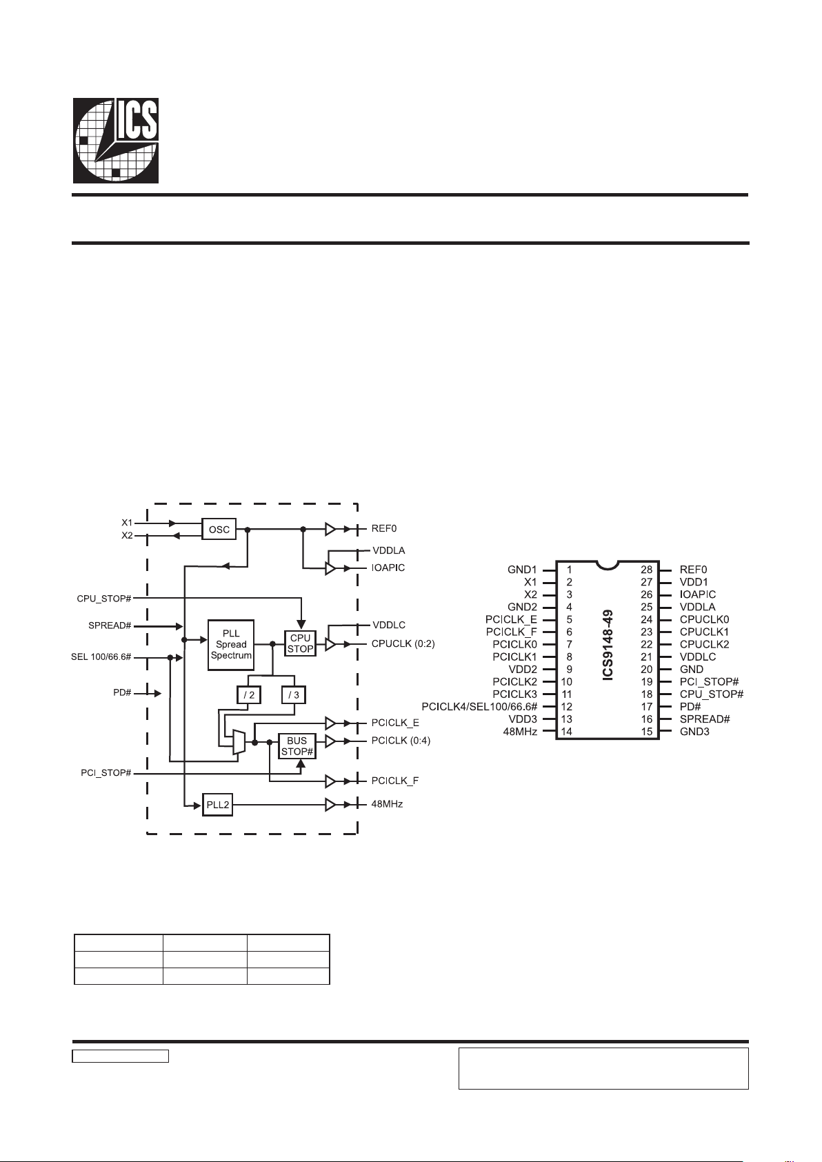
ICS9148-49
Block Diagram
Pentium/ProTM System Clock Chip
9148-49 Rev D 1/12/99
Pin Configuration
28-pin SSOP (209mil body)
Pentium is a trademark on Intel Corporation.
3CPUs @2.5V, up to 100MHz.
7PCIs @3.3V(including 1 free running, 1 Early).
1-48MHz(@3.3V) fixed.
1 REF(3.3V, 14.318MHz), 1 IOAPIC(2.5V, 14.318MHz)
Strong REF clock (1V/ns @ 50pf load)
Excellent power management features including Power
down, PCI and CPU stops
Spread Spectrum for EMI control(0.5% down spread)
Early PCI (3.0ns ±250ps)
The ICS9148-49 is part of a reduced pin count two-chip clock
solution for designs using an Intel BX style chipset.
Companion SDRAM buffers are ICS9179-03, -04 and -12.
There are two PLLs, with the first PLL capable of spread
spectrum operation. Spread spectrum typically reduces system
EMI by 8-10dB. The second PLL provides support for USB
48MHz requirements. CPU frequencies up to 100MHz are
supported.
Ground Groups
GND1=REF0, X1, PLL CORE, X2, IOAPIC
GND2=PCICLK_E, PCICLK_F, PCICLK(04)
GND=CPUCLK
GND3 = 48MHz
Power Groups
VDD1=REF0, X1, X2
VDD2=PCICLK_E , PCICLK_F , PCICLK(0:4)
VDD3=48MHz
VDDLC=CPUCLK(0:2)
VDDLA=IOAPIC
#6.66/001LES
zHMUPCzHMICP
10013.33
06.663.33
Frequency Table:
ICS reserves the right to make changes in the device data identified in
this publication without further notice. ICS advises its customers to
obtain the latest version of all device data to verify that any
information being relied upon by the customer is current and accurate.
Page 2
2
ICS9148-49
Pin Descriptions
REBMUNNIPEMANNIPEPYTNOITPIRCSED
11DNGRWP.2X,1X,stuptuoFERrofdnuorG
21XNI
daolFp33lanretnisah,tupnilatsyrCzHM813.41NI_LATX
2Xmorfrotsiserkcabdeefdnapac
32XTUOFp33pacdaollanretnisah,tuptuolatsyrCTUO_LATX
42DNGRWPstuptuoICProfdnuorG
5E_KLCICPTUO
toN.sp052±sn2yb)F_,4:0(KLCICPsdaeL.KLCICPylraE
#POTS_ICPybdetceffa
6F_KLCICPTUO#POTS_ICPybdetceffatoNo.tuptuoICPgninnuReerF
11,01,8,7)3:0(KLCICPTUOV3.3elbitapmocLTT.stuptuokcolcICP
92DDVRWPV3.3yllanimon,stuptuoKLCICProfrewoP
21
4_KLCICPTUOV3.3elbitapmocLTT.tuptuokcolcICP
#6.66/001LESNI
zHM6.66rozHM001gnilbanerofniptceleS
)zHM3.33suonorhcnyssyawlaICP(zHM6.66=L,zHM001=H
313DDVRWPzHM84rofrewoP
41zHM84TUOzHM84@tuptuoKLCdexiF
513DNGRWPzHM84rofdnuorG
61#DAERPSNI1.daerpsnwod%5.0.evitcanehwmurtcpSdaerpSnosnruT
71#DPNI.ffodenruteratuptuolla,sLLPlanretnI.pihcnwodsrewoP
81#POTS_UPCNI.wolsitupninehwlevel"0"cigolta)0:2(KLCUPCtlaH
91#POTS_ICPNI
seoD.woltupninehwlevel"0"cigolta)4:0(KLCICPstlaH
F_KLCICP7E_KLCICPtceffaton
02DNGRWPerocLLProfdnuorG
12CLDDVRWPV5.2yllanimon,stuptuoUPCrofrewoP
42,32,22)0:2(KLCUPCTUOV5.2yllanimonstuptuokcolctsoHdnaUPC
62CIPAOITUO.zHM813.41tuptuokcolcCIPAOI
52ALDDVRWPCIPAOIrofrewoP
721DDVRWP.stuptuoFERrofrewoP
820FERTUO.purewoptatupnidehctaL/tuptuokcolczHM813.41
Page 3
3
ICS9148-49
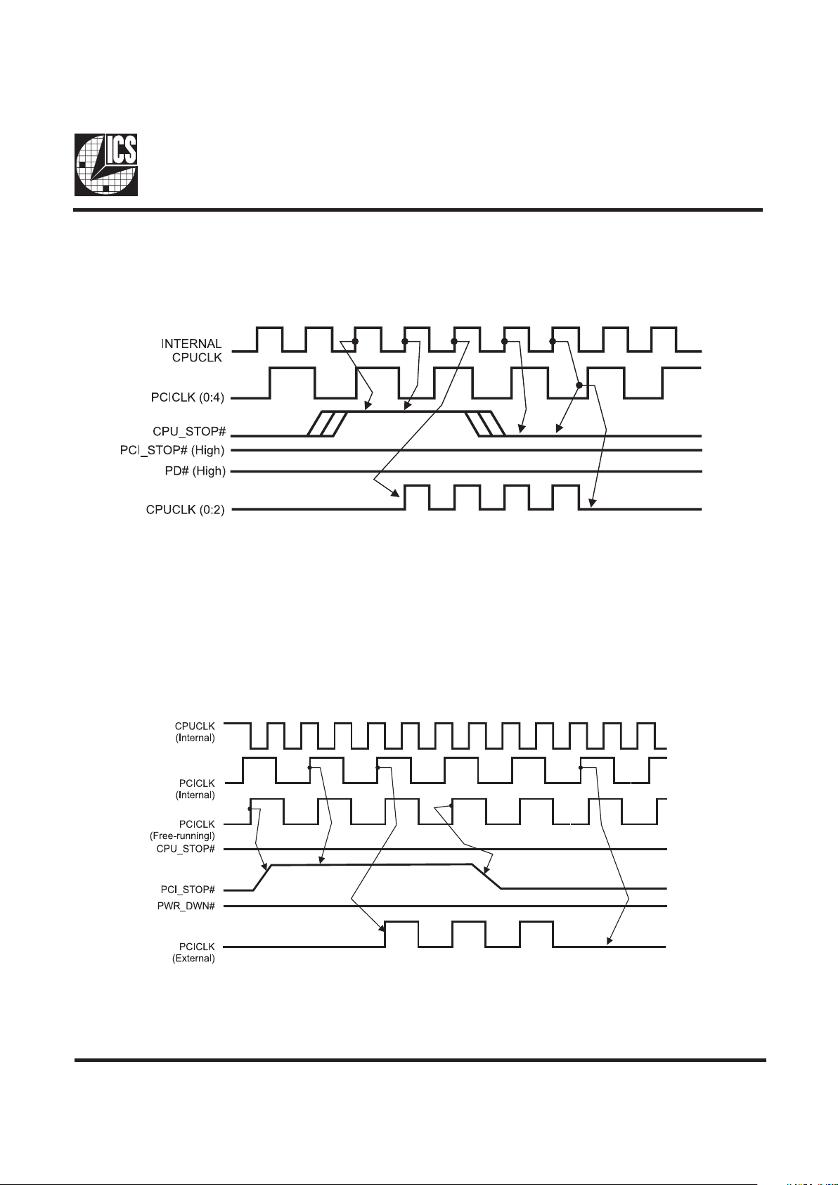
PCI_STOP# Timing Diagram
PCI_STOP# is an asynchronous input to the ICS9148-49. It is used to turn off the PCICLK (0:5) clocks for low power operation.
PCI_STOP# is synchronized by the ICS9148-49 internally. PCICLK (0:5) clocks are stopped in a low state and started with a full
high pulse width guaranteed. PCICLK (0:5) clock on latency cycles are only one rising PCICLK clock off latency is one PCICLK
clock.
CPU_STOP# Timing Diagram
CPUS_TOP# is an asychronous input to the clock synthesizer. It is used to turn off the CPUCLKs for low power operation.
CPU_STOP# is synchronized by the ICS9148-49. All other clocks will continue to run while the CPUCLKs clocks are disabled.
The CPUCLKs will always be stopped in a low state and start in such a manner that guarantees the high pulse width is a full
pulse. CPUCLK on latency is less than 4 CPUCLKs and CPUCLK off latency is less than 4 CPUCLKs.
Notes:
1. All timing is referenced to the internal CPUCLK.
2. CPU_STOP# is an asynchronous input and metastable conditions may exist.
This signal is synchronized to the CPUCLKs inside the ICS9148-49.
3. All other clocks continue to run undisturbed including SDRAMR.
4. PD# and PCI_STOP# are shown in a high (true) state.
Notes:
1. All timing is referenced to the Internal CPUCLK (defined as inside the ICS9148 device.)
2. PCI_STOP# is an asynchronous input, and metastable conditions may exist. This signal is required to be synchronized
inside the ICS9148.
3. All other clocks continue to run undisturbed.
4. PD# and CPU_STOP# are shown in a high (true) state.
Page 4

4
ICS9148-49
PD# Timing Diagram
The power down selection is used to put the part into a very low power state without turning off the power to the part. PD# is
an asynchronous active low input. This signal is synchronized internal by the ICS9148-49 prior to its control action of
powering down the clock synthesizer. Internal clocks will not be running after the device is put in power down state. When PD#
is active (low) all clocks are driven to a low state and held prior to turning off the VCOs and the Crystal oscillator. The power on
latency is guaranteed to be less than 3mS. The power down latency is less than three CPUCLK cycles. PCI_STOP# and
CPU_STOP# are dont care signals during the power down operations.
Notes:
1. All timing is referenced to the Internal CPUCLK (defined as inside the ICS9148 device).
2. PD# is an asynchronous input and metastable conditions may exist. This signal is synchronized inside the ICS9148.
3. The shaded sections on the VCO and the Crystal signals indicate an active clock is being generated.
Page 5

5
ICS9148-49
Absolute Maximum Ratings
Supply Voltage . . . . . . . . . . . . . . . . . . . . . . . . . . . 7.0 V
Logic Inputs . . . . . . . . . . . . . . . . . . . . . . . . . . . . GND 0.5 V to VDD +0.5 V
Ambient Operating Temperature . . . . . . . . . . . . 0°C to +70°C
Storage Temperature . . . . . . . . . . . . . . . . . . . . . . 65°C to +150°C
Stresses above those listed under Absolute Maximum Ratings may cause permanent damage to the device. These ratings are
stress specifications only and functional operation of the device at these or any other conditions above those listed in the
operational sections of the specifications is not implied. Exposure to absolute maximum rating conditions for extended periods
may affect product reliability.
Electrical Characteristics - Input/Supply/Common Output Parameters
TA = 0 - 70C; Supply Voltage VDD = V
DDL
= 3.3 V +/-5% (unless otherwise stated)
PARAMETER SYMBOL CONDITIONS MIN TYP MAX UNITS
Input High Voltage V
IH
2V
DD
+0.3 V
Input Low Voltag e V
IL
VSS-0.3 0.8 V
Input High Current I
IH
VIN = V
DD
0.1 5
µ
A
Input Low Current I
IL1
VIN = 0 V; Inputs with no pull-up resistors -5 2.0
µ
A
Input Low Current I
IL2
VIN = 0 V; Inputs with pull-up resistors -200 -100
µ
A
Operating C
L
= 0 pF; 66.6 MHz 70 100
Supply Current C
L
= 0 pF; 100 MHz 75 100
Input frequency F
i
VDD = 3.3 V; 12 14.318 16 MHz
C
IN
Logic Inputs 5 pF
C
INX
X1 & X2 pins 27 36 45 pF
Transition Time
1
T
trans
To 1st crossing of target Freq. 3 m s
Settling Time
1
T
s
From 1st crossing to 1% target Freq. 2 m s
Clk Stabilization
1
T
STAB
From VDD = 3.3 V to 1% target Freq.
3ms
1
Guaranteed by design, not 100% tested in production.
I
DD3.3OP
mA
Input Capacitance
1
Electrical Characteristics - Input/Supply/Common Output Parameters
TA = 0 - 70C; Supply Voltage VDD = 3.3 V +/-5%, V
DDL
= 2.5 V +/-5% (unless otherwise stated)
PARAMETER SYMBOL CONDITIONS MIN TYP MAX UNITS
C
L
= 0 pF; 66.8 MHz 17 50
C
L
= 0 pF;133 MHz 27 50
Power Down Current
I
DD2.5OPD
5 100 µ
A
T
CPU-PCI(F,0:4)VT
= 1.5 V / 1.25V; CPU leads 1.5 3 4 ns
T
CPU-PCI(E)
VT = 1.5 V / 1.25V; PCI leads 180 200 250 ps
1
Guaranteed by design, not 100% tested in production.
I
DD2.5OP
mA
Skew
1
Operating Supply
Current
Page 6

6
ICS9148-49
Electrical Characteristics - CPU
TA = 0 - 70C; VDD = 3.3 V +/-5%, V
DDL
= 2.5 V +/-5%; CL = 10 - 20 pF (unless otherwise stated)
PARAMETER SYMBOL CONDITIONS MIN TYP MAX UNITS
Output High Voltage VOH2B I
OH
= -12 mA 2 2.2 V
Output Low Voltage VOL2B I
OL
= 12 mA 0.3 0.4 V
Output High Current IO H2B V
OH
= 1.7 V -20 -16 mA
Output Low Current IOL2B V
OL
= 0.7 V 19 26 mA
Rise Time
tr2B
1
VOL = 0.4 V, VOH = 2.0 V 1.2 1.6 ns
Fall Time
tf2B
1
VOH = 2.0 V, VOL = 0.4 V 1.2 1.6 ns
Duty Cycle
dt2B
1
VT = 1.25 V 45 50 55 %
Skew
tsk2B
1
VT = 1.25 V 60 175 ps
Jitter, Single Edge
Dis
p
lacement
2
tjsed2B
1
VT = 1.25 V
200 250 ps
Jitter, One Sigma
tj1s2B
1
VT = 1.25 V 65 150 ps
Jitter, Absolute
tjabs2B
1
VT = 1.25 V
-300 160 300 ps
1
Guaranteed by design, not 100% tested in production.
2
Edge displacement of a period relative to a 10-clock-cycle rolling average period.
Electrical Characteristics - PCI
TA = 0 - 70C; VDD = V
DDL
= 3.3 V +/-10%; CL = 30 pF (unless otherwise stated)
PARAMETER SYMBOL CONDITIONS MIN TYP MAX UNITS
Output High Voltage V
OH1
IOH = -11 mA 2.6 3 V
Output Low Voltage V
OL1
IOL = 9.4 mA 0.2 0.4 V
Output High Current I
OH1
VOH = 2.0 V -30 -22 mA
Output Low Current I
OL1
VOL = 0.8 V 16 25 mA
Rise Time t
r1
1
VOL = 0.4 V, VOH = 2.4 V 1.7 2 ns
Fall Time t
f1
1
VOH = 2.4 V, VOL = 0.4 V 1.6 2 ns
Duty Cycle d
t1
1
VT = 1.5 V 45 51 55 %
Skew t
sk1
1
VT = 1.5 V 200 500 ps
Jitter, Single Edge
Dis
p
lacement
2
tjsed2B
1
VT = 1.25 V
200 500 ps
tab
s1a
VT = 1.5 V 200 ps
t
jabs1b
VT = 1.5 V
-250 250 ps
1
Guaranteed by design, not 100% tested in production.
Jitter, Absolute
1
Page 7

7
ICS9148-49
Electrical Characteristics - REF0
TA = 0 - 70C; VDD = V
DDL
= 3.3 V +/-10%; CL = 50 pF (unless otherwise stated)
PARAMETER SYMBOL CONDITIONS MIN TYP MAX UNITS
Output High Voltage V
OH5
IOH = -12 mA 2. 6 2. 7 V
Output Low Voltage V
OL5
IOL = 9 mA 0.3 0.4 V
Output High Current I
OH5
VOH = 2.0 V -32 -22 mA
Output Low Current I
OL5
VOL = 0.8 V 16 25 mA
Rise Time t
r5
1
VOL = 0.4 V, VOH = 2.4 V 1.2 2 ns
Fall Time t
f5
1
VOH = 2.4 V, VOL = 0.4 V 1.1 2 ns
Duty Cycle d
t5
1
VT = 1.5 V 53 54 55 %
Jitter, One Sigma t
j
1s5
1
VT = 1.5 V 1 3 %
Jitter, Absolute
t
jabs5
1
VT = 1.5 V
-5 - 5 %
1
Guaranteed by design, not 100% tested in production.
Electrical Characteristics - IOAPIC
TA = 0 - 70C; VDD = V
DDL
= 3.3 V +/-10%; CL = 20 pF (unless otherwise stated)
PARAMETER SYMBOL CONDITIONS MIN TYP MAX UNITS
Output High Voltage VOH2B I
OH
= -12 mA 2 2.2 V
Output Low Voltage VOL2B I
OL
= 12 mA 0.3 0.4 V
Output High Current IOH2B V
OH
= 1.7 V -20 -16 mA
Output Low Current IOL2B V
OL
= 0.7 V 19 26 mA
Rise Time
tr2B
1
VOL = 0.4 V, VOH = 2.0 V 1. 2 1.6 ns
Fall Time
tf2B
1
VOH = 2.0 V, VOL = 0.4 V 1. 2 1.6 ns
Duty Cycle
dt2B
1
VT = 1.25 V 45 50 55 %
Jitter, One Sigma
1
t
j
1s1
VT = 1.5 V 2 3 %
Jitter, Absolute1
t
jabs1b
VT = 1.5 V
-6 4.5 6 %
1
Guaranteed by design, not 100% tested in production.
Electrical Characteristics - 48M
TA = 0 - 70C; VDD = V
DDL
= 3.3 V +/-5%; CL = 20 pF
PARAMETER SYMBOL CONDITIONS MIN TYP MAX UNITS
Output High Voltage V
OH1
IOH = -11 mA 2.4 3 V
Output Low Voltage V
OL1
IOL = 9.4 mA 0.2 0.4 V
Output High Current I
OH1
VOH = 2.0 V -22 -18 mA
Output Low Current I
OL1
VOL = 0.8 V 12 20 mA
Rise Time t
r1
1
VOL = 0.4 V, VOH = 2.4 V 2.2 2.5 ns
Fall Time t
f1
1
VOH = 2.4 V, VOL = 0.4 V 1.9 2.5 ns
Duty Cycle
1
D
t1
VT = 1.5 V 45 50 55 %
Jitter, One Sigma
1
T
j
1s1
VT = 1.5 V 2 3 %
Jitter, Absolute
1
T
jabs1
VT = 1.5 V
-6 4.5 6 %
1
Guaranteed by design, not 100% tested in production.
Page 8

8
ICS9148-49
General Layout Precautions:
1) Use a ground plane on the top layer
of the PCB in all areas not used by
traces.
2) Make all power traces and vias as
wide as possible to lower inductance.
Notes:
1 All clock outputs should have series
terminating resistor. Not shown in all
places to improve readibility of
diagram
2 Optional EMI capacitor should be
used on all CPU, SDRAM, and PCI
outputs.
3 Optional crystal load capacitors are
recommended.
Capacitor Values:
C1, C2 : Crystal load values determined by user
C3 : 100pF ceramic
All unmarked capacitors are 0.01µF ceramic
Page 9

9
ICS9148-49
Ordering Information
ICS9148F-49
Pattern Number (2 or 3 digit number for parts with ROM code patterns)
Package Type
F=SSOP
Device Type (consists of 3 or 4 digit numbers)
Prefix
ICS, AV = Standard Device
Example:
ICS XXXX F - PPP
LOBMYS
NOMMOC
SNOISNEMID
SNOITAIRAV
D
.NIM.MON.XAMN .NIM.MON.XAM
A860.0370.0870.041932.0442.0942.0
1A200.0500.0800.061932.0442.0942.0
2A660.0860.0070.002872.0482.0982.0
b010.0210.0510.042813.0323.0823.0
c400.0600.0800.082793.0204.0704.0
DsnoitairaVeeS03793.0204.0704.0
E502.0902.0212.0
eCSB6520.0
H103.0703.0113.0
L520.0030.0730.0
NsnoitairaVeeS
∝
°0°4°8
Dimensions in inches
28 Pin SSOP Package
ICS reserves the right to make changes in the device data identified in
this publication without further notice. ICS advises its customers to
obtain the latest version of all device data to verify that any
information being relied upon by the customer is current and accurate.
 Loading...