

Page 1
Integrated
Circuit
Systems, Inc.
General Description Features
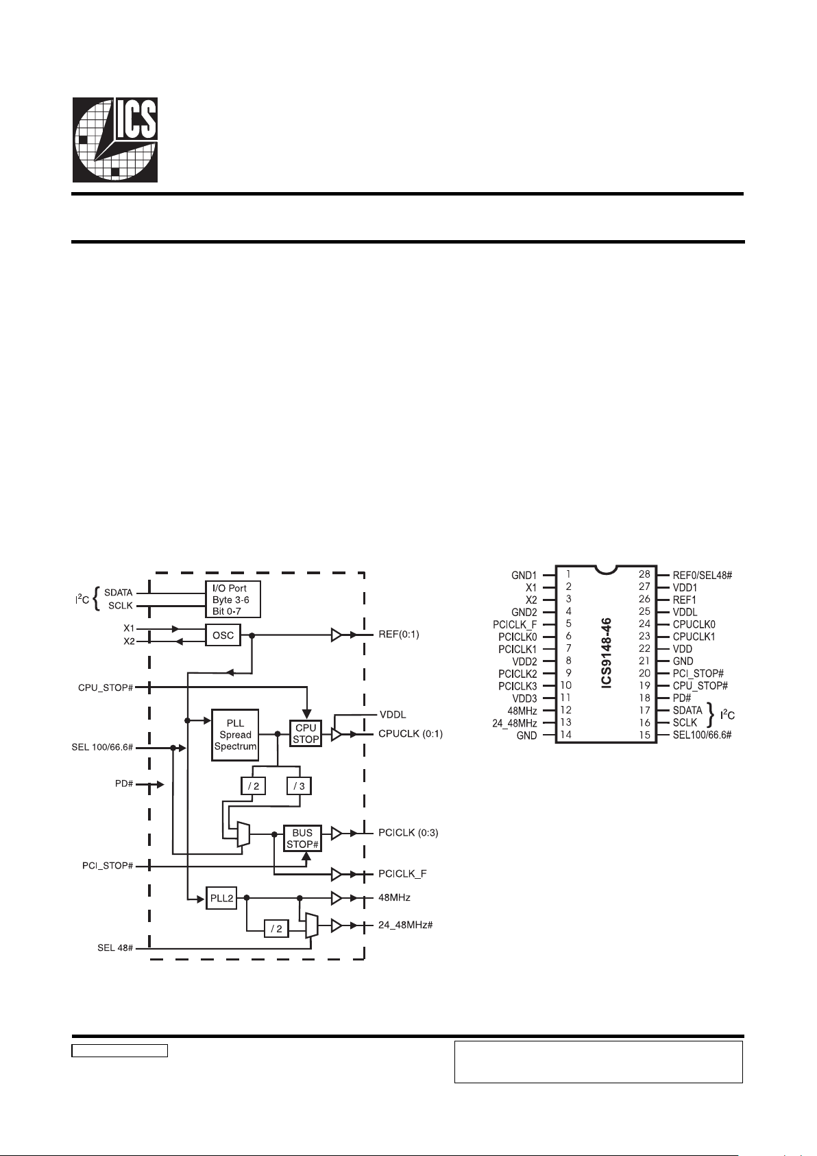
ICS9148-46
Block Diagram
Pentium/ProTM System Clock Chip
9148-46 Rev E 4/20/99
Pin Configuration
28 pin SSOP
Pentium is a trademark on Intel Corporation.
Generates system clocks for CPU, PCI, 14.314 MHz,
48 and 24MHz.
Supports single or dual processor systems
Skew from CPU (earlier) to PCI clock 1 to 4ns
Separate 2.5V and 3.3V supply pins
2.5V outputs: CPU
3.3V outputs: PCI, REF
No power supply sequence requirements
28 pin SSOP
Spread Sectrum operation optional for PLL1
CPU frequencies to 100MHz are supported.
The ICS9148-46 is part of a reduced pin count two-chip clock
solution for designs using an Intel BX style chipset.
Companion SDRAM buffers are ICS9179-03, and -12.
There are two PLLs, with the first PLL capable of spread
spectrum operation. Spread spectrum typically reduces system
EMI by 8-10dB. The second PLL provides support for USB
(48MHz) and 24MHz requirements. CPU frequencies up to
100MHz are supported.
The I2C interface allows stop clock programming, frequency
selection, and spread spectrum operation to be programmed.
Clock outputs include two CPU (2.5V or 3.3V), five PCI (3.3V),
two REF (3.3V), one 48MHz, and one selectable 48_24MHz.
Ground Groups
GND = Ground Source Core, CPUCLK (0:1)
GND1 = REF(0:1), X1, X2
GND2 = PCICLK_F, PCICLK (0:5)
GND3=48MHz, 24/48MHz
Power Groups
VDD = Supply for PLL core
VDD1 = REF(0:1), X1, X2
VDD2 = PCICLK_F, PCICLK (0:3)
VDD3 = 48MHz, 24/48MHz
VDDL = CPUCLK (0:1)
ICS reserves the right to make changes in the device data identified in
this publication without further notice. ICS advises its customers to
obtain the latest version of all device data to verify that any
information being relied upon by the customer is current and accurate.
Page 2
2
ICS9148-46
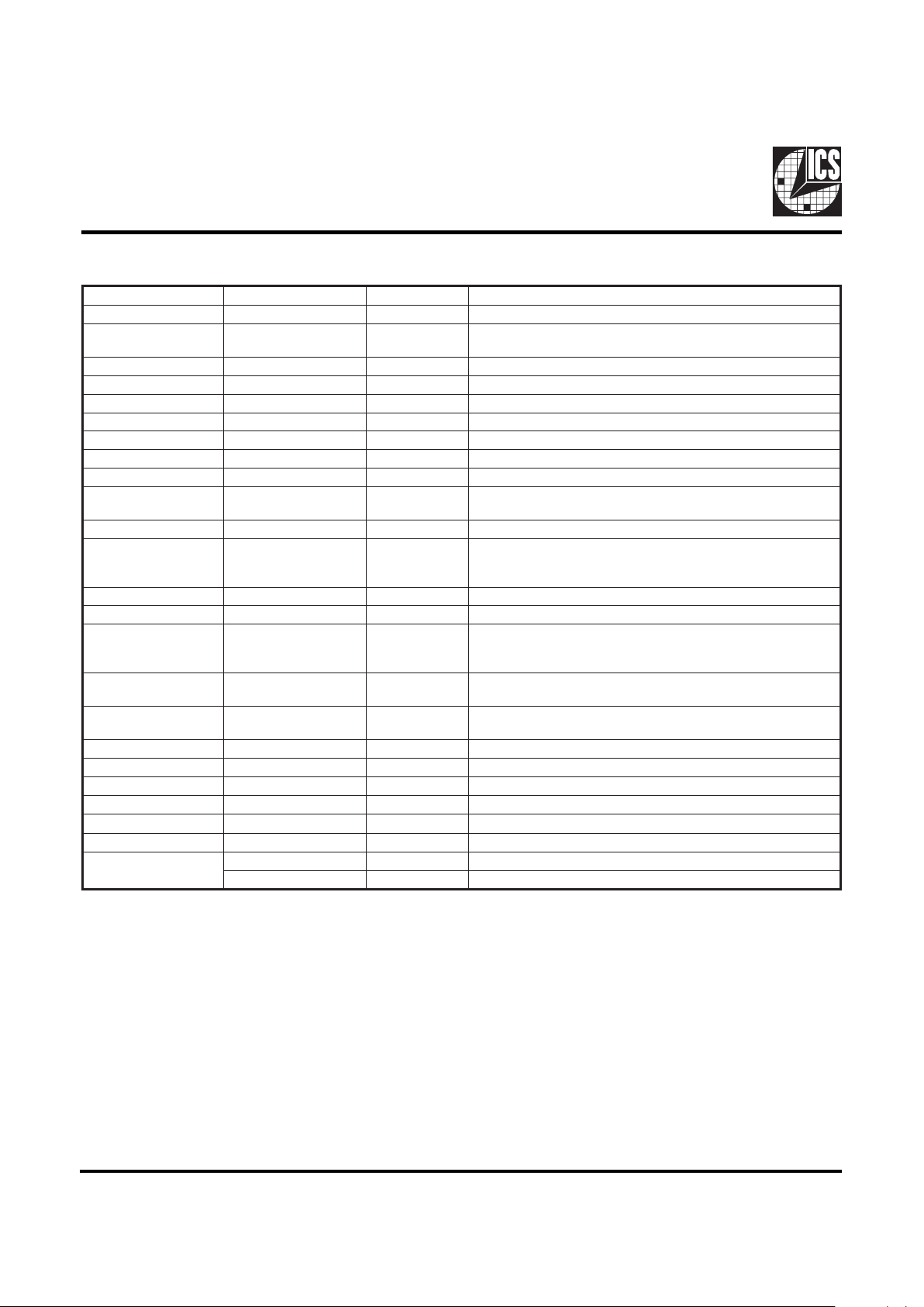
Pin Descriptions
REBMUNNIPEMANNIPEPYTNOITPIRCSED
11DNGRWP.2X,1X,)1:0(FERrofdnuorG
21XNI
Fp33lanretnisah,tupnilatsyrCzHM813.41NI_LATX
2Xmorfrotsiserkcabdeefdnapacdaol
32XTUOFp33pacdaollanretnisah,tuptuolatsyrCTUO_LATX
42DNGRWPstuptuoICProfdnuorG
5F_KLCICPTUO#POTS_ICPybdetceffatoN.tuptuoICPgninnuReerF
01,9,7,6)3:0(KLCICPTUOV3.3elbitapmocLTT.stuptuokcolcICP
82DDVRWPV3.3yllanimon,stuptuoKLCICProfrewoP
113DDVRWPzHM84rofreoP
21zHM84TUOzHM84@tuptuoKLCdexiF
31zHM84_42TUO
,purewopta1=72nipfizHM42;tuptuoKLCdexiF
.purewopta0=72nipfizHM84
413DNGRWPzHM84rofdnuorG
51#6.66/001LESNI
zHM6.66rozHM001gnilbanerofniptceleS
suonorhcnyssyawlaICP(zHM6.66=L,zHM001=H
)zHM3.33
61KLCSNIIroftupnikcolC
2
tupniC
71ATADSNIIroftupniataD
2
tupniC
81#DPNI
selbasid)WOL(evitcanevirdnehwtupnisuonorhcnysA
decalperastuptuollA.ylraeOCVspots,skcolclanretni
.elcyctnerucehtfodneehttaetatsWOLani
91#POTS_UPCNI
spots)WOL(evitcanevirdnehwtupnisuonorhcnysA
.etatsWOLani)1:0(KLCUPC
02#POTS_ICPNI
spots)WOL(evitcanevirdnehwtupnisuonorhcnysA
.detceffatonsiF_KLCICP.etatsWOLani)3:0(KLCICP
12DNGRWPerocehtdna)1:0(KLCUPCrofdnuorG
22DDVRWPerocLLProfrewoP
42,32)0:1(KLCUPCTUOV5.2yllanimonstuptuokcolctsoHdnaUPC
52LDDVRWPV5.2yllanimon,stuptuoUPCrofrewoP
621FERTUOtuptuokcolcecnerefeRzHM813.41
721DDVRWP.stuptuoFERrofrewoP
82
0FERTUOtuptuokcolczHM813.41
#84LESNI.zHM84si31nip,wolnehW.purewoptatupnidehctaL
Page 3
3
ICS9148-46
1. The ICS clock generator is a slave/receiver, I2C component. It can read back the data stored in the latches for verification.
Read-Back will support Intel PIIX4 "Block-Read" protocol.
2. The data transfer rate supported by this clock generator is 100K bits/sec or less (standard mode)
3. The input is operating at 3.3V logic levels.
4. The data byte format is 8 bit bytes.
5. To simplify the clock generator I2C interface, the protocol is set to use only "Block-Writes" from the controller. The
bytes must be accessed in sequential order from lowest to highest byte with the ability to stop after any complete byte
has been transferred. The Command code and Byte count shown above must be sent, but the data is ignored for those
two bytes. The data is loaded until a Stop sequence is issued.
6. At power-on, all registers are set to a default condition, as shown.
General I2C serial interface information
The information in this section assumes familiarity with I2C programming.
For more information, contact ICS for an I2C programming application note.
How to Write:
Controller (host) sends a start bit.
Controller (host) sends the write address D2
(H)
ICS clock will acknowledge
Controller (host) sends a dummy command code
ICS clock will acknowledge
Controller (host) sends a dummy byte count
ICS clock will acknowledge
Controller (host) starts sending first byte (Byte 0)
through byte 5
ICS clock will acknowledge each byte one at a time.
Controller (host) sends a Stop bit
How to Read:
Controller (host) will send start bit.
Controler (host) sends the read address D3
(H)
ICS clock will acknowledge
ICS clock will send the byte count
Controller (host) acknowledges
ICS clock sends first byte (Byte 0) through byte 6
Controller (host) will need to acknowledge each byte
Controller (host) will send a stop bit
Notes:
Controller (Host) ICS (Sl ave/Receiver)
Start Bit
Address
D2
(H)
AC
K
Dummy C ommand Code
AC
K
Dummy Byte Count
ACK
Byte 0
AC
K
Byte 1
AC
K
Byte 2
ACK
Byte 3
AC
K
Byte 4
AC
K
Byte 5
ACK
Byte 6
AC
K
Stop Bit
How to Write:
Controller (Host) ICS (Slave/Receiver)
Start Bit
Address
D3
(H)
AC
K
Byte Coun
t
ACK
Byte
0
ACK
Byte 1
ACK
Byte
2
ACK
Byte
3
ACK
Byte
4
ACK
Byte
5
ACK
Byte
6
ACK
Stop Bit
How to Read:
Page 4

4
ICS9148-46
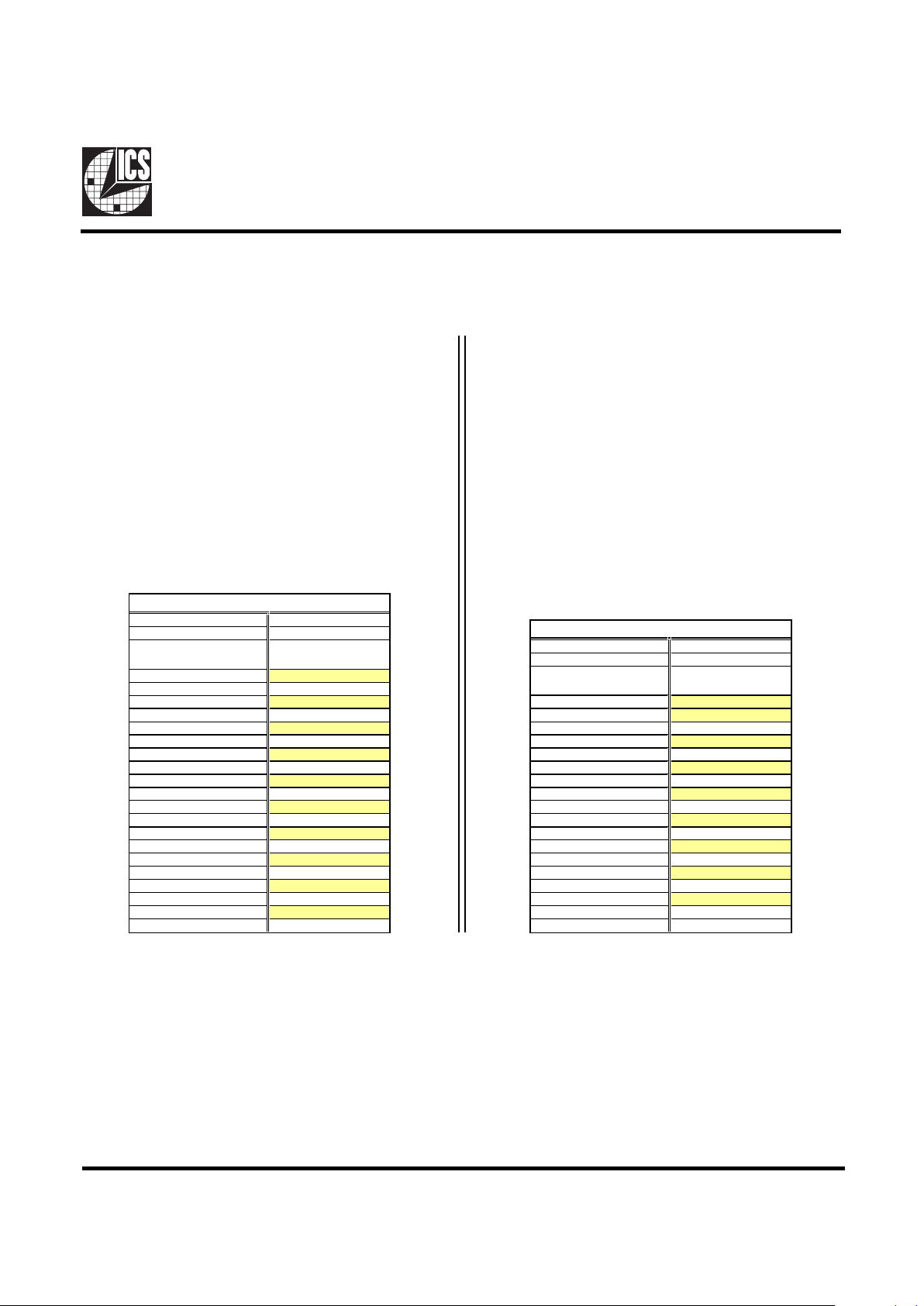
Note: PWD = Power-Up Default
Byte 3: Functionality & Frequency Select
& Spread Slect Register
Notes: 1 = Enabled; 0 = Disabled, outputs held low
Byte 4:
Notes: 1 = Enabled; 0 = Disabled, outputs held low
tiB#niPemaNniPDWP
noitpircseD
0=eulaVtiB1=eulaVtiB
7- - - )devreseR()devreseR(
6- - - )devreseR()devreseR(
5- - - )devreseR()devreseR(
4- - - )devreseR()devreseR(
3- - - )devreseR()devreseR(
2321KLCUPC1
delbasiD
)wol(
delbanE
1- - 0 )devreseR()devreseR(
0420KLCUPC1
)delbasiD(
)wol(
delbanE
Byte 5:
Notes: 1 = Enabled; 0 = Disabled, outputs held low
tiB#niPemaNniPDWP
noitpircseD
0=eulaVtiB1=eulaVtiB
75 F_KLCICP1
delbasiD
)wol(
delbanE
6013KLCICP1
delbasiD
)wol(
delbanE
59 2KLCICP1
delbasiD
)wol(
delbanE
4- - 0 )devreseR()devreseR(
37 1KLCICP1
delbasiD
)wol(
delbanE
26 0KLCICP1
delbasiD
)wol(
delbanE
1- - 0 )devreseR()devreseR(
0- - 0 )devreseR()devreseR(
Byte 6:
Notes: 1 = Enabled; 0 = Disabled, outputs held low
tiB#niPemaNniPDWP
noitpircseD
0=eulaVtiB1=eulaVtiB
7- - 0 )devreseR()devreseR(
6- - 0 )devreseR()devreseR(
5- - 0 )devreseR()devreseR(
4- - 0 )devreseR()devreseR(
3- - 0 )devreseR()devreseR(
2621FER1
)delbasiD(
)wol(
delbanE
1- - 0 )devreseR()devreseR(
0820FER1
)delbasiD(
)wol(
delbanE
Serial Bitmap
tiBnoitpircseDDWP
7
%552.0±daerpSretneC:0
%6.0-ot0daerpSnwoD:1
0
4:6
tiB
456
UPCICP
000
100
010
110
001
101
011
111
5.86
0.57
3.38
6.66
301
211
3.331
001
52.43
5.73
6.14
3.33
3.43
3.73
34.44
33.33
0
3
ybdetcelessiycneuqerF-0
#6.66/001LEStceleserawdrah
evoba4:6ybdetcelessiycneuqerF-1
0
2)devreseR(
01
noitarepolamroN-00
edomtseT-10
NOmurtcerpsdaerpS-01
stuptuollaetatsirT-11
00
Page 5

5
ICS9148-46
Absolute Maximum Ratings
Supply Voltage . . . . . . . . . . . . . . . . . . . . . . . . . . . 7.0 V
Logic Inputs . . . . . . . . . . . . . . . . . . . . . . . . . . . . GND 0.5 V to VDD +0.5 V
Ambient Operating Temperature . . . . . . . . . . . . 0°C to +70°C
Storage Temperature . . . . . . . . . . . . . . . . . . . . . . 65°C to +150°C
Stresses above those listed under Absolute Maximum Ratings may cause permanent damage to the device. These ratings are
stress specifications only and functional operation of the device at these or any other conditions above those listed in the
operational sections of the specifications is not implied. Exposure to absolute maximum rating conditions for extended periods
may affect product reliability.
Electri cal Charact eri sti cs - I nput/ Supply/Com mon O ut put Param et ers
TA = 0 - 70C; Supply Voltage VDD = V
DDL
= 3.3 V +/-5% (unless otherwi se stated)
PARA METER SYMBOL COND ITI ON S MIN TYP MAX U N ITS
Input High Voltage V
IH
2V
DD
+0.3 V
Input Low Voltage V
IL
VSS-0.3 0.8 V
Input High Cur rent I
IH
VIN = V
DD
0.1 5
µ
A
Inpu t L ow Current I
IL1
VIN = 0 V; Inputs with no pull-up resist or s -5 2. 0
µ
A
Inpu t L ow Current I
IL2
VIN = 0 V; Inputs with pull-up resist or s -200 -100
µ
A
Operat ing I
DD3.3OP6 6CL
= 0 pF; Sele c t @ 66M Hz 60 170 m A
Suppl y Current I
DD3.3O P100CL
= 0 pF; Sele ct @ 100MHz 66 170 m A
Power Down I
DD3.3PDCL
= 0 pF; With inp ut add r e s s t o Vdd or GND 3 650
µ
A
Suppl y Current
Input frequency F
i
VDD = 3.3 V; 14.318 MHz
C
IN
Logic Inputs 5 pF
C
INX
X 1 & X2 pins 27 36 45 pF
Transition Time
1
T
trans
To 1s t c rossing of target Freq. 3 ms
Se ttli ng T ime
1
T
s
From 1st crossing to 1% ta rget Freq. 5 ms
Clk S ta bil iz ation
1
T
STAB
From VDD = 3.3 V to 1% target Freq. 3 ms
Skew
1
T
AGP-PCI1VT
= 1.5 V; 1 3. 5 4 ns
1
G uaranteed by des i gn, not 100 % te s ted i n pr odu cti on.
Input Capacitance
1
Electri cal Character ist i cs - I nput/ Supply/ Comm on Out put Param eter s
TA = 0 - 70C; S upply Vol t age VDD = 3.3 V +/-5%, V
DDL
= 2.5 V +/-5% (unless otherwise stated)
PARAMETER SYMBOL CONDITIONS MIN TYP MAX UNITS
Operating I
DD2.5OP66
CL = 0 pF; Select @ 66.8 MHz 16 72 mA
Supply Curr e nt I
DD2.5OP100
CL = 0 pF; Select @ 100 MHz 23 100 mA
Power Down Supply
Current
I
DD2.5PD
CL = 0 pF; With i nput a ddress to
V dd or GND
10 100
µ
A
t
CPU-AGP
00.51ns
t
CPU-PCI2
VT = 1.5 V; VTL = 1.25 V 1 2.6 4 ns
1
Guar a nt e e d by de sign, not 100% tested in produ ct ion.
Skew
1
Page 6

6
ICS9148-46
Electrical Characteri sti cs - CPUCLK
TA = 0 - 70C; VDD = 3.3 V +/-5%, V
DDL
= 2. 5 V +/-5%; CL = 20 pF (unles s otherwise st a ted)
PARA METER SYMBOL COND ITI ON S MIN TYP MAX UNITS
Output High Voltage V
OH2B
IOH = -12.0 m A 2 2.3 V
Output Low Voltage V
OL2B
IOL = 12 mA 0.2 0. 4 V
O utput High Curr e nt I
OH2B
VOH = 1 .7 V -41 -19 mA
Ou tput L ow Curr e nt I
OL2B
VOL = 0.7 V 19 37 mA
Rise Time
t
r2B
1
VOL = 0.4 V, VOH = 2.0 V 1.25 1.6 ns
Fa ll T ime
t
f2B
1
VOH = 2.0 V, VOL = 0 .4 V 1 1.6 ns
Duty Cycle
d
t2B
1
VT = 1.25 V 454855%
Skew
t
sk2B
1
VT = 1.25 V 30 175 ps
Jitter, Cycle -to-cycle
t
jcy
c-cyc2B
1
VT = 1.25 V 15 0 250 ps
Jitter, O ne Sigma
t
j
1s2B
1
VT = 1.25 V 40 150 ps
Jitter, A bsolute
t
jabs2B
1
VT = 1.25 V -2 50 140 + 250 ps
1
G uaranteed by de s i gn, not 100% tes te d in production.
Electri cal Character ist ics - PCICLK
TA = 0 - 70C; VDD = V
DDL
= 3.3 V +/-5%; CL = 30 pF
PARAMETER SYMBOL CONDITIONS MIN TYP MAX UNITS
O utput High Voltage V
OH1
IOH = -11 mA 2.4 3.1 V
Output Low Voltage V
OL1
IOL = 9.4 mA 0.1 0.4 V
Ou tput High Current I
OH1
VOH = 2.0 V -62 -22 mA
Output Low Current I
OL1
VOL = 0.8 V 16 57 mA
Rise Time
1
t
r1
VOL = 0.4 V, VOH = 2.4 V 1.5 2 ns
Fall Time
1
t
f1
VOH = 2.4 V , VOL = 0.4 V 1.1 2 ns
Duty Cycle
1
d
t1
VT = 1.5 V 45 50 55 %
Skew
1
t
sk1
VT = 1.5 V 140 500 ps
Jitter, One Sigm a
1
t
j1s1
VT = 1.5 V 17 150 ps
Jitter, Absol ute
1
t
jabs1
VT = 1.5 V -500 70 500 ps
1
Guar a nte e d by design, not 100% tested i n productio n.
Page 7

7
ICS9148-46
Electri cal Characteri sti cs - REF
TA = 0 - 70C; VDD = V
DDL
= 3.3 V +/-5%; CL = 20 pF (unless otherwise stated)
PARAMETER SYMBOL CONDITIONS MIN TYP MAX UNITS
O utput High Voltage V
OH5
IOH = -12 mA 2.6 3.1 V
Output Low Voltage V
OL5
IOL = 9 mA 0.17 0.4 V
Ou tput Hi gh Current I
OH5
VOH = 2.0 V -44 -22 m A
Output Low Current I
OL5
VOL = 0.8 V 29 42 mA
Rise Time
1
t
r5
VOL = 0.4 V, VOH = 2.4 V 1.4 2 ns
Fall Time
1
t
f5
VOH = 2.4 V , VOL = 0.4 V 1.1 2 ns
Duty Cycle
1
d
t5
VT = 1.5 V 47 54 57 %
Jitter, O ne S igm a
1
t
j1s5
VT = 1.5 V 1 3 %
Jitter, Absol ute
1
t
jabs5
VT = 1.5 V 3 5 %
1
Guar a nteed by design, not 100% tested in producti o n.
Electri cal Characteri sti cs - 48, 24 MHz
TA = 0 - 70C; VDD = V
DDL
= 3.3 V +/-5%; CL = 20 pF (unless otherwise stated)
PARAMETER SYMBOL CONDITIONS MIN TYP MAX UNITS
O utput High Voltage V
OH5
IOH = -12 m A 2.6 3 V
Output Low Voltage V
OL5
IOL = 9 mA 0.14 0.4 V
Ou tput Hi gh Current I
OH5
VOH = 2.0 V -44 -22 m A
Output Low Current I
OL5
VOL = 0.8 V 16 42 mA
Rise Time
1
t
r5
VOL = 0.4 V, VOH = 2.4 V 1.2 4 ns
Fall Time
1
t
f5
VOH = 2.4 V , VOL = 0.4 V 1.2 4 ns
Duty Cycle
1
d
t5
VT = 1.5 V 45 52 55 %
Jitter, O ne S igm a
1
t
j1s5
VT = 1.5 V 1 3 %
Jitter, Absol ute
1
t
jabs5
VT = 1.5 V 3 5 %
1
Guar a nteed by design, not 100% tested in producti o n.
Page 8

8
ICS9148-46
General Layout Precautions:
1) Use a ground plane on the top layer
of the PCB in all areas not used by
traces.
2) Make all power traces and vias as
wide as possible to lower inductance.
Notes:
1 All clock outputs should have series
terminating resistor. Not shown in all
places to improve readibility of
diagram
2 Optional EMI capacitor should be
used on all CPU, SDRAM, and PCI
outputs.
3 Optional crystal load capacitors are
recommended.
Capacitor Values:
C1, C2 : Crystal load values determined by user
All unmarked capacitors are 0.01µF ceramic
Page 9
9
ICS9148-46
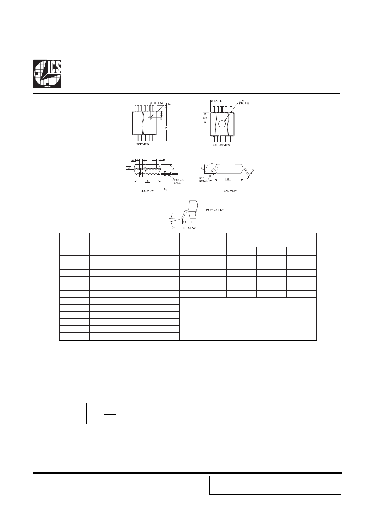
28 Pin SSOP Package
LOBMYS
NOMMOC
SNOISNEMID
SNOITAIRAV
D
.NIM.MON.XAMN .NIM.MON.XAM
A860.0370.0870.041932.0442.0942.0
1A200.0500.0800.061932.0442.0942.0
2A660.0860.0070.002872.0482.0982.0
b010.0210.0510.042813.0323.0823.0
c400.0600.0800.082793.0204.0704.0
DsnoitairaVeeS03793.0204.0704.0
E502.0902.0212.0
eCSB6520.0
H103.0703.0113.0
L520.0030.0730.0
NsnoitairaVeeS
∝
°0°4°8
ICS reserves the right to make changes in the device data identified in
this publication without further notice. ICS advises its customers to
obtain the latest version of all device data to verify that any
information being relied upon by the customer is current and accurate.
Ordering Information
ICS9148yF-46
Pattern Number (2 or 3 digit number for parts with ROM code patterns)
Package Type
F=SSOP
Revision Designator (will not correlate with datasheet revision)
Device Type (consists of 3 or 4 digit numbers)
Prefix
ICS, AV = Standard Device
Example:
ICS XXXX y F - PPP
 Loading...