

Page 1
Integrated
Circuit
Systems, Inc.
General Description Features
ICS9148-37
ICS reserves the right to make changes in the device data identified in this
publication without further notice. ICS advises its customers to obtain the latest
version of all device data to verify that any information being relied upon by the
customer is current and accurate.
Block Diagram
Pentium is a trademark of Intel Corporation
I2C is a trademark of Philips Corporation
Frequency Generator & Integrated Buffers for PENTIUM/Pro
TM
9148-37 Rev F 4/25/99
Pin Configuration
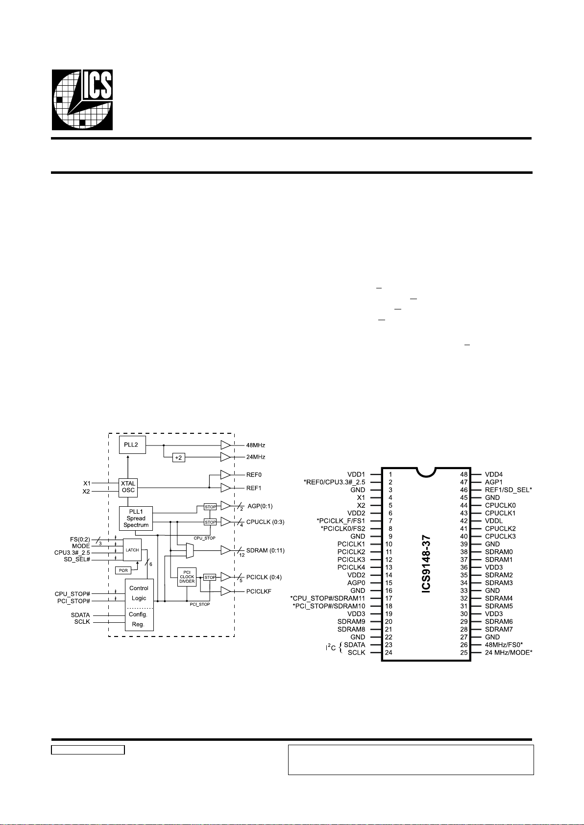
Generates the following system clocks:
- 4 CPU(2.5V/3.3V) upto 100MHz.
- 6 PCI(3.3V) @ 33.3MHz
- 2AGP(3.3V) @ 2 x PCI
- 12 SDRAMs(3.3V) @ either CPU or AGP
- 2 REF (3.3V) @ 14.318MHz
Skew characteristics:
- CPU CPU
<250ps
- SDRAM SDRAM
< 250ps
- CPU SDRAM
< 250ps
- CPUAGP: < 1ns
- CPU(early) PCI : 1-4ns
Supports Spread Spectrum modulation +0.25, ±0.6%
Serial I2C interface for Power Management, Frequency
Select, Spread Spectrum.
Efficient Power management scheme through PCI and CPU
STOP CLOCKS.
Uses external 14.318MHz crystal
48 pin 300mil SSOP.
48-Pin SSOP
Power Groups
VDD1 = REF (0:1), X1, X2
VDD2 = PCICLK_F, PCICLK(0:5)
VDD3 = SDRAM (0:11), supply for PLL core,
24 MHz, 48MHz
VDD4 = AGP (0:1)
VDDL = CPUCLK (0:3)
* Internal Pull-up Resistor of
240K to 3.3V on indicated inputs
The ICS9148-37 is the single chip clock solution for Desktop/
Notebook designs using the VIA MVP3 style chipset. It
provides all necessary clock signals for such a system.
Spread spectrum may be enabled through I2C programming.
Spread spectrum typically reduces system EMI by 8dB to
10dB. This simplifies EMI qualification without resorting to
board design iterations or costly shielding. The ICS9148-37
employs a proprietary closed loop design, which tightly
controls the percentage of spreading over process and
temperature variations.
Serial programming I2C interface allows changing functions,
stop clock programming and frequency selection. The SD_SEL
latched input allows the SDRAM frequency to follow the
CPUCLK frequency(SD_SEL=1) or the AGP clock
frequency(SD_SEL=0)
Page 2
2
ICS9148-37
Pin Descriptions
Notes:
1: Internal Pull-up Resistor of 240K to 3.3V on indicated inputs
2: Bidirectional input/output pins, input logic levels are latched at internal power-on-reset. Use 10Kohm resistor to
program logic Hi to VDD or GND for logic low.
REBMUNNIPEMANNIPEPYTNOITPIRCSED
11DDVRWPV3.3lanimon,ylppusrewopLATX,)2:0(feR
2
0FERTUO.kcolcecnereferzHM813.41
5.2_#3.3UPC
2,1
NI
V3.3=WOL,UPCV5.2=hgiH.V5.2roV3.3si2LDDVrehtehwsetacidnI
UPC
1
tupnidehctaL.
2
,72,22,61,9,3
54,93,33
DNGRWPdnuorG
41XNI
kcabdeefdna)Fp33(pacdaollanretnisah,tupnilatsyrC
2Xmorfrotsiser
52XTUO
daollanretnisaH.zHM813.41yllanimon,tuptuolatsyrC
)Fp33(pac
41,62DDVRWPV3.3lanimon,)5:0(KLCICPdnaF_KLCICProfylppuS
7
F_KLCICPTUO
wekssn4-1htiwsKLCUPChtiwsuonorhcnyS.tuptuokcolcICPgninnureerF
#POTS_ICPybdetceffatonsisihT)ylraeUPC(
1SF
2,1
NI
ehtsenimretedsnipSFrehtohtiwgnolA.tupnIdehctaL.niptcelesycneuqerF
.seicneuqerfPGA&ICP,MARDS,UPC
8
0KLCICPTUO )ylraeUPC(wekssn4-1htiwsKLCUPCsuonorhcnyS.tuptuokcolcICP
2SF
2,1
NI
ehtsenimretedsnipSFrehtohtiwgnolAtupnIdehctaL.niptcelesycneuqerF
.seicneuqerfPGA&ICP,MARDS,UPC
31,21,11,01)4:1(KLCICPTUO )ylraeUPC(wekssn4-1htiwsKLCUPCsuonorhcnyS.stuptuokcolcICP
74,51)1:0(PGATUO.4DDVybderewop,stuptuotroPcihparGdecnavdA
71
#POTS_UPC
1
NI
0cigoltaskcolc)1:0(PGAdna)3:0(KLCUPCstlahtupnisuonorhcnysasihT
)0=EDOM,edoMeliboMni(woltupninehw,level
11MARDSTUO
.tupnidehctalLES_DSehtybdetcelessiycneuqerF.tuptuokcolcMARDS
ycneuqerfUPC=ycneuqerfMARDSsesuacnorewopta1=LES_DS
ycneuqerfPGA=ycneuqerfMARDSsesuacnorewopta0=LES_DS
81
#POTS_ICP
1
NI
nehw,level0cigoltaskcolc)5:0(KLCICPstlahtupnisuonorhcnysasihT
)0=EDOM,edomelibomnI(woltupni
01MARDSTUO
.tupnidehctalLES_DSehtybdetcelessiycneuqerF.tuptuokcolcMARDS
ycneuqnerfUPC=ycneuqerfMARDSsesuacnorewopta1=LES_DS
ycneuqerfPGA=ycneuqerfMARDSsesuacnorewopta0=LES_DS
,13,92,82,12,02
83,73,53,43,23
)9:0(MARDSTUO
.tupnidehctalLES_DSehtybdetcelessiycneuqerF.stuptuokcolcMARDS
ycneuqerfUPC=ycneuqerfMARDSsesuacnorewopta1=LES_DS
ycneuqerfPGA=seicneuqerfMARDSsesuacnorewopta0=LES_DS
63,03,913DDVRWP
,skcolczHM84,42dnaeroCUPC,)11:0(MARDSrofylppuS
.V3.3lanimon
32ATADSNIIroftupniataD
2
.tupnilairesC
42KLCSNIIfotupnikcolC
2
tupniC
52
zHM42TUO.gnimitO/IrepuSrof,kcolctuptuozHM42
EDOM
2,1
NI
.edoMeliboM=0,edoMpotkseD=1,niptcelesnoitcnuf81nip,71niP
.tupnIdehctaL
62
zHM84TUO.gnimitBSUrof,kcolctuptuozHM84
0SF
2,1
NI
ehtsenimretedsnipSFrehtohtiwgnolAtupnIdehctaL.niptcelesycneuqerF
.seicneuqerfPGA&ICP,MARDS,UPC
44,34,14,04)3:0(KLCUPCTUOwoL=#POTS_UPCfiwoL.2LDDVybderewop,stuptuokcolcUPC
24LDDVRWPlanimonV3.3roV5.2rehtie,)3:0(UPCrofylppuS
64
1FERTUO.kcolcecnereferzHM813.41
LES_DSNI
PGAro)1=LESDS(UPCrehtiestcelesnOrewoPtatupnidehctaL
.stuptuokcolcMARDSehtrofseicneuqerf)0=LES_DS(
844DDVRWP)1:0(PGArofylppuS
Page 3
3
ICS9148-37
Functionality
VDD1, 2, 3, 4 = 3.3V±5%, V
DDL
= 2.5V ±5% or 3.3 ±5%, TA= 0 to 70°C
Crystal (X1, X2) = 14.31818MHz
5.2_#3.3UPC
leveltupnI
)ataDdehctaL(
rofdetceleSreffuB
:tanoitarepo
1DDVV5.2
0DDVV3.3
CPU 3.3#_2.5V Buffer selector for CPUCLK drivers.
Power Management Functionality
Mode Pin - Power Management Input Control
52niP,EDOM
)tupnIdehctaL(
71niP81niP
0
#POTS_UPC
)TUPNI(
#POTS_ICP
)TUPNI(
1
11MARDS
)TUPTUO(
01MARDS
)TUPTUO(
#POTS_UPC#POTS_ICP
,PGA
KLCUPC
stuptuO
KLCICP
)5:0(
,F_KLCICP
,FER
zHM84/42
MARDSdna
latsyrC
CSO
OCV
01 woLdeppotSgninnuRgninnuRgninnuRgninnuR
11 gninnuRgninnuRgninnuRgninnuRgninnuR
10 gninnuRwoLdeppotSgninnuRgninnuRgninnuR
2SF1SF0SF
UPC
)zHM(
)zHM(MARDS
)zHM(ICP)zHM(PGA
1=LES_DS0=LES_DS
111 0010016.663.336.66
110 52.5952.595.3657.135.36
101 3.383.386.663.336.66
100 5757060306
011 5757575.7357
010 5.865.865.8652.435.86
001 8.668.668.664.338.66
000 0606060306
Page 4
4
ICS9148-37
1. The ICS clock generator is a slave/receiver, I2C component. It can read back the data stored in the latches for verification.
Read-Back will support Intel PIIX4 "Block-Read" protocol.
2. The data transfer rate supported by this clock generator is 100K bits/sec or less (standard mode)
3. The input is operating at 3.3V logic levels.
4. The data byte format is 8 bit bytes.
5. To simplify the clock generator I2C interface, the protocol is set to use only "Block-Writes" from the controller. The
bytes must be accessed in sequential order from lowest to highest byte with the ability to stop after any complete byte
has been transferred. The Command code and Byte count shown above must be sent, but the data is ignored for those
two bytes. The data is loaded until a Stop sequence is issued.
6. At power-on, all registers are set to a default condition, as shown.
General I2C serial interface information
The information in this section assumes familiarity with I2C programming.
For more information, contact ICS for an I2C programming application note.
How to Write:
Controller (host) sends a start bit.
Controller (host) sends the write address D2
(H)
ICS clock will acknowledge
Controller (host) sends a dummy command code
ICS clock will acknowledge
Controller (host) sends a dummy byte count
ICS clock will acknowledge
Controller (host) starts sending first byte (Byte 0)
through byte 5
ICS clock will acknowledge each byte one at a time.
Controller (host) sends a Stop bit
How to Read:
Controller (host) will send start bit.
Controler (host) sends the read address D3
(H)
ICS clock will acknowledge
ICS clock will send the byte count
Controller (host) acknowledges
ICS clock sends first byte (Byte 0) through byte 5
Controller (host) will need to acknowledge each byte
Controller (host) will send a stop bit
Notes:
Controller (Host) ICS (Slave/Receiver)
Start Bit
Address
D3
(H)
AC
K
Byte Count
ACK
Byte
0
ACK
Byte 1
ACK
Byte
2
ACK
Byte
3
ACK
Byte 4
ACK
Byte
5
ACK
Stop Bit
How to Read:
Controller (Host) ICS (Slave/Receiver)
Start Bit
Address
D2
(H)
AC
K
Dummy Command Code
AC
K
Dummy Byte Count
AC
K
Byte 0
AC
K
Byte 1
AC
K
Byte 2
ACK
Byte 3
AC
K
Byte 4
AC
K
Byte 5
AC
K
Stop Bit
How to Write:
Page 5
5
ICS9148-37
Byte 1: CPU, Active/Inactive Register
(1 = enable, 0 = disable)
Byte 2: PCI Active/Inactive Register
(1 = enable, 0 = disable)
Notes:
1. Inactive means outputs are held LOW and are disabled
from switching.
Notes:
1. Inactive means outputs are held LOW and are disabled
from switching.
tiB#niPDWPnoitpircseD
7tiB-1 )devreseR(
6tiB-1 )devreseR(
5tiB-1 )devreseR(
4tiB-1 )devreseR(
3tiB041 )tcanI/tcA(3KLCUPC
2tiB141 )tcanI/tcA(2KLCUPC
1tiB341 )tcanI/tcA(1KLCUPC
0tiB441 )tcanI/tcA(0KLCUPC
tiB#niPDWPnoitpircseD
7tiB-1 )devreseR(
6tiB71 )tcanI/tcA(F_KLCICP
5tiB511 )tcanI/tcA(0PGA
4tiB311 )tcanI/tcA(4KLCICP
3tiB211 )tcanI/tcA(3KLCICP
2tiB111 )tcanI/tcA(2KLCICP
1tiB011 )tcanI/tcA(1KLCICP
0tiB81 )tcanI/tcA(0KLCICP
Byte0: Functionality and Frequency Select Register
(default = 0)
Serial Configuration Command Bitmap
tiBnoitpircseDDWP
7tiB
noitaludoMmurtcepSdaerpS%52.0±-0
noitaludoMmurtcepSdaerpS%6.0±-1
0
tiB
4:6
5tiB6tiB
4tiB
111
011
101
001
110
010
100
000
kcolCUPC
001
52.59
3.38
57
57
5.86
8.66
06
ICP
3.33
57.13
3.33
03
5.73
52.43
4.33
03
PGA
6.66
5.36
6.66
06
57
5.86
8.66
06
etoN
1
3tiB
,tceleserawdrahybdetcelessiycneuqerF-0
stupnIdehctaL
)evoba(4:6tiBybdetcelessiycneuqerF-1
0
.epytdaerpsretnecmurtcepSdaerpS-0
.epytdaerpsnwodmurtcepSdaerpS-1
0
1tiB
lamroN-0
delbanEmurtcepSdaerpS-1
0
0tiB
gninnuR-0
stuptuollaetatsirT-1
0
Page 6

6
ICS9148-37
Byte 3: SDRAM Active/Inactive Register
(1 = enable, 0 = disable)
Notes:
1. Inactive means outputs are held LOW and are disabled
from switching.
tiB#niPDWPnoitpircseD
7tiB821 )tcanI/tcA(7MARDS
6tiB921 )tcanI/tcA(6MARDS
5tiB131 )tcanI/tcA(5MARDS
4tiB231 )tcanI/tcA(4MARDS
3tiB431 )tcanI/tcA(3MARDS
2tiB531 )tcanI/tcA(2MARDS
1tiB731 )tcanI/tcA(1MARDS
0tiB831 )tcanI/tcA(0MARDS
Byte 4: SDRAM Active/Inactive Register
(1 = enable, 0 = disable)
Byte 5: Peripheral Active/Inactive Register
(1 = enable, 0 = disable)
Notes:
1. Inactive means outputs are held LOW and are disabled
from switching.
Notes:
1. Inactive means outputs are held LOW and are disabled
from switching.
tiB#niPDWPnoitpircseD
7tiB-1 )devreseR(
6tiB-1 )devreseR(
5tiB-1 )devreseR(
4tiB-1 )devreseR(
3tiB711
)tcanI/tcA(11MARDS
)ylnOedoMpotkseD(
2tiB811
)tcanI/tcA(01MARDS
)ylnOedoMpotkseD(
1tiB021 )tcanI/tcA(9MARDS
0tiB121 )tcanI/tcA(8MARDS
tiB#niPDWPnoitpircseD
7tiB-1 )devreseR(
6tiB-1 )devreseR(
5tiB-1 )devreseR(
4tiB741 )tcanI/tcA(1PGA
3tiB-1 )devreseR(
2tiB-1 )devreseR(
1tiB641 )tcanI/tcA(1FER
0tiB21 )tcanI/tcA(0FER
Page 7

7
ICS9148-37
CPU_STOP# Timing Diagram
CPU_STOP# is an asychronous input to the clock synthesizer. It is used to turn off the CPU clocks for low power operation.
CPU_STOP# is synchronized by the ICS9148-37. The minimum that the CPU clock is enabled (CPU_STOP# high pulse) is 100
CPU clocks. All other clocks will continue to run while the CPU clocks are disabled. The CPU clocks will always be stopped in
a low state and start in such a manner that guarantees the high pulse width is a full pulse. CPU clock on latency is less than 4
CPU clocks and CPU clock off latency is less than 4 CPU clocks.
Notes:
1. All timing is referenced to the internal CPU clock.
2. CPU_STOP# is an asynchronous input and metastable conditions may exist. This signal is synchronized
to the CPU clocks inside the ICS9148-37.
3. All other clocks continue to run undisturbed. (including SDRAM outputs).
Page 8

8
ICS9148-37
PCI_STOP# Timing Diagram
PCI_STOP# is an asynchronous input to the ICS9148-37. It is used to turn off the PCICLK (0:5) clocks for low power operation.
PCI_STOP# is synchronized by the ICS9148-37 internally. The minimum that the PCICLK (0:5) clocks are enabled (PCI_STOP#
high pulse) is at least 10 PCICLK (0:5) clocks. PCICLK (0:5) clocks are stopped in a low state and started with a full high pulse
width guaranteed. PCICLK (0:5) clock on latency cycles are only one rising PCICLK clock off latency is one PCICLK clock.
Notes:
1. All timing is referenced to the Internal CPUCLK (defined as inside the ICS9148 device.)
2. PCI_STOP# is an asynchronous input, and metastable conditions may exist. This signal is required to be synchronized
inside the ICS9148.
3. All other clocks continue to run undisturbed.
4. CPU_STOP# is shown in a high (true) state.
Page 9

9
ICS9148-37
Pins 2, 7, 8, 25, 26 and 46 on the ICS9148-37 serve as dual
signal functions to the device. During initial power-up, they
act as input pins. The logic level (voltage) that is present on
these pins at this time is read and stored into a 4-bit internal
data latch. At the end of Power-On reset, (see AC
characteristics for timing values), the device changes the
mode of operations for these pins to an output function. In
this mode the pins produce the specified buffered clocks to
external loads.
To program (load) the internal configuration register for these
pins, a resistor is connected to either the VDD (logic 1)
power supply or the GND (logic 0) voltage potential. A 10
Kilohm(10K) resistor is used to provide both the solid CMOS
programming voltage needed during the power-up
programming period and to provide an insignificant load on
the output clock during the subsequent operating period.
Figs. 1 and 2 show the recommended means of implementing
this function. In Fig. 1 either one of the resistors is loaded
onto the board (selective stuffing) to configure the devices
internal logic. Figs. 2a and b provide a single resistor loading
option where either solder spot tabs or a physical jumper
header may be used.
Shared Pin Operation Input/Output Pins
Fig. 1
These figures illustrate the optimal PCB physical layout
options. These configuration resistors are of such a large
ohmic value that they do not effect the low impedance clock
signals. The layouts have been optimized to provide as little
impedance transition to the clock signal as possible, as it
passes through the programming resistor pad(s).
Page 10

10
ICS9148-37
Fig. 2a
Fig. 2b
Page 11

11
ICS9148-37
Absolute Maximum Ratings
Supply Voltage. . . . . . . . . . . . . . . . . . . . . . . . . . . 7.0 V
Logic Inputs . . . . . . . . . . . . . . . . . . . . . . . . . . . . GND 0.5 V to VDD +0.5 V
Ambient Operating Temperature . . . . . . . . . . . . 0°C to +70°C
Storage Temperature . . . . . . . . . . . . . . . . . . . . . . 65°C to +150°C
Case Temperature . . . . . . . . . . . . . . . . . . . . . . . . 115°C
Stresses above those listed under Absolute Maximum Ratings may cause permanent damage to the device. These ratings are
stress specifications only and functional operation of the device at these or any other conditions above those listed in the
operational sections of the specifications is not implied. Exposure to absolute maximum rating conditions for extended periods
may affect product reliability.
Electrical Characte ristics - Input/Supply/Common Output Par am eters
TA = 0 - 70C; Supp ly Voltage VDD = 3.3 V +/-5%, V
DDL
= 2.5 V +/ -5% (unle s s otherwise st a te d)
PARAMETER SYMBOL CONDITIONS MIN TYP MAX UNITS
Operating I
DD2.5OP
CL = 0 pF; 66.8 MHz 10 20 mA
Suppl y Cu rrent
T
CPU-SDRAM2VT
= 1.5 V; VTL = 1 .25 V; SDRAM Leads -500 200 500 ps
T
CPU-PCI2VT
= 1.5 V; VTL = 1.25 V; CPU Leads
12.74 ns
1
G ua ranteed by d e sign, not 100% t e sted in pr odu c t i on.
Skew
1
Electrical Characte ristics - Input/Supply/Common Output Par am eters
TA = 0 - 70C; Supp ly Voltage VDD = V
DDL
= 3 .3 V +/-5% (unless ot h e rwise stat e d)
PARAMETER SYMBOL CONDITIONS MIN TYP MAX UNITS
Inpu t High Volt age V
IH
2V
DD
+0.3 V
In put Low Voltage V
IL
VSS-0.3 0.8 V
Input High Current I
IH
VIN = V
DD
0.15mA
Input Low Current I
IL1
VIN = 0 V; Input s with no pull -up resistor s - 5 2.0 mA
Input Low Current I
IL2
VIN = 0 V; Input s with pul l-up re sistor s -200 - 100 mA
Operating I
DD3.3OP
CL = 0 pF; 66.8 MHz 100 160 mA
Suppl y Cu rrent
In put freque ncy F
i
VDD = 3.3 V; 14.318 MHz
Input Ca pa c it a nce
1
C
IN
Logic Inputs 5 pF
C
INX
X 1 & X2 pins 27 36 45 pF
Transition Time
1
T
trans
To 1st cros sing of ta rget Freq. 2 ms
Settling Time
1
T
s
From 1st cr ossing to 1% ta rget F req. ms
Clk Stabilization
1
T
STAB
From VDD = 3.3 V to 1% target Freq. 2 ms
T
CPU-SDRAM1VT
= 1 .5 V; SDRAM Leads -50 0 200 500 ps
T
CPU-PCI1VT
= 1.5 V; CPU Leads 1 2.8 4 ns
T
CPU-AGPVT
= 1.5 V; CPU Leads
-1 0 1 ns
1
G ua ranteed by d e sign, not 100% t e sted in pr odu c t i on.
Skew
1
Page 12

12
ICS9148-37
Ele ctri cal Characteristics - CP U
TA = 0 - 70C; VDD = V
DDL
= 3.3 V +/ -5%; CL = 10 - 20 pF (unless otherwis e stated)
PARAMETER SYMBOL CONDITIONS MIN TYP MAX UNITS
Output High Voltage V
OH2AIOH
= -28 mA 2.5 2.6 V
Output Low Voltage V
OL2AIOL
= 27 m A 0.35 0.4 V
O utpu t High Cur rent I
OH2A
VOH = 2.0 V -29 -23 mA
O utput Low Current I
OL2A
VOL = 0.8 V 33 37 mA
Rise Time t
r2A
1
VOL = 0.4 V, VOH = 2.4 V 1.75 2 ns
Fall Time t
f2A
1
VOH = 2.4 V, VOL = 0.4 V 1.1 2 ns
Duty Cycle d
t2A
1
VT = 1.5 V 45 50 55 %
Skew t
sk2A
1
VT = 1.5 V 50 250 ps
Jitter, One Sigma t
j1s2A
1
VT = 1.5 V 65 150 ps
Jitter, Abs olute
t
jabs2A
1
VT = 1.5 V
-250 165 250 ps
1
G ua ranteed by de sign, not 100% tested i n production.
Ele ct rical C haracter istics - CPU
TA = 0 - 70C; VDD = 3.3 V +/-5%, V
DDL
= 2.5 V +/-5%; CL = 10 - 20 pF (unless other wise state d)
PARAMETER SYMBOL CONDITIONS MIN TYP MAX UNITS
Ou tput High Volta ge VOH2B I
OH
= -8 mA 2 2.2 V
Output Low Voltage VOL2B I
OL
= 12 mA 0.3 0.4 V
Output High Current IOH2B V
OH
= 1.7 V -20 -16 mA
O utput Low Current IOL2B V
OL
= 0.7 V 19 26 mA
Rise Time
tr2B
1
VOL = 0.4 V, VOH = 2.0 V 1.5 1.8 ns
Fa ll T ime
tf2B
1
VOH = 2.0 V, VOL = 0.4 V 1.6 1.8 ns
Duty Cycle
dt2B
1
VT = 1.25 V 404755%
Skew
tsk2B
1
VT = 1.25 V 60 250 ps
Jitter, Single Edge
Displacement
2
tjsed2B
1
VT = 1.25 V 200 250 ps
Jitter, One S igma
tj1s2B
1
VT = 1.25 V 65 150 ps
Jitter, Abs olute
tjabs2B
1
VT = 1.25 V -300 160 300 ps
1
G ua ranteed by de sign, not 100% t ested in production.
2
Edge displac e ment of a per iod relative to a 10-clock-cycle rolling aver a ge period.
Page 13

13
ICS9148-37
Ele ctric al Characteristics - P CI
TA = 0 - 70C; VDD = V
DDL
= 3.3 V +/ -5%; CL = 30 pF (unless otherwise st a t e d)
PARAMETER SYMBOL CONDITIONS MIN TYP MAX UNITS
Ou tput High V olt age V
OH1IOH
= -28 mA 2.4 3 V
Output Low Voltage V
OL1IOL
= 23 mA 0.2 0.4 V
O utp ut High Cur rent I
OH1
VOH = 2 .0 V -60 -40 mA
Output Low Current I
OL1
VOL = 0.8 V 41 50 mA
Rise Time t
r1
1
VOL = 0.4 V, VOH = 2.4 V 1.8 2 ns
Fall Time t
f1
1
VOH = 2.4 V, VOL = 0.4 V 1.6 2 ns
Duty Cycle d
t1
1
VT = 1.5 V 45 51 55 %
Skew t
sk1
1
VT = 1.5 V 130 250 ps
Jitter, One Si gma
1
t
j1s1a
VT = 1.5 V, synchr onous 4 0 1 50 ps
t
j1s1b
VT = 1.5 V, asynchronous 200 250 ps
Jitter, Absolute
1
tab
s1aVT
= 1.5 V, synchr onous - 250 1 35 250 ps
t
jabs1bVT
= 1.5 V, asynchronous
-650 500 650 ps
1
G ua ranteed by de sign, not 100% t est ed in production.
Ele ctri c al Characteri stics - SDRAM
TA = 0 - 70C; VDD = V
DDL
= 3.3 V +/-5%; CL = 30 p F
PARAMETER SYMBOL CONDITIONS MIN TYP MAX UNITS
O utput High Volt a ge V
OH1IOH
= -28 mA 2.4 3 V
Output Low Voltage V
OL1IOL
= 23 mA 0.2 0.4 V
Ou tput High Cur rent I
OH1
VOH = 2 .0 V -60 -40 mA
Output Low Current I
OL1
VOL = 0.8 V 41 50 m A
Rise Time
1
T
r1
VOL = 0.4 V, VOH = 2.4 V 1. 75 2 ns
Fall T im e
1
T
f1
VOH = 2.4 V, VOL = 0.4 V 1.5 2 ns
Duty Cycle
1
D
t1
VT = 1.5 V 45 50 55 %
Skew
1
T
sk1
VT = 1.5 V 200 500 ps
Jitter, One Sigma
1
T
j1s1
VT = 1.5 V 50 150 ps
Jitter, Abs olute
1
T
jabs1
VT = 1.5 V (with s yn c hronous PCI) -250 +250 ps
Jitter, Abs olute
1
T
jabs1
VT = 1.5 V (with asynchronous PCI )
-400 400 ps
1
G ua ranteed by d e sign, not 100% t e sted in pr odu c t i on.
Page 14

14
ICS9148-37
Ele ctri cal Characteristics - A GP
TA = 0 - 70C; VDD = V
DDL
= 3.3 V +/-5%; CL = 30 pF (unless otherwise s ta t ed)
PARAMETER SYMBOL CONDITIONS MIN TYP MAX UNITS
Output High Voltage V
OH1IOH
= -28 mA 2.4 3 V
O ut put Low V o l ta ge V
OL1IOL
= 23 mA 0.2 0.4 V
Ou tput High Current I
OH1
VOH = 2.0 V -60 -40 mA
Output Low Current I
OL1
VOL = 0.8 V 41 50 mA
Rise Time t
r1
1
VOL = 0.4 V, VOH = 2.4 V 1.1 2 ns
Fall Time t
f1
1
VOH = 2.4 V, VOL = 0.4 V 1 2 ns
Duty Cycle d
t1
1
VT = 1.4 V 45 49 55 %
Skew t
sk1
1
VT = 1.5 V 130 250 ps
Jitter , One Sigma
1
t
j1s1
VT = 1.5 V 2 3 %
Jitter, Absolute
1
t
abs1a
VT = 1.5 V, s ync hronous -5 2.5 5 %
t
jabs1b
VT = 1.5 V, asynchronous
-6 4.5 6 %
1
G uar a nt eed by de sign, not 100% tested in pro duction.
Ele ctric al Characteri stics - 24MHz, 48MHz, RE F0
TA = 0 - 70C; VDD = V
DDL
= 3.3 V +/-5%; CL = 10 -20 pF (unless o t he rwise state d)
PARAMETER SYMBOL CONDITIONS MIN TYP MAX UNITS
Ou tput High V olt a g e V
OH5IOH
= -16 mA 2.4 2.6 V
Output Low Voltage V
OL5IOL
= 9 mA 0.3 0.4 V
O utp ut High Cur rent I
OH5
VOH = 2.0 V -3 2 -22 mA
Output Low Current I
OL5
VOL = 0.8 V 16 25 mA
Rise Time t
r5
1
VOL = 0.4 V, VOH = 2.4 V 2 4 ns
Fall Time t
f5
1
VOH = 2.4 V, VOL = 0.4 V 1.9 4 ns
Duty Cycle d
t5
1
VT = 1.5 V 455457%
Jitter , One Sigma t
j1s5
1
VT = 1.5 V 1 3 %
Jitter, Absolute
t
jabs5
1
VT = 1.5 V
-5 - 5 %
1
G ua ranteed by d e sign, not 100% tested i n production.
Page 15

15
ICS9148-37
General Layout Precautions:
1) Use a ground plane on the top layer
of the PCB in all areas not used by
traces.
2) Make all power traces and vias as
wide as possible to lower
inductance.
Notes:
1) All clock outputs should have series
terminating resistor. Not shown in
all places to improve readibility of
diagram.
2) 47 ohm / 56pf RC termination should
be used on all over 50MHz outputs.
3) Optional crystal load capacitors are
recommended.
Connections to VDD:
Page 16

16
ICS9148-37
ICS reserves the right to make changes in the device data identified in this
publication without further notice. ICS advises its customers to obtain the latest
version of all device data to verify that any information being relied upon by the
customer is current and accurate.
Ordering Information
ICS9148yF-37-T
Designation for tape and reel packaging
Pattern Number (2 or 3 digit number for parts with ROM code patterns)
Package Type
F=SSOP
Revision Designator (will not correlate with datasheet revision)
Device Type (consists of 3 or 4 digit numbers)
Prefix
ICS, AV = Standard Device
Example:
ICS XXXX y F - PPP - T
 Loading...