

Page 1
Integrated
Circuit
Systems, Inc.
General Description Features
ICS9148-26
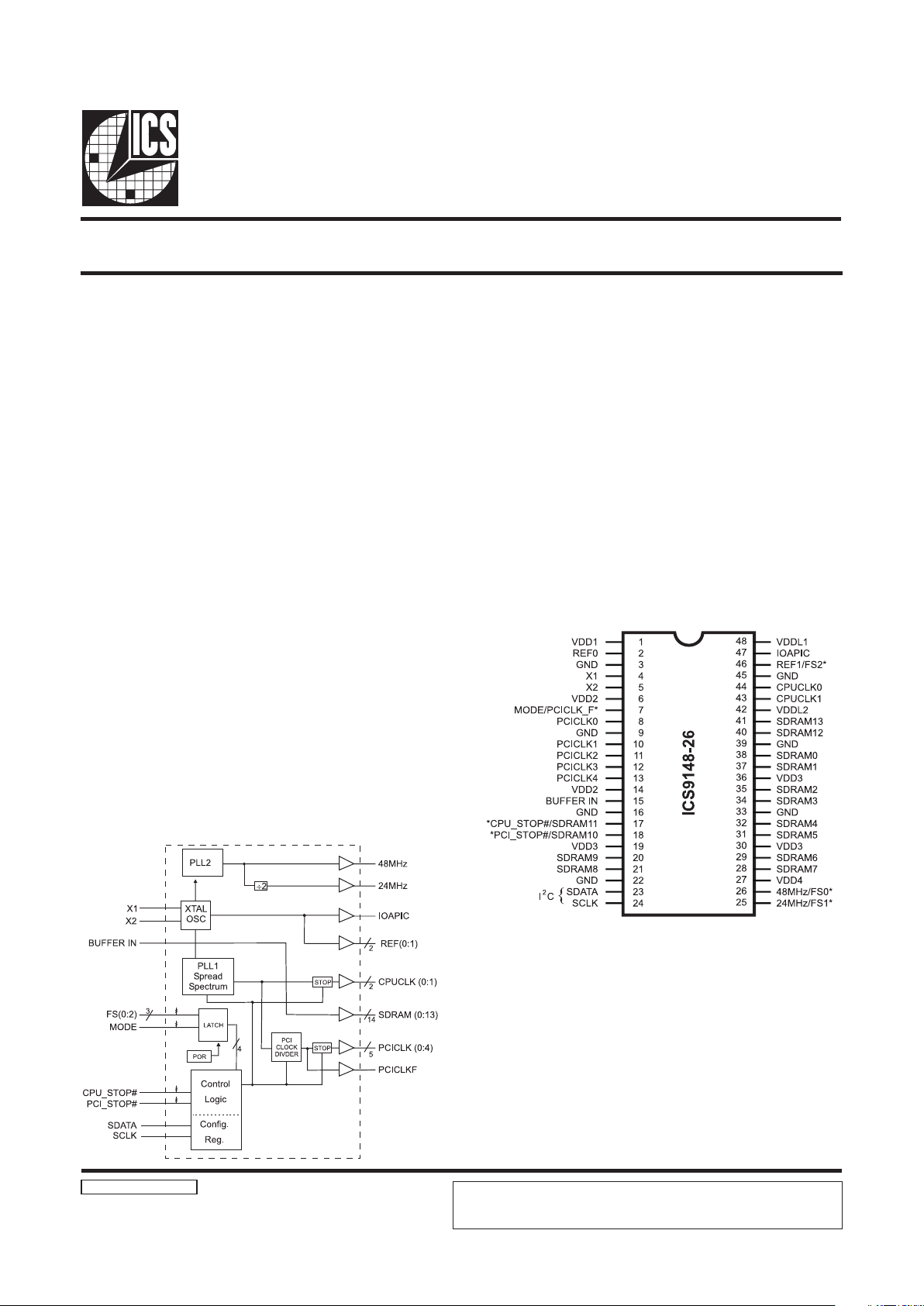
Block Diagram
Pentium is a trademark of Intel Corporation
I2C is a trademark of Philips Corporation
Frequency Generator & Integrated Buffers for PENTIUM/Pro
TM
9148-26 Rev D 07/23/98
Pin Configuration
3.3V outputs: SDRAM, PCI, REF, 48/24MHz
2.5V outputs: CPU, IOAPIC
20 ohm CPU clock output impedance
20 ohm PCI clock output impedance
Skew from CPU (earlier) to PCI clock - 1 to 4 ns, center 2.2 ns.
No external load cap for CL=18pF crystals
±250 ps CPU, PCI clock skew
250ps (cycle to cycle) CPU jitter @ 66.66MHz
Smooth frequency switch, with selections from 50 to
133 MHz CPU.
I2C interface for programming
2ms power up clock stable time
Clock duty cycle 45-55%.
48 pin 300 mil SSOP package
3.3V operation, 5V tolerant inputs (with series R)
<6ns propagation delay SDRAM form Buffer Input
48-Pin SSOP
Power Groups
VDD1 = REF (0:1), X1, X2
VDD2 = PCICLK_F, PCICLK(0:4)
VDD3 = SDRAM (0:13), supply for PLL core
VDD4 = 24MHz, 48MHz
VDDL1 = IOAPIC
VDDL2 = CPUCLK (0:1)
* Internal Pull-up Resistor of
240K to 3.3V on indicated inputs
The ICS9148-26 generates all clocks required for high speed
RISC or CISC microprocessor systems such as Intel PentiumPro
or Cyrix. Eight different reference frequency multiplying factors
are externally selectable with smooth frequency transitions.
Features include two CPU, six PCI and fourteen SDRAM clocks.
Two reference outputs are available equal to the crystal
frequency. Plus the IOAPIC output powered by VDDL1. One
48 MHz for USB, and one 24 MHz clock for Super IO. Spread
Spectrum built in at ±0.5% or ±1.5% modulation to reduce the
EMI. Serial programming I2C interface allows changing
functions, stop clock programing and Frequency selection.
Additionally, the device meets the Pentium power-up
stabilization, which requires that CPU and PCI clocks be stable
within 2ms after power-up. It is not recommended to use I/O
dual function pin for the slots (ISA, PIC, CPU, DIMM). The
add on card might have a pull up or pull down.
High drive PCICLK and SDRAM outputs typically provide
greater than 1 V/ns slew rate into 30pF loads. CPUCLK outputs
typically provide better than 1V/ns slew rate into 20pF loads
while maintaining 50±5% duty cycle. The REF and 24 and 48
MHz clock outputs typically provide better than 0.5V/ns slew
rates into 20pF.
ICS reserves the right to make changes in the device data identified in this
publication without further notice. ICS advises its customers to obtain the latest
version of all device data to verify that any information being relied upon by the
customer is current and accurate.
Page 2
2
ICS9148-26
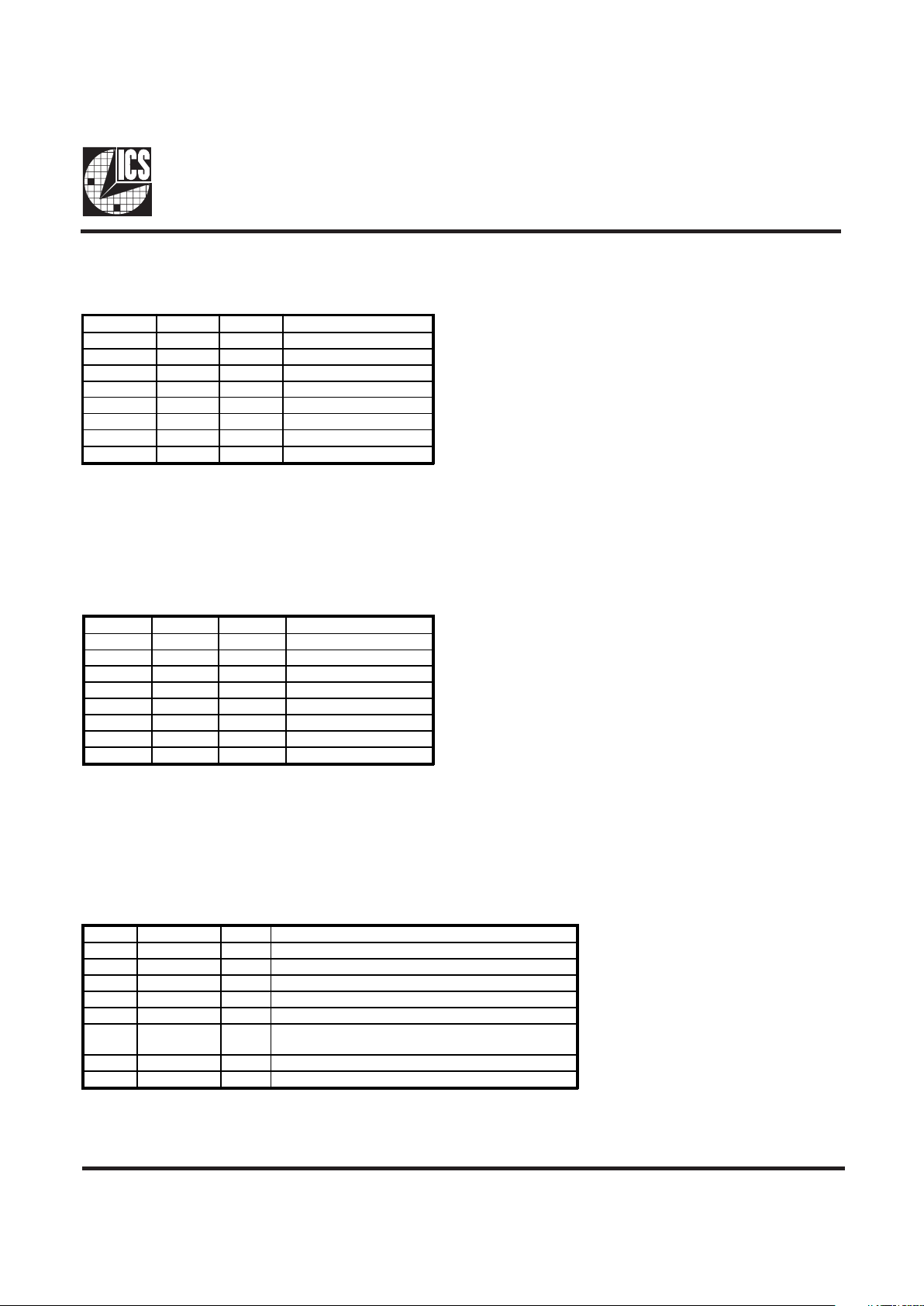
Pin Descriptions
Notes:
1: Internal Pull-up Resistor of 240K to 3.3V on indicated inputs
2: Bidirectional input/output pins, input logic levels are latched at internal power-on-reset. Use 10Kohm resistor
to program logic Hi to VDD or GND for logic low.
PIN NUMBER PIN NAME TYPE DESCRIPTION
1 VDD1 PW R Ref (0:2), XTAL power supply, nominal 3.3V
2REF0 OUT
14.318 Mhz reference clock. This REF output is the
STRONGER buffer for ISA BUS loads
3,9,16,22,
33,39,45
GND PW R Gr ound
4X1 IN
Crystal input, has internal load cap (36pF) and feedback
resistor from X2
5X2 OUT
Crystal output, nominally 14.318MHz. Has internal load
cap (36pF)
6,14 VDD2 PW R Supply fo r PCICLK_F and PCICLK (0:5), nominal 3.3V
7
PCICLK_F
OUT
Free running PCI clock
MODE
1, 2
IN
Pin 17, pin 18 function select pin, 1=Desktop Mode, 0=Mob ile
Mode. Latched Inp ut.
8
PCICLK0
OUT
PCI clock output.
10, 11, 12, 13
PCICLK(1:4)
OUT
PCI clock outputs.
15
BUFFER IN
IN
Input to Fanout Buffers for SDRAM outputs.
18
PCI_STOP#
1
IN
Halts PCICLK(0:4) clocks at logic 0 level, when input low (In
mobile mode, MODE =0)
17, 18, 20, 21,
28, 29, 31, 32,
34, 35,37,38,40,41
SDRAM (0:13)
OUT
(Pins 17, 18 SDRAM output only if MODE=High)
SDRAM clock outputs, Fanout Buffer outputs from BUFFER IN pin
(controlled by chipset).
19,30,36
VDD3
PWR
Supply for SDRAM (0:13) and CPU PLL Core, nominal 3.3V.
23
SDATA
IN
Data input for I2C serial input, 5V tolerant input
24
SCLK
IN
Clock input of I2C input, 5V tolerant input
25
24MHz
OUT
24MHz output clock
FS1
1, 2
IN
Frequency select pin. L atched Input.
26
48MHz
OUT
48MHz output clock
FS0
1, 2
IN
Frequency select pin. Latched Input
27
VDD4
PWR
Power for 24 & 4 8MHz output buffers and f ixed PLL core.
43, 44
CPUCLK(0:1)
OUT
CPU clock outputs, power ed by VDDL2. Low if CPU_STOP#=Low
42
VDDL2
PWR
Supply for CPU (0:1), eith er 2.5V or 3.3V nominal
46
REF1 OUT 14.318 MHz reference clock .
FS2
1, 2
IN
Frequency select pin. Latched Input
17 CPU_STOP#
1
IN
Halts CPUCLK (0:1) clocks at logic 0 level, when input low (in
Mobile Mode, MODE=0)
47 IOAPIC OUT IOAPIC clock output. 14.318 MHz Power ed by VDDL1.
48 VDD L1 PW R Supply for IOAPIC, either 2.5 or 3.3V nominal
Page 3
3
ICS9148-26
Functionality
VDD1,2,3 = 3.3V±5%, V
DDL
1,2 = 2.5V±5% or 3.3±5%, TA=0 to 70°C
Crystal (X1, X2) = 14.31818MHz
Power Management Functionality
Mode Pin - Power Management Input Control
MODE, Pin 7
(Latched Input)
Pin 17 Pin 18
0
CPU_STOP#
(INPUT)
PCI_STOP#
(INPUT)
1
SDRAM11
(OUTPUT)
SDRAM10
(OUTPUT)
FS2 FS1 FS0
CPU
(M Hz)
PCICLK
(M Hz)
REF, IO AP IC
(M Hz)
1 1 1 100.2 33.3 (CPU/3) 14 .31 8
1 1 0 133.3
1
33.3 (CPU/4)
1
14.318
1 0 1 112.0
1
37.3 (CPU/3)
1
14.318
1 0 0 103 34.3 (CPU/3) 14.318
0 1 1 66.8 33.4 (CPU/2) 14.318
0 1 0 83.3 41.65 (CPU/2) 14.318
0 0 1 75 37.5 (CPU/2) 14 .31 8
0 0 0 50 25 (CPU/2) 14.318
CPU_STOP# PCI_STOP#
CPUCLK
Outputs
PCICLK
(0:4)
PCICLK_F ,
REF ,
24/48MHz
and SDRAM
Crystal
OSC
VCO
0 1 Stopped Low Runni ng Running Running Running
1 1 Running Running Running Running Running
1 0 Running Stopped Low R unning Running Running
0 0 Stopped Low Stopp ed Low Runni ng R unning R unning
Note1. Performance not guaranteed
Page 4
4
ICS9148-26
Byte0: Functionality and Frequency Select Register (default = 0)
Serial Configuration Command Bitmap
A. For the clock generator to be addressed by an I2C controller, the following address must be sent as a start sequence, with
an acknoledge bit between each byte.
B. The clock generator is a slave/receiver I2C component. It can read back the data stored in the latches for verification. (set
R/W# to 1 above) Read-Back will support Intel PIIX4 "Block-Read" protocol, with a "Byte count" following the
address with R/W#=1, then proceding to Byte 0, 1, 2, ...until STOP.
C. The data transfer rate supported by this clock generator is 100K bits/sec (standard mode)
D. The input is operating at 3.3V logic levels.
E. The data byte format is 8 bit bytes.
F. To simplify the clock generator I2C interface, the protocol is set to use only "Block-Writes" from the controller. The
bytes must be accessed in sequential order from lowest to highest byte with the ability to stop after any complete byte
has been transferred. The Command code and Byte count shown above must be sent, but the data is ignored for those
two bytes. The data is loaded until a Stop sequence is issued.
G.. At power-on, all registers are set to a default condition. Byte 0 defaults to a 0, Bytes 1 through 5 default to a 1 (Enabled
output state).
General I2C serial interface information
I2C is a trademark of Philips Corporation
Then Byte 0, 1, 2, etc in
sequence until STOP.
Clock Generator
Address (7 bits)
ACK
+ 8 bits dummy
command code
ACK
+ 8 bits dummy
Byte count
ACK
A(6:0) & R/W#
D2
(H)
Then Byte 0, 1, 2, etc. in
sequence until STOP.
Clock Generator
Address (7 bits)
ACK
Byte Count
Readback
ACK
A(6:0) & R/W#
D3
(H)
Bit Description PWD
Bit 7
0 - ±1.5% S pread Spectrum M odulation
1 - ±0.5% Spread Spectrum Mo dulation
0
Bit6 Bit5 Bit4 CP U cloc k PC I
Note1
Bit 6:4
111
110
100.2
133.3
2
33.3 (CPU/3)
33.3
2
101
100
112.0
2
103
37.3
2
34.3 (CPU/3)
011
010
66.8
83.3
33.4 (CPU/2)
41.65(CPU/2)
001
000
75
50
37.5 (CPU/2)
25 (CPU/2)
Bit 3
0 - Frequency is selected by hardware select, Latched Inputs
1 - F requency is selected by Bit 6:4 (above)
0
Bit 2
0 - S pread Spectrum center spread type.
1 - S pread Spectrum down spread type.
0
Bit 1
0 - N ormal
1 - Spread Spectrum Enabled
0
Bit 0
0 - Running
1 - Trist at e all ou t pu t s
0
Note1. Default at Power-up will be for
latched logic inputs to define
frequency. Bits 4, 5, 6 are default
to 000, and if bit 3 is written to a 1
to use Bits 6:4, then these should
be defined to desired frequency at
same write cycle.
Note2. Performance not guaranteed
Note: PWD = Power-Up Default
Page 5
5
ICS9148-26
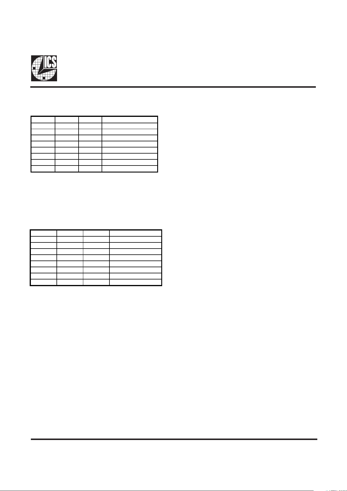
Byte 1: CPU, Active/Inactive Register (1 = enable, 0 = disable)
Byte 2: PCI Active/Inactive Register (1 = enable, 0 = disable)
Byte 3: SDRAM Active/Inactive Register (1 = enable, 0 = disable)
Notes:
1. Inactive means outputs are held LOW and are disabled from switching.
Notes:
1. Inactive means outputs are held LOW and are disabled from switching.
Notes:
1. Inactive means outputs are held LOW and are disabled from switching.
Bit Pin # PWD Description
Bit 7 - 1 (Reserved)
Bit 6 - 1 (Reserved)
Bit 5 - 1 (Reserved)
Bit 4 - 1 (Reserved)
Bit 3 40 1 SDRAM12 (Act/Inact)
Bit 2 41 1 SDRAM13 (Act/Inact)
Bit 1 43 1 CPUC LK1 (Act/I nact)
Bit 0 44 1 CPUC LK0 (Act/I nact)
Bit Pin # PWD Description
Bit 7 - 1 (Reserved)
Bit 6 7 1 PCICLK_F (Act/Inact)
Bit 5 - 1 (Reserved)
Bit 4 14 1 PCICLK4 (Act/Inact)
Bit 3 12 1 PCICLK3 (Act/Inact)
Bit 2 11 1 PCICLK2 (Act/Inact)
Bit 1 10 1 PCICLK1 (Act/Inact)
Bit 0 8 1 PCICLK0 (Act/Inact)
Bit Pin # PW D Description
Bit 7 - 1 (Reserved)
Bit 6 - 1 (Reserved)
Bit 5 26 1 48MHz (Act/Inact)
Bit 4 25 1 24 MHz (Act/Inact)
Bit 3 - 1 (Reserved)
Bit 2 21,20,18,17 1
SDRAM (8:11) (Active/Inactive)
(SDRAM 10, 11 only in Desktop Mode, MODE=1)
Bit 1 32,31,29,28 1 SDRAM (4:7) (Active/Inactive)
Bit 0 38,37,35,34 1 SDRAM (0:3) (Active/Inactive)
Page 6
6
ICS9148-26
Byte 4: Reserved Active/Inactive Register (1 = enable, 0 = disable)
Byte 5: Peripheral Active/Inactive Register (1 = enable, 0 = disable)
Notes:
1. Inactive means outputs are held LOW and are disabled from switching.
Notes:
1. Inactive means outputs are held LOW and are disabled from switching.
Bit Pin # PWD Description
Bit 7 - 1 (Reserved)
Bit 6 - 1 (Reserved)
Bit 5 - 1 (Reserved)
Bit 4 - 1 (Reserved)
Bit 3 - 1 (Reserved)
Bit 2 - 1 (Reserved)
Bit 1 - 1 (Reserved)
Bit 0 - 1 (Reserved)
Bit Pin # PWD Description
Bit 7 - 1 (Reserve d)
Bit 6 - 1 (Reserve d)
Bit 5 - 1 (Reserve d)
Bit 4 47 1 IOAPIC0 (Act/Inact)
Bit 3 - 1 (Reserve d)
Bit 2 - 1 (Reserve d)
Bit 1 46 1 REF1 (Act/Inact)
Bit 0 2 1 REF0 (Act/Inact)
Page 7

7
ICS9148-26
CPU_STOP# Timing Diagram
CPU_STOP# is an asychronous input to the clock synthesizer. It is used to turn off the CPU clocks for low power operation.
CPU_STOP# is synchronized by the ICS9148-26. The minimum that the CPU clock is enabled (CPU_STOP# high pulse) is 100
CPU clocks. All other clocks will continue to run while the CPU clocks are disabled. The CPU clocks will always be stopped in
a low state and start in such a manner that guarantees the high pulse width is a full pulse. CPU clock on latency is less than 4
CPU clocks and CPU clock off latency is less than 4 CPU clocks.
Notes:
1. All timing is referenced to the internal CPU clock.
2. CPU_STOP# is an asynchronous input and metastable conditions may exist. This signal is synchronized
to the CPU clocks inside the ICS9148-26.
3. All other clocks continue to run undisturbed.
4. SDRAM outputs are controlled by Buffer in signal, not affected by the ICS9148-26
CPU_STOP# signal.
Page 8

8
ICS9148-26
PCI_STOP# Timing Diagram
PCI_STOP# is an asynchronous input to the ICS9148-26. It is used to turn off the PCICLK (0:4) clocks for low power operation.
PCI_STOP# is synchronized by the ICS9148-26 internally. The minimum that the PCICLK (0:4) clocks are enabled (PCI_STOP#
high pulse) is at least 10 PCICLK (0:4) clocks. PCICLK (0:4) clocks are stopped in a low state and started with a full high pulse
width guaranteed. PCICLK (0:4) clock on latency cycles are only one rising PCICLK clock off latency is one PCICLK clock.
Notes:
1. All timing is referenced to the Internal CPUCLK (defined as inside the ICS9148 device.)
2. PCI_STOP# is an asynchronous input, and metastable conditions may exist. This signal is required to be synchronized
inside the ICS9148.
3. All other clocks continue to run undisturbed.
4. CPU_STOP# is shown in a high (true) state.
Page 9

9
ICS9148-26
Pins 7,25,26,46 on the ICS9148-26 serve as dual signal
functions to the device. During initial power-up, they act as
input pins. The logic level (voltage) that is present on these
pins at this time is read and stored into a 4-bit internal data
latch. At the end of Power-On reset, (see AC characteristics
for timing values), the device changes the mode of operations
for these pins to an output function. In this mode the pins
produce the specified buffered clocks to external loads.
To program (load) the internal configuration register for these
pins, a resistor is connected to either the VDD (logic 1)
power supply or the GND (logic 0) voltage potential. A 10
Kilohm(10K) resistor is used to provide both the solid CMOS
programming voltage needed during the power-up
programming period and to provide an insignificant load on
the output clock during the subsequent operating period.
Figs. 1 and 2 show the recommended means of implementing
this function. In Fig. 1 either one of the resistors is loaded
onto the board (selective stuffing) to configure the devices
internal logic. Figs. 2a and b provide a single resistor loading
option where either solder spot tabs or a physical jumper
header may be used.
Shared Pin Operation Input/Output Pins
Fig. 1
These figures illustrate the optimal PCB physical layout
options. These configuration resistors are of such a large
ohmic value that they do not effect the low impedance clock
signals. The layouts have been optimized to provide as little
impedance transition to the clock signal as possible, as it
passes through the programming resistor pad(s).
Page 10

10
ICS9148-26
Fig. 2a
Fig. 2b
Page 11

11
ICS9148-26
Absolute Maximum Ratings
Supply Voltage . . . . . . . . . . . . . . . . . . . . . . . . . . . 7.0 V
Logic Inputs . . . . . . . . . . . . . . . . . . . . . . . . . . . . GND 0.5 V to VDD +0.5 V
Ambient Operating Temperature . . . . . . . . . . . . 0°C to +70°C
Storage Temperature . . . . . . . . . . . . . . . . . . . . . . 65°C to +150°C
Stresses above those listed under Absolute Maximum Ratings may cause permanent damage to the device. These ratings are
stress specifications only and functional operation of the device at these or any other conditions above those listed in the
operational sections of the specifications is not implied. Exposure to absolute maximum rating conditions for extended periods
may affect product reliability.
Electrical Characteristics - Input/Supply/Common Output Parameters
TA = 0 - 70C; Supply Voltage VDD = 3.3 V +/-5% (unle ss otherw ise stated)
PARAMETER SYMBOL CONDITIONS MIN TY P MAX UNITS
Input High Vol t a ge V
IH
2V
DD
+0.3 V
In put Low Voltage V
IL
VSS-0.3 0.8 V
Supply C urrent I
DD
CL = 0 pF; Select @ 66M 77 180 mA
I
DDL
6.0 30 mA
Input frequenc y F
i
VDD = 3.3 V; 14.318 MHz
Input Capacitance
1
C
IN
Logic Inputs 5 pF
C
INX
X1 & X2 pins 27 36 45 pS
Transition Tim e
1
T
trans
To 1st cr ossi ng of targe t Fr e q. 1 .5 3 m S
Settling Time
1
T
s
From 1st crossing to 1% ta rget Freq. mS
Clk Stabilization
1
T
STAB
From VDD = 3.3 V to 1% target Freq. 3 mS
Skew
1
T
CPU-BUSVT
= 1.5 V;
1.0 2.2 4.0 nS
1
Guare nteed by design, not 100% tested in pr od uc t ion.
Page 12

12
ICS9148-26
Electrical Characteristics - CPU
TA = 0 - 70C; VDD = 3.3 V +/-5%; V
DDL
= 2.5 V +/-5%; CL = 20 pF ( unless otherwise state d)
PARAMETER SYMBOL CONDITIONS MIN TY P MAX UNITS
O utp ut Im pedance R
DSP2A
1
VO = VDD*(0.5) 10 20
Ω
O utp ut Im pedance R
DSN2A
1
VO = VDD*(0.5) 10 20
Ω
O utput High Voltage V
OH2BIOH
= -12.0 mA 2 2.3 V
Output Low V oltage V
OL2BIOL
= 12 mA 0.2 0.4 V
Ou tput High Current I
OH2B
VOH = 1.7 V -41 -19 mA
Output Low Current I
OL2B
VOL = 0.7 V 19 37 m A
Rise Time t
r2A
1
VOL = 0.4 V, VOH = 2.0 V 1.3 2.1 nS
Fall Time t
f2A
1
VOH = 2.0 V , VOL = 0.4 V 1.0 2.0 nS
Duty Cycle d
t2A
1
VT = 1.25 V 45.0 51.0 55.0 %
Skew
(Window)
t
sk2A
1
VT = 1.25 V 120 250 pS
period(norm) V
T
= 1.25 V ; 100MHz 9.75 10 10.25 nS
period(spr) V
T
= 1.25 V ; 100MHz 9.75 10 10.35 nS
Jitter t
j1s2A
1
VT = 1.25 V 120 350 pS
t
jabs2A
1
VT = 1.25 V -250 100 +250
Dev run avg
V
T
= 1.25 V
150 250 pS
1
Guare nt eed by design, not 100% teste d in produc tion.
Page 13

13
ICS9148-26
Electrical Characteristics - 24M, 48M, REF 1
TA = 0 - 70C; VDD = V
DDL
= 3.3 V +/-5%; CL = 20 pF ( unless otherwise state d)
PARAMETER SYMBOL CONDITIONS MIN TY P MAX UNITS
O utp ut Im pedance R
DSP5
1
VO = VDD*(0.5) 20 60 W
O utp ut Im pedance R
DSN5
1
VO = VDD*(0.5) 55 100 W
O utput High Voltage V
OH5
IOH = -14 mA 2.4 2.9 V
Output Low V oltage V
OL5
IOL = 6.0 mA 0.25 0.4 V
Ou tput High Current I
OH5
VOH = 2.0 V -42 -20 mA
Output Low Current I
OL5
VOL = 0.8 V 10 18 m A
Rise Time t
r5
1
VOL = 0.8 V, VOH = 2.4 V 1.1 2.0 nS
Fall Time t
f5
1
VOH = 2.4 V , VOL = 0.8 V 1.0 2.5 nS
Duty Cycle d
t5
1
VT = 1.5 V 40.0 52.0 60.0 %
Jitter t
j1s5
1
VT = 1.5 V 100 250 pS
t
jabs5
1
VT = 1.5 V
250 800 pS
1
Guare nt eed by design, not 100% teste d in production.
Page 14

14
ICS9148-26
Electrical Characteristics - BUS
TA = 0 - 70C; VDD = 3.3 V +/-5%; CL = 30 pF (unless otherwise stat e d)
PARAMETER SYMBOL CONDITIONS MIN TY P MAX UNITS
O utp ut Im pedance R
DSP1
1
VO = VDD*(0.5) 12 23 55
Ω
O utp ut Im pedance R
DSN1
1
VO = VDD*(0.5) 12 20 55
Ω
O utput High Voltage V
OH1
IOH = -18 mA 2.4 2.9 V
Output Low V oltage V
OL1
IOL = 9.4 mA 0.2 0.4 V
Ou tput High Current I
OH1
VOH = 2.0 V -58 -22 mA
Output Low Current I
OL1
VOL = 0.8 V 25 52 m A
Rise Time t
r1
1
VOL = 0.8 V, VOH = 2.4 V 1.5 2.0 nS
Fall Time t
f1
1
VOH = 2.4 V , VOL = 0.8 V 1.4 2.5 nS
Duty Cycle d
t1
1
VT = 1.5 V 45.0 50.0 55.0 %
Skew t
sk1
1
VT = 1.5 V 80 250 pS
Jitter t
j1s1
1
VT = 1.5 V 50 150 pS
t
jabs1
1
VT = 1.5 V
200 500 pS
1
Guare nt eed by design, not 100% teste d in produc tion.
Page 15

15
ICS9148-26
Electrical Characteristics - SDRAM
TA = 0 - 70C; VDD =V
DDL
3.3 V +/-5%; CL = 30 pF (unl e ss otherwise stated)
PARAMETER SYMBOL CONDITIONS MIN TY P MAX UNITS
O utput Im pe da nc e R
DSP2A
1
VO = VDD*(0.5) 10 20
Ω
O utput Im pe da nc e R
DSN2A
1
VO = VDD*(0.5) 10 20
Ω
O utput High Volta ge V
OH2AIOH
= -28 mA 2.4 2.8 V
O utput Low Vol ta ge V
OL2AIOL
= 19 m A 0.3 0.4 V
O utput High C urrent I
OH2A
VOH = 2.0 V -72 -42 mA
O utput Low Curre nt I
OL2A
VOL = 0.8 V 33 50 mA
Rise Time t
r2A
1
VOL = 0.8 V, VOH = 2.4 V 1.1 2.0 nS
Fall Ti me t
f2A
1
VOH = 2.4 V , VOL = 0.8 V 1.5 2.5 nS
Duty Cycle d
t2A
1
VT = 1.5 V 55 65 75 %
Skew ( output to output ) t
sk2A
1
VT = 1.5 V 200 600 pS
Skew ( Buff e rin to output )
t
sk2A
1
VT = 1.5 V
5.5 7.0 nS
1
Guarenteed by design, not 100% tested in production.
Page 16

16
ICS9148-26
General Layout Precautions:
1) Use a ground plane on the top layer
of the PCB in all areas not used by
traces.
2) Make all power traces and vias as
wide as possible to lower inductance.
Notes:
1 All clock outputs should have series
terminating resistor. Not shown in all
places to improve readibility of
diagram
2 Optional EMI capacitor should be
used on all CPU, SDRAM, and PCI
outputs.
3 Optional crystal load capacitors are
recommended.
Capacitor Values:
C1, C2 : Crystal load values determined by user
C3 : 100pF ceramic
All unmarked capacitors are 0.01µF ceramic
Page 17

17
ICS9148-26
SSOP Package
Ordering Information
ICS9148F-26
Pattern Number (2 or 3 digit number for parts with ROM code patterns)
Package Type
F=SSOP
Device Type (consists of 3 or 4 digit numbers)
Prefix
ICS, AV = Standard Device
Example:
ICS XXXX F - PPP
SYMB OL COM MON DIMENSIONS VARIATIONS D N
MIN. NOM. MAX. MIN. NOM. MAX.
A .095 .101 .110 AC .620 .625 .630 48
A1 .00 8 .012 .01 6
A2 .08 8 .090 .09 2
B .008 .010 .0135
C.005- .010
D See Variations
E .292 .296 .299
e0.025 BSC
H .400 .406 .410
h .010 .013 .016
L .024 .032 .040
N See Variations
∝
0° 5° 8°
X .085 .093 .100
ICS reserves the right to make changes in the device data identified in this
publication without further notice. ICS advises its customers to obtain the latest
version of all device data to verify that any information being relied upon by the
customer is current and accurate.
 Loading...