

Page 1
Integrated
Circuit
Systems, Inc.
General Description Features
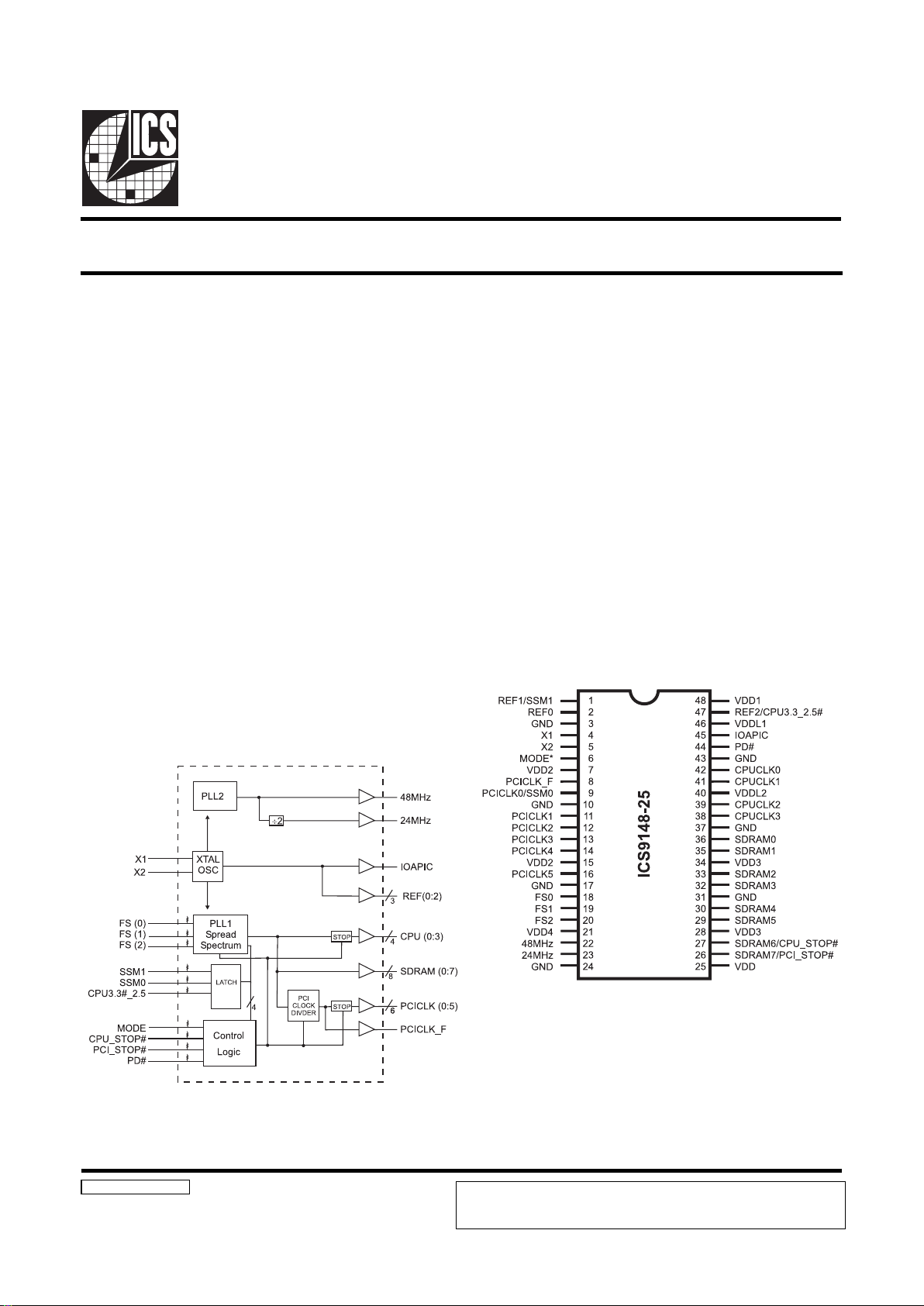
ICS9148-25
Block Diagram
Pentium/ProTM System and Cyrix™ Clock Chip
9148-25 Rev B 5/20/99
Pin Configuration
48-Pin SSOP
Pentium is a trademark on Intel Corporation.
• Generates system clocks for CPU, IOAPIC, SDRAM,
PCI, plus 14.318 MHz ), USB, Plus Super I/O
• Spread spectrum for CPU/SDRAM/PCI clocks default
• Supports single or dual processor systems
• Modulation of Spread Spectrum selectable as ±0.5, ±1.0,
±2.0 or none
• Supports Intel 60, 66.8MHz, Cyrix 55, 75MHz plus 83.3
and 68MHz (Turbo of 66.6) speeds.
• Synchronous clocks skew matched to 250ps window on
CPU, SDRAM and 500ps window on PCI clocks
• CPU clocks to PCI clocks skew 1-4ns (CPU early)
• MODE input pin selects optional power management
input control pins
• T wo fixed outputs, 48MHz and 24 MHz
• Separate 2.5V and 3.3V supply pins
- 2.5V or 3.3V output: CPU, IOAPIC (Strength
selectable)
- 3.3V outputs: SDRAM, PCI, REF , 48/24 MHz
• No power supply sequence requirements
• 48 pin 300 mil SSOP
The ICS9148-25 is a Clock Synthesizer chip for Pentium and
PentiumPro plus Cyrix CPU based Desktop/Notebook systems
that will provide all necessary clock timing.
Features include four CPU, seven PCI and eight SDRAM
clocks. T wo reference outputs are available equal to the crystal
frequency, plus the IOAPIC output powered by VDDL.
Additionally, the device meets the Pentium power-up
stabilization, which requires that CPU and PCI clocks be stable
within 2ms after power-up.
High drive PCICLK and SDRAM outputs typically provide
greater than 1 V/ns slew rate into 30pF loads. CPUCLK outputs
typically provide better than 1V/ns slew rate into 20pF loads
while maintaining 50 ±5% duty cycle. The REF clock outputs
typically provide better than 0.5V/ns slew rates.
The ICS9148-25 accepts a 14.318MHz reference crystal or
clock as its input and runs on a 3.3V supply.
Sperad Spectrum is modulated in center-spread mode on CPU/
SDRAM/PCI clocks. Modulation amount is selectable at
power-up (latched inputs) for ±0.5, ±1.0, ±2.0 or No spreading.
Power Groups
VDD = Supply for PLL core.
VDD1 = REF (0:2), X1, X2
VDD2 = PCICLK_F , PCICLK (0:5)
VDD3 = SDRAM (0:5), SDRAM6/CPU_STOP#,
SDRAM7/PCI_STOP#
VDD4 = 48MHz, 24MHz
VDDL1 = IOAPIC
VDDL2 = CPUCLK (0:3)
ICS reserves the right to make changes in the device data identified in this
publication without further notice. ICS advises its customers to obtain the latest
version of all device data to verify that any information being relied upon by the
customer is current and accurate.
Page 2
2
ICS9148-25
Pin Descriptions
Functionality
REBMUNNIPEMANNIPEPYTNOITPIRCSED
1
1MSSNI
tnuomanoitaludommurtcepSdaerpSroftupnidehctaL
*)elbatees(
1FERTUOtuptuokcolcecnerefeR
20FERTUOtuptuokcolcecnerefeR
,42,71,01,3
34,73,13
DNGRWP)nommoc(dnuorG
41XNI
sedulcnI.zHM813.41yllanimon,tupniecnereferrolatsyrC
.2XmorfrotsiserkcabdeefdnaDNGotpacdaollanretni
52XTUO.DNGotpacdaollanretnisedulcni,tuptuolatsyrC
6EDOMNI*sniptnemeganaMrewoProfnoitcelesnoitcnuftupnI
51,72DDVRWP)5:0(KLCICPdna,F_KLCICProfylppuS
8F_KLCICPTUO#POTS_ICPybdetceffaton,kcolcICPgninnureerF
9
0KLCICPTUOskcolcICP
0MSSNI
tnuomanoitaludommurtcepSdaerpSroftupnidehctaL
*)elbatees(
61,41,31,21,11)5:1(KLC_ICPTUOskcolcICP
810SFNI*tupni0tcelesycneuqerF
911SFNI*tupni1tcelesycneuqerF
022SFNI*tupni2tcelesycneuqerF
124DDVRWPskcolczHM42dnazHM84rofylppuS
22zHM84TUOkcolcBSUroftuptuorevirdzHM84
32zHM42TUOO/IrepuSroftuptuorevirdzHM42
52DDVRWPerocLLProfylppuS
62
7MARDSTUOkcolcMARDS
#POTS_ICPNI*wolnehwlevel"0"cigoltxenta)5:0(suBICPstlaH
72
6MARDSTUOkcolcMARDS
#POTS_UPCNI*wolnehwlevel"0"cigoltxentaskcolcUPCstlaH
43,823DDVRWP
,#POTS_UPC/6MARDS,)5:0(MARDSrofylppuS
POTS_ICP/7MARDS
63,53,33,23,03,92)5:0(MARDSTUOdeepsUPCtakcolcsMARDS
24,14,93,83)3:0(KLCUPCTUO2LDDVybderewop,tuptuokcolcKLCUPC
042DDVRWP)3:0(KLCUPCrofylppuS
44#DPNI*wolevitca,pihcnwodsrewoP
54CIPAOITUO
latsyrcta,1LDDVybderewop,tuptuokcolcCIPAOI
ycneuqerf
641LDDVRWPCIPAOIrofylppuS
74
#5.2_3.3UPCNI)elbatees(*noitceleshtgnertsreffubDDV5.2ro3.3dehctaL
2FERTUOtuptuokcolcecnerefeR
841DDVRWP2X,1X,)2:0(FERrofylppuS
*Internal pull-up resistor of 120 to 150K to 3.3V on indicated inputs.
VDD = 3.3V ±5% V
DDL
= 2.5V ±5% or 3.3V ±5%, TA = 0 to 70°C
Crystal (X1, X2) = 14.31818 MHz
2SF1SF0SF
,KLCUPC
MARDS
)zHM(
KLCICP
)zHM(
000 3.38UPC2/1
001 57)5.2/UPC(03
010 3.38)5.2/UPC(3.33
011 5.86UPC2/1
100 55UPC2/1
101 57UPC2/1
110 06UPC2/1
111 8.66UPC2/1
Page 3
3
ICS9148-25
6niP,EDOM62niP72niP
0
#POTS_ICP
tupnI
#POTS_UPC
tupnI
1tuptuO7MARDS
6MARDS
tuptuO
Mode Pin - Power Management Input Control
Power Management Functionality
#POTS_UPC#POTS_ICP#DP
KLCUPC
stuptuO
)5:0(KLCICP
stuptuO
,F_KLCICP
,FER
zHM84/42
MARDSdna
latsyrC
CSO
OCV
XX 0 woLdeppotSwoLdeppotSwoLdeppotSffOffO
00 1 woLdeppotSwoLdeppotSgninnuRgninnuRgninnuR
01 1 woLdeppotSgninnuRgninnuRgninnuRgninnuR
10 1 gninnuRwoLdeppotSgninnuRgninnuRgninnuR
11 1 gninnuRgninnuRgninnuRgninnuRgninnuR
Spread Spectrum Functionality
CPU 3.3_2.5V Buffer selector for CPUCLK and IOAPIC drivers.
#5.2_3.3UPC
leveLtupnIdehctaL
rofdetceleSreffuB
:tanoitarepO
0DDVV5.2
1DDVV3.3
1niPdehctaL
1MSS
9niPdehctaL
0MSS
MARDS,UPC
SKCOLCICPdna
CIPAOI,FERzHM42zHM84
00
ydaets,lamroN
edomycneuqerf
zHM813.41zHM42zHM84
01
nidetaludomycneuqerF
%0.2±daerpsretnec
zHM813.41zHM42zHM84
10
nidetaludomycneuqerF
%0.1±daerpsretnec
zHM813.41zHM42zHM84
*1*1
nidetaludomycneuqerF
%5.0±daerpsretnec
zHM813.41zHM42zHM84
*default with internal pull-ups
Page 4

4
ICS9148-25
T echnical Pin Function Descriptions
VDD(1,2,3,4)
This is the power supply to the internal core logic of the
device as well as the clock output buffers for REF(0:1),
PCICLK, 48/24MHzA/B and SDRAM(0:7).
This pin operates at 3.3V volts. Clocks from the listed buffers
that it supplies will have a voltage swing from Ground to this
level. For the actual guaranteed high and low voltage levels
for the Clocks, please consult the DC parameter table in this
data sheet.
VDDL1,2
This is the power supplies for the CPUCLK and IOAPCI
output buffers. The voltage level for these outputs may be
2.5 or 3.3volts. Clocks from the buffers that each supplies will
have a voltage swing from Ground to this level. For the actual
Guaranteed high and low voltage levels of these Clocks,
please consult the DC parameter table in this Data Sheet. See
control pin CPUCLK3.3_2.5# for output buffer strength
matching VDDL required for skew control.
GND
This is the power supply ground (common or negative) return
pin for the internal core logic and all the output buffers.
X1
This input pin serves one of two functions. When the device
is used with a Crystal, X1 acts as the input pin for the
reference signal that comes from the discrete crystal. When
the device is driven by an external clock signal, X1 is the
device input pin for that reference clock. This pin also
implements an internal Crystal loading capacitor that is
connected to ground. See the data tables for the value of this
capacitor. Also includes feedback resistor from X2.
X2
This Output pin is used only when the device uses a Crystal
as the reference frequency source. In this mode of operation,
X2 is an output signal that drives (or excites) the discrete
Crystal. The X2 pin will also implement an internal Crystal
loading capacitor that is connected to ground. See the Data
Sheet for the value of this capacitor.
CPUCLK (0:3)
These Output pins are the Clock Outputs that drive processor
and other CPU related circuitry that requires clocks which are
in tight skew tolerance with the CPU clock. The voltage
swing of these Clocks are controlled by the Voltage level
applied to the VDDL2 pin of the device. See the Functionality
Table for a list of the specific frequencies that are available
for these Clocks and the selection codes to produce them.
See control pin CPUCLK3.3_2.5# for output buffer strength
matching VDDL required for CPU to SDRAM skew control.
These clocks are modulated by Sperad Spectrum.
SDRAM(0:7)
These Output Clocks are use to drive Dynamic RAM’s and
are low skew copies of the CPU Clocks. The voltage swing of
the SDRAM’s output is controlled by the supply voltage
that is applied to VDD3 of the device, operates at 3.3 volts.
These clocks are modulated by Sperad Spectrum.
48MHz
This is a fixed frequency Clock output at 48MHz that is
typically used to drive USB devices.
24MHz
This pin is a fixed frequency clock output typically used to
drive Super I/O devices.
IOAPIC
This Output is a fixed frequency Output Clock that runs at
the Reference Input (typically 14.31818MHz) . Its voltage
level swing is controlled by VDDL1 and may operate at 2.5 or
3.3volts.
REF(0:2)
The REF Outputs are fixed frequency Clocks that run at the
same frequency as the Input Reference Clock X1 or the
Crystal (typically 14.31818MHz) attached across X1 and X2.
PCICLK_F
This Output is equal to PCICLK(0:5) and is FREE RUNNING,
and will not be stopped by PCI_STP#. This clock is modulated
by Spread Spectrum.
PCICLK (0:5)
These Output Clocks generate all the PCI timing requirements
for a Pentium/Pro based system. They conform to the current
PCI specification. They run at 1/2 CPU frequency , or CPU/2.5,
see frequency table. These clocks are modulated by Sperad
Spectrum.
FS (0,1,2)
These Input pins control the frequency of the Clocks at the
CPU, PCICLK and SDRAM output pins. See frequency table.
These pins are all Full-time inputs with a pull-up to VDD.
MODE
This Input pin is used to select the Input function of the
Power Management I/O pins 26 and 27. An active Low will
place pins in the Input mode and enable those stop clock
functions. This pin is a full-time input with a pull-up to VDD.
Page 5

5
ICS9148-25
CPU3.3_2.5#
This Input pin controls the CPU and IOAPIC output buffer
strength for skew matching CPU and SDRAM outputs to
compensate for the external VDDL supply condition. It is
important to use this function when selecting power supply
requirements for VDDL1,2. A logic “0” (ground) will indicate
2.5V operation and a logic “1” will indicate 3.3V operation.
This pin has an internal pull-up to VDD. This pin is a latched
input.
PD#
This is an asynchronous active Low Input pin used to Power
Down the device into a Low Power state by not removing the
power supply. The internal Clocks are disabled and the VCO
and Crystal are stopped. Powered Down will also place all the
Outputs in a low state at the end of their current cycle. The
latency of Power Down will not be greater than 3ms. This pin
is a Full-time input with a pull-up to VDD.
CPU_STOP#
This is a active Low Input pin used to stop the CPUCLK
clocks in an active low state. All other clocks will continue to
run while this function is enabled. The CPUCLK’ s will have a
turn OFF latency and a turn ON latency of 2 or 3 CPU clocks.
This pin is a Full-time input with a pull-up to VDD.
PCI_STOP#
This is a synchronous active Low Input pin used to stop the
PCICLK (0:5) clocks in a low state. It will not effect PCICLK_F
or any other outputs. There is only one full PCI clock output
for Turn OFF or Turn ON latency . This pin is a Full-time input
with a pull-up to VDD.
T echnical Pin Function Descriptions
SSM (0:1)
These pins define the input condition for the Spread Spectrum
amount of modulation. See Spread Spectrum functionality
table. Note that spreading is only done on the CPU/SDRAM/
PCI clocks no modulation is done on the REF, IOAPIC or
PLL2 (24, 48MHz) outputs.
These latched input pins are defined at power-on for logic Hi
or logic Low condition by external pull-up or pull-down
resistors, or the internal pull-up resistor to VDD. See shared
pin operation of Input/output pins on next page.
Page 6

6
ICS9148-25
Pins 1, 9 & 47 on the ICS9148-25 serve as dual signal
functions to the device. During initial power-up, they act as
input pins. The logic level (voltage) that is present on these
pins at this time is read and stored into a 4-bit internal data
latch. At the end of Power-On reset, (see AC characteristics
for timing values), the device changes the mode of operations
for these pins to an output function. In this mode the pins
produce the specified buffered clocks to external loads.
To program (load) the internal configuration register for these
pins, a resistor is connected to either the VDD (logic 1)
power supply or the GND (logic 0) voltage potential. A 10
Kilohm(10K) resistor is used to provide both the solid CMOS
programming voltage needed during the power-up
programming period and to provide an insignificant load on
the output clock during the subsequent operating period.
There is no degradation to the output clocks from resistors
as low as 2K ohm. The internal pull-up resistors can be used
as the logic high program input.
Shared Pin Operation Input/Output Pins
Fig. 1
Figs. 1 and 2 show the recommended means of implementing
this function. In Fig. 1 either one of the resistors is loaded
onto the board (selective stuffing) to configure the device’s
internal logic. Figs. 2a and b provide a single resistor loading
option where either solder spot tabs or a physical jumper
header may be used.
These figures illustrate the optimal PCB physical layout
options. These configuration resistors are of such a large
ohmic value that they do not effect the low impedance clock
signals. The layouts have been optimized to provide as little
impedance transition to the clock signal as possible, as it
passes through the programming resistor pad(s).
Page 7

7
ICS9148-25
Fig. 2a
Fig. 2b
Page 8

8
ICS9148-25
Electrical Characteristics - Input/Supply/Common Output Parameters
TA = 0 - 70C; S upply Voltage VDD = V
DDL
= 3.3 V + /-5% ( unless otherwise stated)
PARAMETER SYMBOL CONDITIONS MIN TYP MAX UNITS
Input High Voltage V
IH
2V
DD
+0.3 V
In put Low Voltage V
IL
VSS-0.3 0.8 V
Input High Current I
IH
VIN = V
DD
0.1 5
µ
A
Input Low Current I
IL1
VIN = 0 V; Inpu ts with no pull -up re sistors -5 2 .0
µ
A
Input Low Current I
IL2
VIN = 0 V; Inpu ts with pull -up re sistors -200 -100
µ
A
Operating I
DD3.3OPCL
= 0 pF; Select @ 66M 75 95 mA
Supply Curr ent
Power Down I
DD3.3PDCL
= 0 pF; With i np ut address to Vdd or GND 8 600
µ
A
Supply Curr ent
Input freque nc y F
i
VDD = 3.3 V ; 14.318 MHz
Input Capacitance
1
C
IN
Logic Inputs 5 pF
C
INX
X1 & X2 pins 27 36 45 pF
Transi ti on Time
1
T
tran s
To 1st c rossing of target F req. 3 ms
Settling Time
1
T
s
From 1 st cr ossing to 1% target Freq. 5 ms
Clk Stabilization
1
T
STAB
From VDD = 3.3 V to 1% target Freq. 3 ms
T
CPU-SDRAM1VT
= 1.5 V 200 500 ps
Skew
1
T
CPU-PCI1VT
= 1.5 V; 1 2 4.5 ns
T
REF-IOAPICVT
= 1.5 V;
900 ps
1
Guarenteed by design, not 100% tested in produ c t ion.
Electrical Characteristics - Input/Supply/Common Output Parameters
TA = 0 - 70C; S upply Vol t a ge VDD = 3.3 V +/-5%, V
DDL
= 2.5 V +/-5% (unless otherwise stated)
PARAMETER SYMBOL CONDITIONS MIN TYP MAX UNITS
Operating I
DD2.5OPCL
= 0 pF; Select @ 66M 8 9.5 mA
Supply Curr ent
T
CPU-SDRAM2VT
= 1.5 V; VTL = 1.25 V; SDRAM Leads 250 50 0 ps
Skew
1
T
REF-IOAPICVT
= 1.5 V; VTL = 1.25 V ; SDRAM Leads 260 ps
T
CPU-PCI2VT
= 1.5 V; VTL = 1.25 V ; CPU Leads
124ns
1
Guarente e d by de sign, not 100% tested in produ c t ion.
Page 9

9
ICS9148-25
Electrical Characteristics - CPU
TA = 0 - 70C; VDD = 3.3 V +/-5%, V
DDL
= 2.5 V +/-5%; CL = 10 - 20 pF (unle ss otherwise stat ed)
PARAMETER SYMBOL CONDITIONS MIN TYP MAX UNITS
O ut put Impedance R
DSP2B
1
VO = VDD*(0.5) 10 25
Ω
O ut put Impedance R
DSN2B
1
VO = VDD*(0.5) 10 25
Ω
O utput High Voltage V
OH2BIOH
= -13.0 mA 2 2.2 V
Output Low Voltage V
OL2BIOL
= 14 mA 0.3 0.4 V
Ou t put Hi gh Current I
OH2B
VOH = 1.7 V -25 -16 mA
Output Low C urrent I
OL2B
VOL = 0.7 V 22 26 mA
Rise Time t
r2B
1
VOL = 0.4 V, VOH = 2.0 V 1.35 1.6 ns
Fall Time t
f2B
1
VOH = 2.0 V , VOL = 0.4 V 1.2 1.6 ns
Duty Cycle d
t2B
1
VT = 1.25 V 45 50 55 ns
Skew t
sk2B
1
VT = 1.25 V 60 250 ps
t
jcyc-cyc2B
1
VT = 1.25 V 150 250 ps
Jitter t
j1s2B
1
VT = 1.25 V 30 150 ps
t
jabs2B
1
VT = 1.25 V
-250 80 +250 ps
1
Guarenteed by design, not 100% tested in produ c t ion.
Electrical Characteristics - PCI
TA = 0 - 70C; VDD = V
DDL
= 3. 3 V +/-5% ; CL = 30 pF (unles s othe rwis e s tate d)
PARA METER SY MBOL CON DI TION S MIN TY P MAX UN ITS
O utput Impeda nc e R
DSP1
1
VO = VDD*(0.5) 12 55
Ω
O utput Impeda nc e R
DSN1
1
VO = VDD*(0.5) 12 55
Ω
Output High Voltage V
OH1
IOH = -11 mA 2.6 3.1 V
Output Low Voltage V
OL1
IOL = 9. 4 mA 0.15 0. 4 V
O utput High Curr e nt I
OH1
VOH = 2 . 0 V -62 -40 m A
O utput L o w Current I
OL1
VOL = 0. 8 V 40 55 mA
Rise Time t
r1
1
VOL = 0. 4 V, VOH = 2.4 V 1.5 2 ns
F all T ime t
f1
1
VOH = 2. 4 V, VOL = 0.4 V 1.4 2 ns
Duty Cycle d
t1
1
VT = 1.5 V 455060%
Skew t
sk1
1
VT = 1. 5 V 200 500 ps
Jitte r t
j1s1
1
VT = 1. 5 V 10 150 ps
t
jabs1
1
VT = 1. 5 V
-250 65 250 ps
1
G uarenteed by de s ign, not 100% tes te d in production.
Page 10

10
ICS9148-25
Electrical Characteristics - SDRAM
TA = 0 - 70C; VDD = V
DDL
= 3.3 V +/-5%; CL = 20 - 30 pF (unless otherwise stated)
PARAMETER SYMBOL CONDITIONS MIN TYP MAX UNITS
O ut put Impedance R
DSP3
1
VO = VDD*(0.5) 10 24
Ω
O ut put Impedance R
DSN3
1
VO = VDD*(0.5) 10 24
Ω
O utput High Voltage V
OH3
IOH = -30 mA 2.6 2.8 V
Output Low Voltage V
OL3
IOL = 23 mA 0.3 0.4 V
Ou t put Hi gh Cur rent I
OH3
VOH = 2.0 V -62 -40 mA
Output Low C urrent I
OL3
VOL = 0.8 V 40 55 mA
Rise Time T
r3
1
VOL = 0.4 V, VOH = 2.4 V 1.5 2 ns
Fall Time T
f3
1
VOH = 2.4 V, VOL = 0.4 V 1.4 2 ns
Duty Cycle D
t3
1
VT = 1.5 V 45 50 60 %
Skew T
sk3
1
VT = 1.5 V 200 500 ps
Jitter T
j1s3
1
VT = 1.5 V 50 150 ps
T
jabs3
1
VT = 1.5 V
-250 100 250 ps
1
Guarenteed by design, not 100% tested in produ c t ion.
Electrical Characteristics - IOAPIC
TA = 0 - 70C; VDD = 3.3 V +/-5%, V
DDL
= 2.5 V +/-5%; CL = 10 - 20 pF (unle ss otherwise sta ted)
PARAMETER SYMBOL CONDITIONS MIN TYP MAX UNITS
O ut put Impedance R
DSP4B
1
VO = VDD*(0.5) 10 30
Ω
O ut put Impedance R
DSN4B
1
VO = VDD*(0.5) 10 30
Ω
O utput High Voltage V
OH4\BIOH
= -8 mA 2 2.5 V
Output Low Voltage V
OL4BIOL
= 12 mA 0.3 0.5 V
Ou t put Hi gh Current I
OH4B
VOH = 1.7 V -25 -16 mA
Output Low C urrent I
OL4B
VOL = 0.7 V 19 23 mA
Rise Time t
r4B
1
VOL = 0.4 V, VOH = 2.0 V 1.4 1.6 ns
Fall Time t
f4B
1
VOH = 2.0 V, VOL = 0.4 V 1.2 1.6 ns
Duty Cycle d
t4B
1
VT = 1.25 V 40 53 60 %
t
jcyc-cyc4B
1
VT = 1.25 V 1400 ps
Jitter t
j1s4B
1
VT = 1.25 V 300 400 ps
t
jabs4B
1
VT = 1.25 V
-1000 800 1000 ps
1
Guarenteed by design, not 100% tested in produ c t ion.
Page 11

11
ICS9148-25
Electrica l Ch aracteristics - REF0
TA = 0 - 70C; VDD = V
DDL
= 3.3 V +/-5%; CL = 20 - 45 pF (unles s otherwis e sta te d)
PARA METER SYMBOL COND ITION S MIN TY P MAX UNITS
O utput Impeda nc e R
DSP7
VO = VDD*(0.5) 10 24
Ω
O utput Impeda nc e R
DSN7
VO = VDD*(0.5) 10 24
Ω
Output High Voltage V
OH7
IOH = -30 mA 2.6 2.75 V
Output Low Voltage V
OL7
IOL = 23 mA 0.3 0.4 V
O utput High Curr e nt I
OH7
VOH = 2 .0 V -62 -54 m A
O utput L ow Curr e nt I
OL7
VOL = 0.8 V 41 50 mA
Rise Time T
r7
1
VOL = 0.4 V, VOH = 2 .4 V 1. 8 2.2 ns
Fa ll T ime T
f7
1
VOH = 2.4 V, VOL = 0 .4 V 1. 8 2.2 ns
Duty Cycle D
t7
1
VT = 1.5 V 405460%
t
jcy
c-cyc7
1
VT = 1.5 V 1400 ps
Jitter T
j
1s7
1
VT = 1.5 V 350 400 ps
T
jabs7
1
VT = 1.5 V
-1 000 900 1000 ps
1
G uarenteed by de s ign, not 100% tes te d in production.
Electrical Characteristics-REF1, 48MHz, & 24MHz
TA = 0 - 70C; VDD = V
DDL
= 3.3 V +/-5%; CL = 20 - 45 pF (unless otherwise stated)
PARAMETER SYMBOL CONDITIONS MIN TY P MAX UNITS
O ut put Impedance R
DSP7
VO = VDD*(0.5) 10 24
Ω
O ut put Impedance R
DSN7
VO = VDD*(0.5) 10 24
Ω
O utput High Voltage V
OH7
IOH = -30 mA 2.6 2.75 V
Output Low Voltage V
OL7
IOL = 23 mA 0.3 0.4 V
Ou t put Hi gh Cur rent I
OH7
VOH = 2.0 V -62 -40 mA
Output Low C urrent I
OL7
VOL = 0.8 V 40 50 mA
Rise Time T
r7
1
VOL = 0.4 V, VOH = 2.4 V 1.4 2 ns
Fall Time T
f7
1
VOH = 2.4 V, VOL = 0.4 V 1.4 2 ns
Duty Cycle D
t7
1
VT = 1.5 V 45 54 55 %
t
jcyc-cyc7
1
VT = 1.5 V 1400 ps
Jitter T
j1s7
1
VT = 1.5 V 210 400 ps
T
jabs7
1
VT = 1.5 V
-1000 450 1000 ps
1
Guarenteed by design, not 100% tested in produ c t ion.
Page 12

12
ICS9148-25
General Layout Precautions:
1) Use a ground plane on the top layer
of the PCB in all areas not used by
traces.
2) Make all power traces and vias as
wide as possible to lower inductance.
Notes:
1) All clock outputs should have series
terminating resistor. Not shown in
all places to improve readibility of
diagram.
2) 47 ohm / 56pf RC termination
should be used on all over 50MHz
outputs.
3) Optional crystal load capacitors are
recommended.
Connections to VDD:
Page 13

13
ICS9148-25
Ordering Information
ICS9148F-25
Pattern Number (2 or 3 digit number for parts with ROM code patterns)
Package Type
F=SSOP
Device Type (consists of 3 or 4 digit numbers)
Prefix
ICS, AV = Standard Device
Example:
ICS XXXX F - PPP
This table in inches
SSOP Package
LOBMYS SNOISNEMIDNOMMOC SNOITAIRAV D N
.NIM.MON.XAM.NIM.MON.XAM
A590.101.011.CA026.526.036.84
1A800.210.610.DA027.527.037.65
2A880.090.290.
B800.010.5310.
C500.600.5800.
DsnoitairaVeeS
E292.692.992.
eCSB520.0
H004.604.014.
h010.310.610.
L420.230.040.
NsnoitairaVeeS
∝
°0°5°8
X580.390.001.
ICS reserves the right to make changes in the device data identified in this
publication without further notice. ICS advises its customers to obtain the latest
version of all device data to verify that any information being relied upon by the
customer is current and accurate.
 Loading...