

Page 1
Integrated
Circuit
Systems, Inc.
ICS9148-111
Third party brands and names are the property of their respective owners.
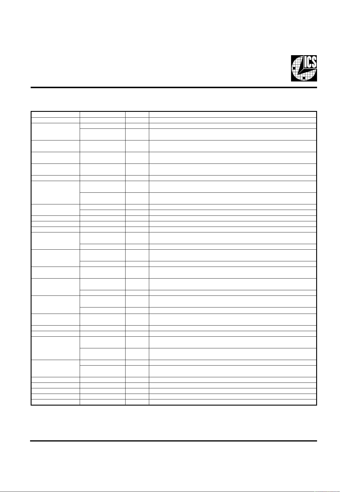
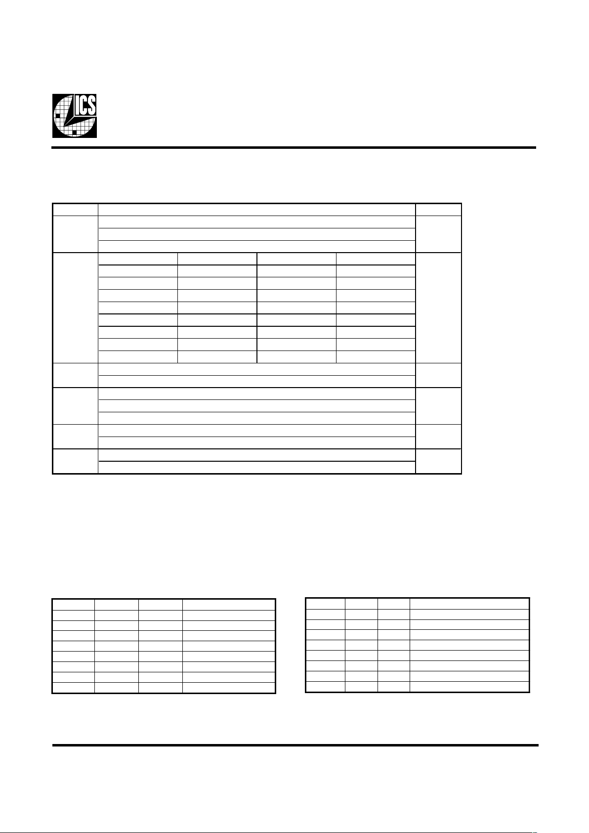
Block Diagram
9148-111 Rev A 10/19/99
Functionality
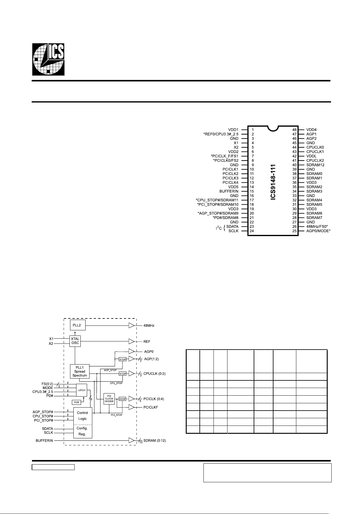
Pin Configuration
48-Pin 300mil SSOP
Recommended Application:
ALI (Aladdin V
) mobile.
Output Features:
• 3 - CPUs @ 2.5V/3.3V, up to 100MHz.
• 3 - AGPCLK @ 3.3V
• 13 - SDRAM @ 3.3V, up to 100MHz.
• 6 - PCI @ 3.3V, including one free running.
• 1 - 48MHz, @ 3.3V fixed.
• 1 - REF @ 3.3V, 14.318MHz.
Features:
• Up to 100MHz frequency support
• Support power management: CPU, PCI, AGP stop and,
Power down Mode from I
2
C programming.
• Spread spectrum for EMI control (0 to -0.6%, ± 0.25%).
• Uses external 14.318MHz crystal
• FS pins for frequency select
Key Specifications:
• CPU – CPU: <250ps
• SDRAM - SDRAM: <250ps
• AGP-AGP: <250ps
• PCI – PCI: <500ps
• CPU-SDRAM <500ps
• CPU(early)-PCI: 1-4ns, Center 2-6ns
• CPU-AGP <500ps
Frequency Generator & Integrated Buffers for PENTIUM/Pro
TM
* Internal Pull-up Resistor of
240K to 3.3V on indicated inputs
1 1 1 100 33.33 66.67 14.318
1 1 0 95.25 31.75 63.50 14.318
1 0 1 83.3 33.30 66.60 14.318
1 0 0 75 30.00 60.00 14.318
0 1 1 91.5 30.50 61.00 14.318
0 1 0 96.22 32.07 64.15 14.318
0 0 1 66.8 33.40 66.80 14.318
0 0 0 60 30.00 60.00 14.318
PCI
(MHz)
REF,
IOAPIC
(MHz)
FS2 FS1 FS0
CPU,
SDRAM
(MHz)
AGP
(MHz)
ICS reserves the right to make changes in the device data identified in
this publication without further notice. ICS advises its customers to
obtain the latest version of all device data to verify that any
information being relied upon by the customer is current and accurate.
Page 2
2
ICS9148-111
Third party brands and names are the property of their respective owners.
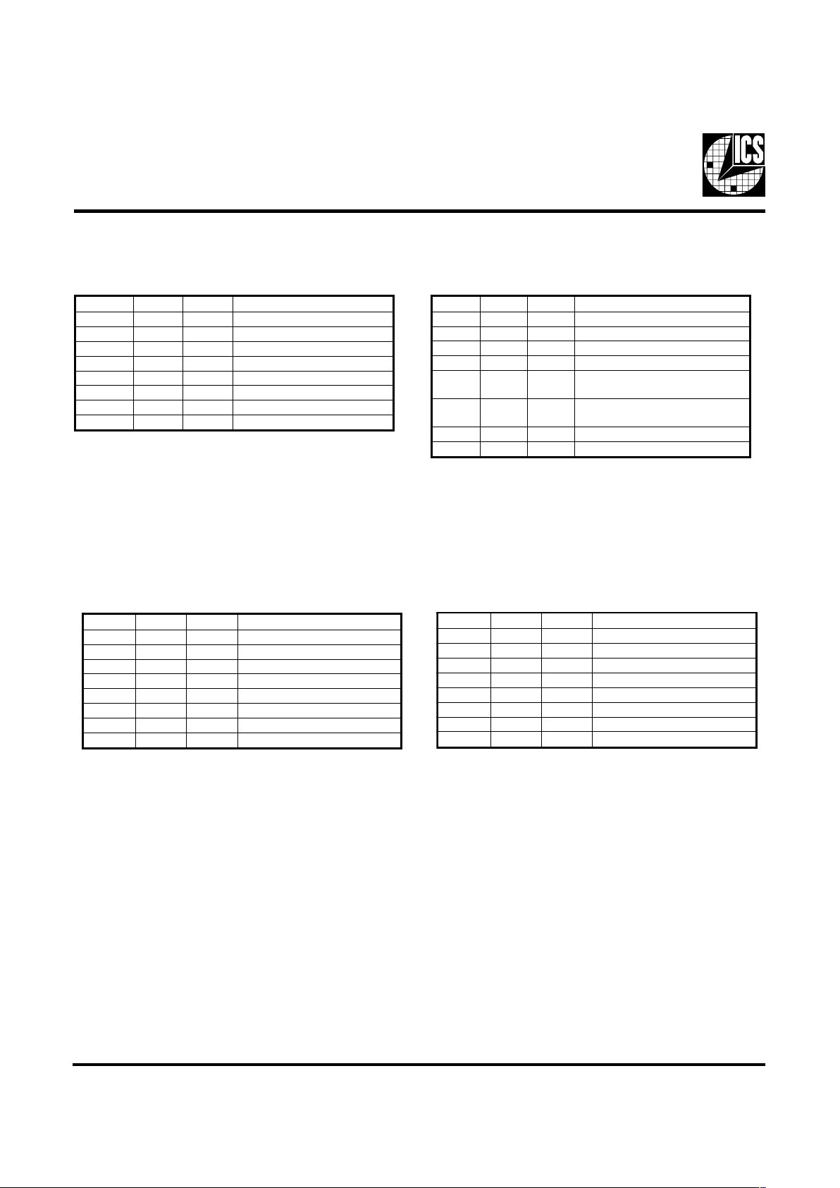
Pin Configuration
Notes:
1: Internal Pull-up Resistor of 240K to 3.3V on indicated inputs
2: Bidirectional input/output pins, input logic levels are latched at internal power-on-reset. Use 10Kohm resistor
to program logic Hi to VDD or GND for logic low.
REBMUNNIPEMANNIPEPYTNOITPIRCSED
11DDVRWPV3.3lanimon,ylppusrewopLATX,)2:0(feR
2
0FERTUO.kcolcecnereferzhM813.41
5.2_#3.3UPC
2,1
NI
V3.3=WOL,UPCV5.2=hgiH.V5.2roV3.3si2LDDVrehtehwsetacidnI
UPC
1
tupnidehctaL.
2
,72,22,61,9,3
54,93,33
DNGRWPdnuorG
41XNI
kcabdeefdna)Fp33(pacdaollanretnisah,tupnilatsyrC
2Xmorfrotsiser
52XTUO
daollanretnisaH.zHM813.41yllanimon,tuptuolatsyrC
)Fp33(pac
62DDVRWPV3.3lanimon,)5:0(KLCICPdnaF_KLCICProfylppuS
7
F_KLCICPTUO
wekssn4-1htiwsKLCUPChtiwsuonorhcnyS.tuptuokcolcICPgninnureerF
#POTS_ICPybdetceffatonsisihT)ylraeUPC(
1SF
2,1
NI
ehtsnimretedsnipSFrehtohtiwgnolA.tupnIdehctaL.niptcelesycneuqerF
.seicneuwerfPGA&ICP,MARDS,UPC
8
0KLCICPTUO )ylraeUPC(wekssn4-1htiwsKLCUPCsuonuorhcnyS.stuptuokcolcICP
2SF
2,1
NItupnIdehctaL.niptcelesycneuqerF
31,21,11,01)4:1(KLCICPTUO )ylraeUPC(wekssn4-1htiwsKLCUPCsuonuorhcnyS.stuptuokcolcICP
415DDVRWP0PGA,zHM84,LLPdexifrofylppuS
51NIREFFUBNI.sreffubMARDSrofniptupnI
71
#POTS_UPC
1
NI
eliboMni(woltupninehw,level0cigoltaskcolc)3:0(KLCUPCstlaH
)0=EDOM,edoM
11MARDSTUOtuptuokcolcMARDS
81
#POTS_ICP
1
NI
,edomelibomnI(woltupninehw,level0cigoltaskcolc)5:0(KLCICPstlaH
)0=EDOM
01MARDSTUOtuptuokcolcMARDS
,43,23,13,92,82
83,73,53
)9:0(MARDSTUO.stuptuokcolcMARDS
02
#POTS_PGANI
tupninehwlevel"0"cigoltaskcolc)2:1(PGAstlahtupnisuonorhcnysasihT
0PGAtceffatonseoD)0=EDOM,edoMeliboMni(wol
9MARDSTUOtuptuokcolcMARDS
12
#DPNI
lanretni&latsyrc,OCVehtspotStupninwoDrewoPsuonorehcnysasihT
)0=EDOM,edoMeliboMnI(.woL,evitcanehwskcolc
8MARDSTUOtuptuokcolcMARDS
63,03,913DDVRWP
,skcolczHM84,eroCUPC,)11:0(MARDSrofylppuS
.V3.3lanimon
32ATADSNIIroftupniataD
2
.tupnilairesC
42KLCSNIIfotupnikcolC
2
tupniC
52
0PGATUO
ybdetceffatoN.4DDVybderewop,tuptuotroPcihparGdecnavdA
#POTS_PGA
EDOM
2,1
NI
.edoMeliboM=0,edoMpotkseD=1,niptcelesnoitcnuf12&02,81,71niP
.tupnIdehctaL
62
zHM84TUO.gnimitBSUrofkcolctuptuozHM84
0SF
2,1
NI
ehtsnimretedsnipSFrehtohtiwgnolA.tupnIdehctaL.niptcelesycneuqerF
.seicneuwerfPGA&ICP,MARDS,UPC
44,34,14)3:0(KLCUPCTUOwoL=#POTS_UPCfiwoL.2LDDVybderewop,stuptuokcolcUPC
0421MARDSTUO.tuptuokcolcMARDSkcabdeeF
24LDDVRWPlanimonV3.3roV5.2rehtie,)3:0(UPCrofylppuS
74,64)2:1(PGATUO.4DDVybderewop,stuptuotroPcihparGdecnavdA
844DDVRWP)2:0(PGArofylppuS
Page 3
3
ICS9148-111
Third party brands and names are the property of their respective owners.
General Description Power Groups
VDD1 = REF (0:1), X1, X2
VDD2 = PCICLK_F, PCICLK(0:5)
VDD3 = SDRAM (0:12), supply for PLL core
VDD4 = AGP (1:2)
VDD5 = Fixed PLL, 48MHz , AGP0
VDDL = CPUCLK (0:2)
5.2_#3.3UPC
leveltupnI
)ataDdehctaL(
rofdetceleSreffuB
:tanoitarepo
1DDVV5.2
0DDVV3.3
CPU 3.3#_2.5V Buffer selector for CPUCLK drivers.
Power Management Functionality
Mode Pin - Power Management Input Control
52niP,EDOM
)tupnIdehctaL(
71niP81niP02niP12niP
0
#POTS_UPC
)TUPNI(
#POTS_ICP
)TUPNI(
#POTS_PGA
)TUPNI(
#DP
)TUPNI(
1
11MARDS
)TUPTUO(
01MARDS
)TUPTUO(
9MARDS
)TUPTUO(
8MARDS
)TUPTUO(
#POTS_PGA#POTS_UPC#POTS_ICP
,PGA
KLCUPC
stuptuO
KLCICP
)5:0(
,F_KLCICP
zHM84,FER
MARDSdna
latsyrC
CSO
OCV)2:1(PGA
101 woLdeppotSgninnuRgninnuRgninnuRgninnuRgninnuR
111 gninnuRgninnuRgninnuRgninnuRgninnuRgninnuR
110 gninnuRwoLdeppotSgninnuRgninnuRgninnuRgninnuR
011 gninnuRgninnuRgninnuRgninnuRgninnuRwoLdeppotS
The ICS9148-111 is a single chip clock solution for Desktop/
Notebook designs using the ALI (Aladdin V
) mobile style
chipset. It provides all necessary clock signals for such a
system.
Spread spectrum may be enabled through I2C programming.
Spread spectrum typically reduces system EMI by 8dB to
10dB. This simplifies EMI qualification without resorting to
board design iterations or costly shielding. The ICS9148-111
employs a proprietary closed loop design, which tightly
controls the percentage of spreading over process and
temperature variations.
Serial programming I2C interface allows changing functions,
stop clock programming and frequency selection.
Page 4
4
ICS9148-111
Third party brands and names are the property of their respective owners.
1. The ICS clock generator is a slave/receiver, I2C component. It can read back the data stored in the latches for
verification. Read-Back will support Intel PIIX4 "Block-Read" protocol.
2. The data transfer rate supported by this clock generator is 100K bits/sec or less (standard mode)
3. The input is operating at 3.3V logic levels.
4. The data byte format is 8 bit bytes.
5. To simplify the clock generator I
2
C interface, the protocol is set to use only "Block-Writes" from the controller. The
bytes must be accessed in sequential order from lowest to highest byte with the ability to stop after any complete byte
has been transferred. The Command code and Byte count shown above must be sent, but the data is ignored for those
two bytes. The data is loaded until a Stop sequence is issued.
6. At power-on, all registers are set to a default condition, as shown.
General I2C serial interface information
The information in this section assumes familiarity with I2C programming.
For more information, contact ICS for an I
2
C programming application note.
How to Write:
Controller (host) sends a start bit.
Controller (host) sends the write address D2
(H)
ICS clock will acknowledge
Controller (host) sends a dummy command code
ICS clock will acknowledge
Controller (host) sends a dummy byte count
ICS clock will acknowledge
Controller (host) starts sending first byte (Byte 0)
through byte 5
ICS clock will acknowledge each byte one at a time.
Controller (host) sends a Stop bit
How to Read:
Controller (host) will send start bit.
Controller (host) sends the read address D3
(H)
ICS clock will acknowledge
ICS clock will send the byte count
Controller (host) acknowledges
ICS clock sends first byte (Byte 0) through byte 5
Controller (host) will need to acknowledge each byte
Controller (host) will send a stop bit
Notes:
Controller (Host) ICS (Slave/Receiver)
Start Bit
Address
D3
(H)
AC
K
Byte Count
ACK
Byte
0
ACK
Byte 1
ACK
Byte
2
ACK
Byte
3
ACK
Byte 4
ACK
Byte
5
ACK
Stop Bit
How to Read:
Controller (Host) ICS (Slave/Receiver)
Start Bit
Address
D2
(H)
AC
K
Dummy Command Code
AC
K
Dummy Byte Count
AC
K
Byte 0
AC
K
Byte 1
ACK
Byte 2
AC
K
Byte 3
AC
K
Byte 4
AC
K
Byte 5
AC
K
Stop Bit
How to Write:
Page 5
5
ICS9148-111
Third party brands and names are the property of their respective owners.
Bit PWD
Bit6 Bit5 Bit4 CPU Clock PCI AGP
111
100 33.33 66.67
110
95.25 31.75 63.50
101
83.3 33.30 66.60
100
75 30.00 60.00
011
91.5 30.50 61.00
010
96.22 32.07 64.15
001
66.8 33.40 66.80
000
60 30.00 60.00
Description
Must be 0 for normal operation
0 - - +/ - 0.25% Spread S p e ctrum Modulation
1 -- +/- 0.6% Spread Spectrum Modulation
Bit 7
Bit 3
Bit 2
0
Note 1Bit 6:4
0 - R unning
0 - Fre quency is selected by har dware select, Latched i np uts
1 - Fre quency is selected by Bit 6:4 (above)
Must be 0 for normal operation
0 - Spre ad S pe c t rum ce nte r spread type.
Bit 1
Bit 0
1 - T ristate all out
p
uts
0
0
0
0
1 - Spre ad Spec t rum down spread type.
0 - Normal
1 - Spread Spectrum Enabled
Byte0: Functionality and Frequency Select Register (default = 0)
Serial Configuration Command Bitmap
Note 1. Default at Power-up will be for latched logic inputs to define frequency. Bits 4, 5, 6 are default to 000, and if
bit 3 is written to a 1 to use Bits 6:4, then these should be defined to desired frequency at same write cycle.
Note: PWD = Power-Up Default
Byte 1: CPU, Active/Inactive Register
(1 = enable, 0 = disable)
Notes:
1. Inactive means outputs are held LOW and are disabled
from switching.
Notes:
1. Inactive means outputs are held LOW and are disabled
from switching.
tiB#niPDWPnoitpircseD
7tiB-1 )devreseR(
6tiB-1 )devreseR(
5tiB-1 )devreseR(
4tiB041 )tcanI/tcA(21MARDS
3tiB-1 )devreseR(
2tiB141 )tcanI/tcA(2KLCUPC
1tiB341 )tcanI/tcA(1KLCUPC
0tiB441 )tcanI/tcA(0KLCUPC
tiB#niPDWPnoitpircseD
7tiB-1 )devreseR(
6tiB71 )tcanI/tcA(F_KLCICP
5tiB-1 )devreseR(
4tiB311 )tcanI/tcA(4KLCICP
3tiB211 )tcanI/tcA(3KLCICP
2tiB111 )tcanI/tcA(2KLCICP
1tiB011 )tcanI/tcA(1KLCICP
0tiB81 )tcanI/tcA(0KLCICP
Byte 2: PCI Active/Inactive Register
(1 = enable, 0 = disable)
Page 6
6
ICS9148-111
Third party brands and names are the property of their respective owners.
Byte 3: SDRAM Active/Inactive Register
(1 = enable, 0 = disable)
Notes:
1. Inactive means outputs are held LOW and are disabled
from switching.
tiB#niPDWPnoitpircseD
7tiB821 )tcanI/tcA(7MARDS
6tiB921 )tcanI/tcA(6MARDS
5tiB131 )tcanI/tcA(5MARDS
4tiB231 )tcanI/tcA(4MARDS
3tiB431 )tcanI/tcA(3MARDS
2tiB531 )tcanI/tcA(2MARDS
1tiB731 )tcanI/tcA(1MARDS
0tiB831 )tcanI/tcA(0MARDS
Byte 4: SDRAM Active/Inactive Register
(1 = enable, 0 = disable)
Byte 5: Peripheral Active/Inactive Register
(1 = enable, 0 = disable)
Notes:
1. Inactive means outputs are held LOW and are disabled
from switching.
Notes:
1. Inactive means outputs are held LOW and are disabled
from switching.
tiB#niPDWPnoitpircseD
7tiB521 )evitcanI/evitcA(0PGA
6tiB-1 )devreseR(
5tiB-1 )devreseR(
4tiB-1 )devreseR(
3tiB711
)tcanI/tcA(11MARDS
)ylnOedoMpotkseD(
2tiB811
)tcanI/tcA(01MARDS
)ylnOedoMpotkseD(
1tiB021 )tcanI/tcA(9MARDS
0tiB121 )tcanI/tcA(8MARDS
tiB#niPDWPnoitpircseD
7tiB-1 )devreseR(
6tiB-1 )devreseR(
5tiB-1 )devreseR(
4tiB741 )tcanI/tcA(1PGA
3tiB-1 )devreseR(
2tiB-1 )devreseR(
1tiB641 )tcanI/tcA(2PGA
0tiB21 )tcanI/tcA(0FER
Byte 6: Optional Register for Possible
Furture Requirements
Notes:
1. Byte 6 is reserved by Integrated Circuit Systems for
future applications.
tiB#niPDWPnoitpircseD
7tiB-1 )devreseR(
6tiB-1 )devreseR(
5tiB-1 )devreseR(
4tiB-1 )devreseR(
3tiB-1 )devreseR(
2tiB-1 )devreseR(
1tiB-1 )devreseR(
0tiB-1 )devreseR(
Page 7

7
ICS9148-111
Third party brands and names are the property of their respective owners.
Pins 2, 7, 8, 25 & 26 on the ICS9148-111 serve as dual signal
functions to the device. During initial power-up, they act as
input pins. The logic level (voltage) that is present on these
pins at this time is read and stored into a 4-bit internal data
latch. At the end of Power-On reset, (see AC characteristics
for timing values), the device changes the mode of operations
for these pins to an output function. In this mode the pins
produce the specified buffered clocks to external loads.
To program (load) the internal configuration register for these
pins, a resistor is connected to either the VDD (logic 1)
power supply or the GND (logic 0) voltage potential. A 10
Kilohm(10K) resistor is used to provide both the solid CMOS
programming voltage needed during the power-up
programming period and to provide an insignificant load on
the output clock during the subsequent operating period.
Figs. 1 and 2 show the recommended means of implementing
this function. In Fig. 1 either one of the resistors is loaded
onto the board (selective stuffing) to configure the devices
internal logic. Figs. 2a and b provide a single resistor loading
option where either solder spot tabs or a physical jumper
header may be used.
Shared Pin Operation Input/Output Pins
Fig. 1
These figures illustrate the optimal PCB physical layout
options. These configuration resistors are of such a large
ohmic value that they do not effect the low impedance clock
signals. The layouts have been optimized to provide as little
impedance transition to the clock signal as possible, as it
passes through the programming resistor pad(s).
Page 8

8
ICS9148-111
Third party brands and names are the property of their respective owners.
Fig. 2a
Fig. 2b
Page 9

9
ICS9148-111
Third party brands and names are the property of their respective owners.
AGP_STOP# Timing Diagram
Notes:
1. All timing is referenced to the internal CPUCLK.
2. AGP_STOP# is an asynchronous input and metastable conditions may exist.
This signal is synchronized to the CPUCLKs inside the ICS9148-111.
3. All other clocks continue to run undisturbed.
4. PD# and PCI_STOP# are shown in a high (true) state.
5. Only applies if MODE pin latched 0 at power up.
AGP_STOP# is an asychronous input to the clock synthesizer. It is used to turn off the AGP clocks. for low power operation.
AGP_STOP# is synchronized by the ICS9148-111. The AGPCLKs will always be stopped in a low state and start in such a
manner that guarantees the high pulse width is a full pulse. AGPCLK on latency is less than AGPCLK and AGPCLK off latency
is less than 4 AGPCLKs. This function is available only with MODE pin latched low.
Page 10

10
ICS9148-111
Third party brands and names are the property of their respective owners.
CPU_STOP# Timing Diagram
CPU_STOP# is an asychronous input to the clock synthesizer. It is used to turn off the CPU clocks for low power operation.
CPU_STOP# is synchronized by the ICS9148-111. The minimum that the CPU clock is enabled (CPU_STOP# high pulse) is 100
CPU clocks. All other clocks will continue to run while the CPU clocks are disabled. The CPU clocks will always be stopped in
a low state and start in such a manner that guarantees the high pulse width is a full pulse. CPU clock on latency is less than 4
CPU clocks and CPU clock off latency is less than 4 CPU clocks.
Notes:
1. All timing is referenced to the internal CPU clock.
2. CPU_STOP# is an asynchronous input and metastable conditions may exist. This signal is synchronized
to the CPU clocks inside the ICS9148-111.
3. All other clocks continue to run undisturbed. (including SDRAM outputs).
Page 11

11
ICS9148-111
Third party brands and names are the property of their respective owners.
PCI_STOP# Timing Diagram
PCI_STOP# is an asynchronous input to the ICS9148-111. It is used to turn off the PCICLK (0:5) clocks for low power
operation. PCI_STOP# is synchronized by the ICS9148-111 internally. The minimum that the PCICLK (0:5) clocks are enabled
(PCI_STOP# high pulse) is at least 10 PCICLK (0:5) clocks. PCICLK (0:5) clocks are stopped in a low state and started with a full
high pulse width guaranteed. PCICLK (0:5) clock on latency cycles are only one rising PCICLK clock off latency is one PCICLK
clock.
Notes:
1. All timing is referenced to the Internal CPUCLK (defined as inside the ICS9148 device.)
2. PCI_STOP# is an asynchronous input, and metastable conditions may exist. This signal is required to be synchronized
inside the ICS9148.
3. All other clocks continue to run undisturbed.
4. CPU_STOP# is shown in a high (true) state.
Page 12

12
ICS9148-111
Third party brands and names are the property of their respective owners.
PD# Timing Diagram
The power down selection is used to put the part into a very low power state without turning off the power to the part. PD# is
an asynchronous active low input. This signal needs to be synchronized internal to the device prior to powering down the clock
synthesizer.
Internal clocks are not running after the device is put in power down. When PD# is active low all clocks need to be driven to a
low value and held prior to turning off the VCOs and crystal. The power up latency needs to be less than 3 mS. The power down
latency should be as short as possible but conforming to the sequence requirements shown below. PCI_STOP# and
CPU_STOP# are considered to be don't cares during the power down operations. The REF and 48MHz clocks are expected to
be stopped in the LOW state as soon as possible. Due to the state of the internal logic, stopping and holding the REF clock
outputs in the LOW state may require more than one clock cycle to complete.
Notes:
1. All timing is referenced to the Internal CPUCLK (defined as inside the ICS9148-111 device).
2. As shown, the outputs Stop Low on the next falling edge after PD# goes low.
3. PD# is an asynchronous input and metastable conditions may exist. This signal is synchronized inside this part.
4. The shaded sections on the VCO and the Crystal signals indicate an active clock.
5. Diagrams shown with respect to 133MHz. Similar operation when CPU is 100MHz.
Page 13

13
ICS9148-111
Third party brands and names are the property of their respective owners.
Absolute Maximum Ratings
Supply Voltage . . . . . . . . . . . . . . . . . . . . . . . . . . . . 7.0 V
Logic Inputs . . . . . . . . . . . . . . . . . . . . . . . . . . . . . . GND 0.5 V to VDD +0.5 V
Ambient Operating Temperature . . . . . . . . . . . . . 0°C to +70°C
Storage Temperature . . . . . . . . . . . . . . . . . . . . . . . 65°C to +150°C
Stresses above those listed under Absolute Maximum Ratings may cause permanent damage to the device. These ratings are
stress specifications only and functional operation of the device at these or any other conditions above those listed in the
operational sections of the specifications is not implied. Exposure to absolute maximum rating conditions for extended periods
may affect product reliability.
Electrical Characteristics - Input/ Supply/Common Output Parameters
TA = 0 - 70º C; Supply Voltage VDD=3.3 V +\- 5%, V
DDL
= 2.5 V +/- 5% (unless otherwise stated)
PARAMETER SYMBOL CONDITIONS MIN TYP MAX UNITS
Input High V oltage
V
IH
2
V
DD
+0.3
V
Input Low Voltage
V
IL
VSS-0.3
0.8 V
Input High Current
I
IH
VIN = V
DD
0.1 5
µA
Input Low Current
I
IL1
VIN = 0 V; Input s with no pull-up resistors
-5 2.0
µA
Input Low Current
I
IL2
VIN = 0 V; Input s with pull-up resistors
-200 -100
µA
Operating
I
DD3.3OP66
Select @ 66.8MHz; CL=0; all outputs running 115 160 mA
Supply Current
I
DD3.3OP100
Select @ 100MHz; CL=0; all outputs running 140 190 mA
Power down Current
I
DD3.3PD
PD# = 0; Full capacitive loads
150 600
µA
Input fre quency
F
i
VDD = 3.3 V
12 14.318 16 MHz
In
p
ut Capacitance
1
C
IN
Logic Inpu ts 5 pF
C
INX
X1 & X2 pins 27 36 45 pF
Transition Time
1
T
Trans
To first crossing of target Freq. 0.65 2 ms
Settlin
g
Time
1
T
S
From first crossing to 1% of target Freq. 0.35 3 ms
Clk Stabilizatio n
1
T
STAB
From VDD = 3.3 V to 1% target Freq.
<1.5 2 ms
T
CPU-PCIVT
=1.5 V; f=66/100 MHz; VDD=V
DDL
22.54ns
Skew
1
T
CPU-PCIVT
=1.5 V; f=83/75 MHz; VDD=V
DDL
24.255 ns
T
AGP-PCIVT
= 1.5 V; AGP leads
400 700 ps
1
Guaranteed by design, not 100% tested i n production.
Electrical Characteristics - Input/Supply/Common Output Parameters
TA = 0 - 70º C; Supply Voltage VDD = 3.3 V +/-5%, V
DDL
= 2.5 V +/-5% (unless otherwise stated)
PARAMETER SYMBOL CONDITIONS MIN TYP MAX UNITS
Operating
I
DD2.5OP66
Select @ 66.8MHz; CL=0; all outputs running
15 30 mA
Supply Current
I
DD2.5OP100
Select @ 100MHz; CL=0; all outputs running
18 35 mA
1
Guaranteed by design, not 100% tested in production.
Page 14

14
ICS9148-111
Third party brands and names are the property of their respective owners.
Electrical Characteristics - CPU3.3
TA = 0 - 70º C; VDD = V
DDL
= 3.3 V +/-5%; CL = 20 pF (unless otherwise st ated)
PARAMETER SYMBOL CONDITIONS MIN TYP MAX UNITS
Output High Voltage
V
OH2B
IOH = -28 mA 2.5 2.6 V
Output Low Voltage
V
OL2B
IOL = 24 mA 0.34 0.4 V
Output High Current
I
OH2B
VOH =2.0 V -29 -23 mA
Output Low Current
I
OL2B
VOL = 0.8 V 33 52 mA
Rise Time t
r2B
1
VOL = 0.4 V, VOH = 2.4 V 1 2 ns
Fall Time t
f2B
1
VOH = 2.4 V, VOL = 0.4 V 0.9 2 ns
Duty Cycle d
t2B
1
VT = 1.5 V 45 52 55 %
Skew t
sk2B
1
VT = 1.5 V 90 175 ps
VT = 1.5 V; f=66/ 100 MHz 150 320 ps
VT = 1.5 V; f=75/83 MHz 285 550 ps
1
Guaranteed by design, not 100% tested in production.
2
Edge displacement of a period relative to a 10-clock-cycle rolling average period.
tj
srd2B
1
Jitter, Single Edge
Dis
p
lacement2
Electrical Characteristics - CPU2.5
TA = 0 - 70º C; VDD = 3.3 V +/-5%, V
DDL
= 2.5 V +/-5%; CL = 20 pF (unless otherwise st ated)
PARAMETER SYMBOL CONDITIONS MIN TYP MAX UNITS
Output High Voltage V
OH2B
IOH = -8.0 mA 2 2.2 V
Output Low Voltage V
OL2B
IOL = 12 mA 0.22 0.4 V
Output High Current I
OH2B
VOH =1.7 V -20 -16 mA
Output Low Current I
OL2B
VOL = 0.7 V 19 39 mA
Rise Time t
r2B
1
VOL = 0.4 V, VOH = 2.0 V 1 1.6 ns
Fall Time t
f2B
1
VOH = 2.0 V, VOL = 0.4 V 0.9 1.6 ns
Duty Cycle d
t2B
1
VT = 1.25 V 45 51 55 %
Skew t
sk2B
1
VT = 1.25 V 110 175 ps
Jitter, Single Edge tj
srd2B
1 VT = 1.25 V; f=66/1 00 MHz 170 340 ps
Displacement
2
VT = 1.25 V; f=75/83 MHz 310 680 ps
1
Guaranteed by design, not 100% tested in production.
2
Edge displacement of a period relative to a 10-clock-cycle rolling average period.
Page 15

15
ICS9148-111
Third party brands and names are the property of their respective owners.
Electrical Characteristics - PCICLK
TA = 0 - 70º C; VDD = 3.3 V +/-5%, V
DDL
= 2.5 V +/-5%; CL = 30 pF (unless otherwise st ated)
PARAMETER SYMBOL CONDITIONS MIN TYP MAX UNITS
Output High Volt age
V
OH1
IOH = -28 mA
2.4 3 V
Output Low Voltage
V
OL1
IOL = 23 mA
0.32 0.4 V
Output High Current
I
OH1
VOH = 2.0 V
-60 -40 mA
Output Low Current
I
OL1
VOL = 0.8 V
41 54 mA
Rise Time
1
t
r1
VOL = 0.4 V, VOH = 2.4 V
1.6 2 ns
Fall Time
1
t
f1
VOH = 2.4 V, VOL = 0.4 V
1.3 2 ns
Duty Cycle
1
d
t1
VT = 1.5 V
45 51 55 %
Skew
1
t
sk1
VT = 1.5 V
100 250 ps
Jitter, Single Edge
Dis
p
lacement2
tj
srd
1
V
T
= 1.5 V
220 500 ps
1
Guaranteed by design, not 100% tested in production.
2
Edge displacement of a period relative to a 10-clock-cycle rolling average period.
Electrical Characteristics - SDRAM
TA = 0 - 70º C; VDD = 3.3 V +/-5%, V
DDL
= 2.5 V +/-5%; CL = 30 pF (unless otherwise st ated)
PARAMETER SYMBOL CONDITIONS MIN TYP MAX UNITS
Output High Voltage V
OH3
IOH = -24 mA 2.4 2.9 V
Output Low Voltage V
OL3
IOL = 23 mA 0.35 0.4 V
Output High Current I
OH3
VOH = 2.0 V -68 -40 mA
Output Low Current I
OL3
VOL = 0.8 V 41 53 mA
Rise Time T
r3
1
VOL = 0.4 V, VOH = 2.4 V 1.4 2 ns
Fall Time T
f3
1
VOH = 2.4 V, VOL = 0.4 V 1.4 2 ns
Duty Cycle D
t3
1
VT = 1.5 V 48 54 60 %
V
T
= 1.5 V, Sdram 0,8,9,12 Window 140
V
T
= 1.5 V, Sdram 2,4,5,6 Window 120 250 ps
V
T
= 1.5 V, Sdram 1,3,7,10,11 Window 140
Propagation Delay
T
prop
VT = 1.5 V
3.5 4.5 ns
1
Guarenteed by design, not 100% tested in production.
Skew
1
T
sk1
Page 16

16
ICS9148-111
Third party brands and names are the property of their respective owners.
Electrical Characteristics - AGP
TA = 0 - 70º C; VDD = 3.3 V +/-5%, V
DDL
= 2.5 V +/-5%; CL = 30 pF (unless otherwise stated)
PARAMETER SYMBOL CONDITIONS MIN TYP MAX UNITS
Output High Volt age V
OH1
IOH = -28 mA 2.4 3 V
Output Low Voltage V
OL1
IOL = 23 mA 0.32 0.4 V
Output High Current I
OH1
VOH = 2.0 V -60 -40 mA
Output Low Current I
OL1
VOL = 0.8 V 41 54 mA
Rise Time
1
t
r1
VOL = 0.4 V, VOH = 2.4 V 1.3 2 ns
Fall Time
1
t
f1
VOH = 2.4 V, VOL = 0.4 V 1.2 2 ns
V
T
= 1.5 V, AGP0 45 51 55 %
V
T
= 1.5 V, AGP1:2 48 53 58 %
Skew
1
t
sk1
VT = 1.5 V 110 250 ps
Jitter, Single Edge V
T
= 1.5 V, AGP0 660 1200 ps
Displacement
2
VT = 1.5 V, AGP1:2
310 650 ps
1
Guaranteed by design, not 100% tested in production.
2
Edge displacement of a period relative to a 10-clock-cycle rolling average period.
Duty Cycle
1
d
t1
tj
srd
1
Electrical Characteristics - REF0, 48MHz
TA = 0 - 70º C; VDD = 3.3 V +/-5%, V
DDL
= 2.5 V +/-5%; CL = 20 pF (unless otherwise stated)
PARAMETER SYMBOL CONDITIONS MIN TYP MAX UNITS
Output High Voltage V
OH5
IOH = -16 mA 2.4 2.6 V
Output Low Voltage V
OL5
IOL = 9 mA 0.24 0.4 V
Output High Current I
OH5
VOH = 2.0 V -32 -22 mA
Output Low Current I
OL5
VOL = 0.8 V 16 28 mA
Rise Time
1
t
r5
VOL = 0.4 V, VOH = 2.4 V 1.5 4 ns
Fall Time
1
t
f5
VOH = 2.4 V, VOL = 0.4 V 2.1 4 ns
Duty Cycle
1
d
t5
VT = 1.5 V, REF0 50 55 60 %
V
T
= 1.5 V, 48M 46 5 5 56 %
Jitter, Single Edge tj
srd5
VT = 1.5 V, REF0 430 750 ps
Displacement
2
VT = 1.5 V, 48M 790 1200 ps
V
T
= 1.5 V, REF0 -550 350 550 ps
V
T
= 1.5 V, 48M
-700 520 700 ps
1
Guaranteed by design, not 100% tested in production.
2
Edge displacement of a period relative to a 10-clock-cycle rolling average period.
Jitter, Absolute
1
t
jabs5
Page 17

17
ICS9148-111
Third party brands and names are the property of their respective owners.
= Routed Power
= Ground Connection Key (component side copper)
= Ground Plane Connection
= Power Route Connection
= Solder Pads
= Clock Load
C3
1
Clock Load
2
C1
C1
48
47
46
45
44
43
42
41
40
39
38
37
36
35
34
33
32
31
30
29
28
27
26
25
1
2
3
4
5
6
7
8
Ferrite
Bead
VDD
C2
22µF/20V
Tantalum
Ferrite
Bead
VDD
C2
22µF/20V
Tantalum
1
2
3
4
5
6
7
8
9
10
11
12
13
14
15
16
17
18
19
20
21
22
23
24
Ground
2.5V Power Route
3.3V Power Route
3.3V Power Route
Connections to VDD:
General Layout Precautions:
1) Use a ground plane on the top routing
layer of the PCB in all areas not used
by traces.
2) Make all power traces and ground
traces as wide as the via pad for lower
inductance.
Notes:
1 All clock outputs should have
provisions for a 15pf capacitor
between the clock output and series
terminating resistor. Not shown in all
places to improve readability of
diagram.
2 Optional crystal load capacitors are
recommended. They should be
included in the layout but not
inserted unless needed.
Component Values:
C1 : Crystal load values determined by user
C2 : 22µF/20V/D case/Tantalum
AVX TAJD226M020R
C3 : 15pF capacitor
FB = Fair-Rite products 2512066017X1
All unmarked capacitors are 0.01µF ceramic
Page 18

18
ICS9148-111
Third party brands and names are the property of their respective owners.
SSOP Package
LOBMYS SNOISNEMIDNOMMOC SNOITAIRAV D N
.NIM.MON.XAM.NIM.MON.XAM
A590.101.011.CA026.526.036.84
1A800.210.610.
2A880.090.290.
B800.010.5310.
C500.- 010.
DsnoitairaVeeS
E292.692.992.
eCSB520.0
H004.604.014.
h010.310.610.
L420.230.040.
NsnoitairaVeeS
µ
°0 °5 °8
X580.390.001.
Ordering Information
ICS9148yF-111
Pattern Number (2 or 3 digit number for parts with ROM code patterns)
Package Type
F=SSOP
Revision Designator (will not correlate with datasheet revision)
Device Type (consists of 3 or 4 digit numbers)
Prefix
ICS, AV = Standard Device
Example:
ICS XXXX y F - PPP
ICS reserves the right to make changes in the device data identified in
this publication without further notice. ICS advises its customers to
obtain the latest version of all device data to verify that any
information being relied upon by the customer is current and accurate.
 Loading...