

Page 1
Integrated
Circuit
Systems, Inc.
General Description Features
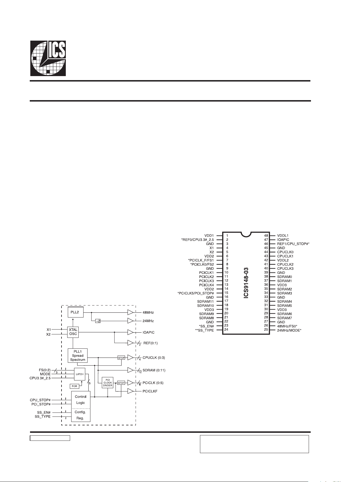
ICS9148-03
Block Diagram
Pentium is a trademark of Intel Corporation
Frequency Generator & Integrated Buffers for PENTIUM/Pro
TM
9148-03 Rev A 091997P
Pin Configuration
48-Pin SSOP
Power Groups
VDD1 = REF (0:1), XTAL, 24MHz, 48MHz
VDD2 = PCICLK_F, PCICLK(0:5)
VDD3 = SDRAM (0:11), supply for PLL core,
24MHz, 48MHz
VDDL1 = IOAPIC
VDDL2 = CPU (0:3)
* Internal Pull-up Resistor of
240K to 3.3V on indicated inputs
** Internal Pulldown to GND
3.3V outputs: SDRAM, PCI, REF, 48/24MHz.
2.5V or 3.3V outputs: CPU, IOAPIC
20 ohm CPU clock output impedance
20 ohm PCI clock output impedance
Skew from CPU (earlier) to PCI clock - 1 to 4 ns,
center 2.6 ns.
No external load cap for CL=18pF crystal
±250 ps CPU, PCI clock skew
400ps (cycle to cycle) CPU jitter
2ms power up clock stable time.
Clock duty cycle 45-55%.
48 pin 300 mil SSOP package
3.3V operation, 5V tolerant input.
The ICS9148-03 generates all clocks required for high
speed RISC or CISC microprocessor systems such as Intel
PentiumPro or Cyrix. Eight different reference frequency
multiplying factors are externally selectable with smooth
frequency transitions.
Features include four CPU, seven PCI and Twelve SDRAM
clocks. Two reference outputs are available equal to the
crystal frequency. Plus the IOAPIC output powered by
VDDL1. One 48 MHz for USB, and one 24 MHz clock for
Super IO. Spread Spectrum built in - ±1.5% modulation to
reduce the EMI. Rise time adjustment for VDD at 3.3V or
2.5V CPU. Additionally, the device meets the Pentium
power-up stabilization, which requires that CPU and PCI
clocks be stable within 2ms after power-up. It is not
recommended to use I/O dual function pin for the slots
(ISA, PCI, CPU, DIMM). The add on card might have a pull up
or pull down.
High drive PCICLK and SDRAM outputs typically provide
greater than 1 V/ns slew rate into 30pF loads. CPUCLK
outputs typically provide better than 1V/ns slew rate into
20pF loads while maintaining 50±5% duty cycle. The REF
and 24 and 48 MHz clock outputs typically provide better
than 0.5V/ns slew rates.
ADVANCE INFORMATION documents contain information on
new products in the sampling or preproduction phase of development. Characteristic data and other specifications are subject to
change without notice.
Page 2
2
ICS9148-03
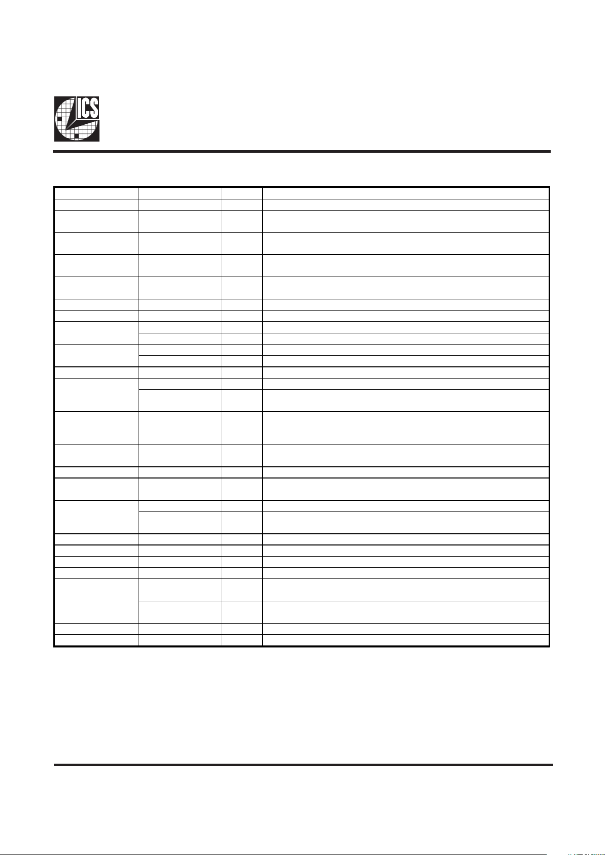
Pin Descriptions
Notes:
1: Internal Pull-up Resistor of 240K to 3.3V on indicated inputs
2: Bidirectional input/output pins, input logic levels are latched at internal power-on-reset. Use 10Kohm resistor
to program logic high to VDD logic low to GND.
3. Internal Pulldown Resistor of 240K to GND on SS_type
PIN NUMBER PIN NAME TYPE DESCRIPTION
1 VDD1 PWR Ref (0:1), XTAL power supply, nominal 3.3V
2
REF0 OUT 14.318 MHz ref erence clock.
CPU3.3#_2.5
1,2
IN
Indicates whether VDDL2 is 3.3V or 2.5V. High=2.5V CPU, LOW=3.3V
CPU. Latched Input.
3,9,16,22,27,
33,39,45
GND PWR Ground
4X1 IN
Crystal input, has internal load cap (33pF) and feedback
resistor from X2
5 X2 OUT Cryst al output, nominally 14.318MHz. Has internal load cap (33pF)
6,14 VDD2 PWR Supply for PCICLK_F and PCICLK (0:5), nominal 3.3V
7
PCICLK_F OU T Free r unning PCI cloc k
FS1
1,2
IN Frequency sel ect pin. Latche d Input.
8
PCICLK0 OU T PCI clock output.
FS2
1,2
IN Frequency sel ect pin. Latche d Input.
10, 11, 12, 13 PCICLK(1:4) OU T PCI clock outputs.
15
PCICLK5 O UT PCI clock output. (In desktop mode, MODE= 1)
PCI_STOP#
1
IN
Halts PCICLK (0:5) clocks at logic 0 level, when input low
(In mobile mode, MODE=0)
17, 18, 20, 21,
28, 29, 31, 32,
34, 35,37,38
SDRAM (0:11) OU T SDRAM clock outputs.
19,30,36 VDD3 PW R
Supply for SDRA M (0:11), PLL core and 24, 48M Hz clocks, nomi nal
3.3.V
23 SS_EN#
1
IN Spread Spectrum En able. Low =Enabl e
24 SS_TYPE
3
IN
HIGH = Spread Spectrum down spread. LOW = Spread S pectrum Center
spread. Input has Pulldown to GND
25
24MHz OU T 24M Hz output clock
MODE
1,2
IN
Pin 15, pin 46 funct ion select pin, 1 =Desktop Mode, 0= Mobile mode.
Latched Input .
26 48MHz OU T 48 MHz output cloc k
FS0
1,2
IN Frequency sel ect pin. Latche d Input.
40, 41, 43, 44 CPUCLK(0:3) O UT CPU clock outputs, powered by VDDL2. Low if CP U_STOP#=Low
42 VDDL2 PW R Supply for CPU (0:3), ei ther 2.5V or 3.3V nominal
46
REF1 OUT
14.318 Mhz refere nce clock.(in Deskto p Mode, MODE=1) This R EF Output
is the STRONGER buffer for ISA loads.
CPU_STOP#
1
IN
Halts CPUCLK (0:3) clocks at logic 0 level when input low
(in Mobile Mode, M ODE=0)
47 IOAPIC OUT IOAPIC clock output. 14.318 MHz Powered by VDDL1.
48 VD DL 1 PW R Supply for IOAPIC , either 2.5V or 3.3V nomi nal
Page 3
3
ICS9148-03
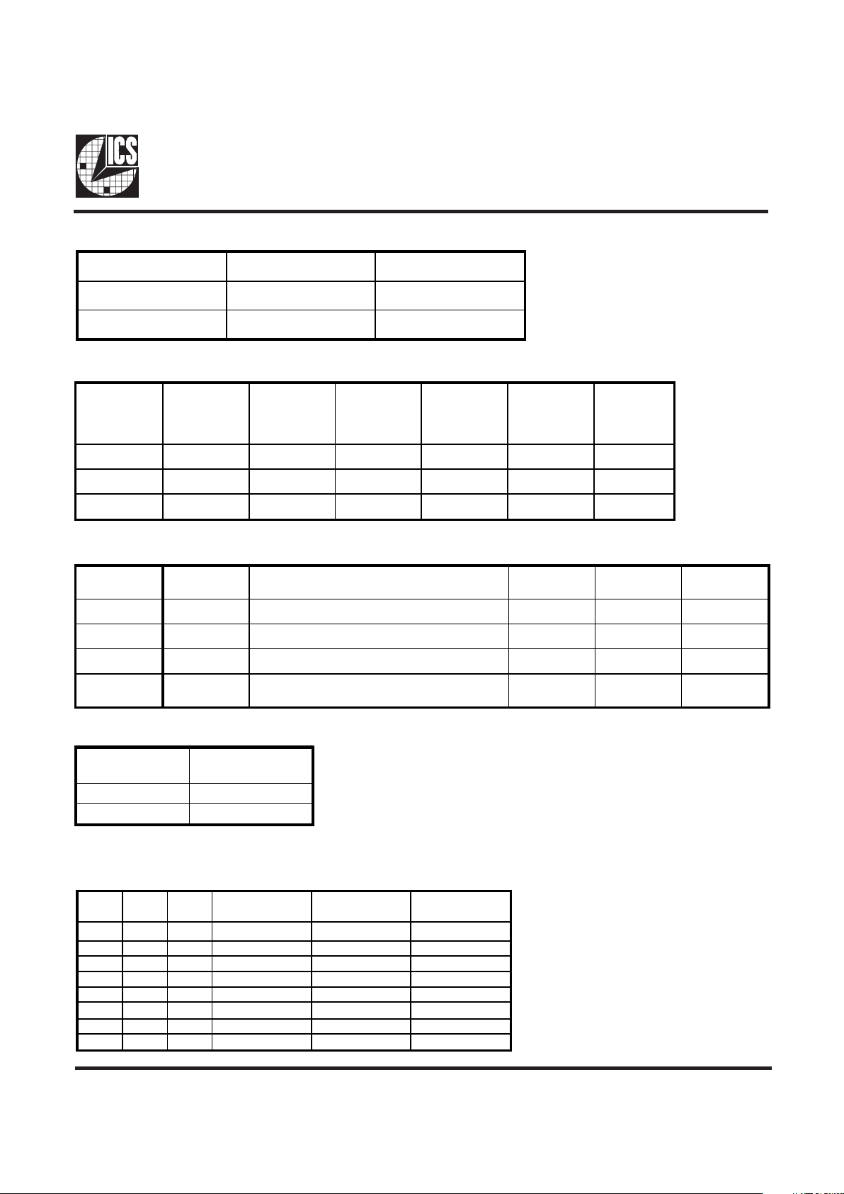
Mode Pin - Power Management Input Control
Power Management Functionality
Spread Spectrum Functionality
CPU3.3#_2.5
Input level
Buffer Selected for
operation at:
12.5V VDD
03.3V VDD
CPU 3.3#_2.5V Buffer selector for CPUCLK and IOAPIC drivers.
FS2 FS1 FS0
CPU,
SDRAM(MHz)
PCICLK
(MHz)
REF, IOAPIC
(MHz)
0 0 0 50.0 25.0 (1/2 CPU) 14.318
0 0 1 75.0 32 14.318
0 1 0 83.3 41.65 (1/2 CPU) 14.318
0 1 1 68.5 34.25 (1/2 CPU) 14.318
1 0 0 83.3 33.3 14.318
1 0 1 75.0 37.5 (1/2 CPU) 14.318
1 1 0 60.0 30.0 (1/2 CPU) 14.318
1 1 1 66.8 33.4 (1/2 CPU) 14.318
Functionality
VDD1,2,3 = 3.3V±5%, V
DDL
1,2 = 2.5V±5% or 3.3±5%, TA= 0 to 70°C
Crystal (X1, X2) = 14.31818MHz
Pin 23
SSEN#
Pin 24
SS_Type
CPU, SDRAM
and PCICLOCKS
REF, IOAPIC 24MHz 48MHz
0 0 Frequency Modulated Center Spread Mode 14.318MHz 24MHz 48MHz
0 1 Frequency Modulated Down Spread Mode 14.318MHz 24MHz 48MHz
1 0 Normal, Steady Frequency Mode 14.318MHz 24MHz 48MHz
11
Not Allowed
(will lower average frequency)
14.318MHz 24MHz 48MHz
MODE, Pin 25
(Latched Input)
Pin 46 Pin 15
0
CPU_STOP#
(INPUT)
PCI_STOP#
(INPUT)
1
REF1
(OUTPUT)
PCICLK5
(OUTPUT)
CPU_STOP# PCI_STOP#
CPUCLK
Outputs
PCICLK
(0:5)
PCICLK_F,
REF,
24/48MHz
and SDRAM
Crystal
OSC
VCO
0 1 Stopp ed Low Running Running Running R unning
1 1 Running Running Running Running Running
1 0 Running Stopped Low Running Running Running
Page 4
4
ICS9148-03
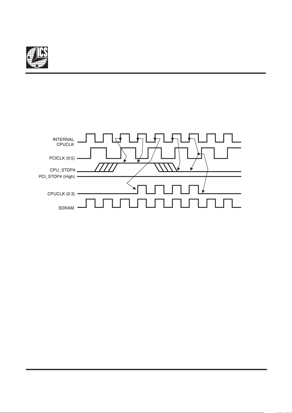
CPU_STOP# Timing Diagram
CPU_STOP# is an asychronous input to the clock synthesizer. It is used to turn off the CPU clocks for low power
operation. CPU_STOP# is synchronized by the ICS9148-03. The minimum that the CPU clock is enabled (CPU_STOP#
high pulse) is 100 CPU clocks. All other clocks will continue to run while the CPU clocks are disabled. The CPU clocks
will always be stopped in a low state and start in such a manner that guarantees the high pulse width is a full pulse. CPU
clock on latency is less than 4 CPU clocks and CPU clock off latency is less than 4 CPU clocks.
Notes:
1. All timing is referenced to the internal CPU clock.
2. CPU_STOP# is an asynchronous input and metastable conditions may exist. This signal
is synchronized to the CPU clocks inside the ICS9148-03.
3. All other clocks continue to run undisturbed.
Page 5

5
ICS9148-03
Notes:
1. All timing is referenced to the Internal CPUCLK (defined as inside the ICS9148 device.)
2. PCI_STOP# is an asynchronous input, and metastable conditions may exist. This signal is required to be synchronized
inside the ICS9148.
3. All other clocks continue to run undisturbed.
4. CPU_STOP# is shown in a high (true) state.
PCI_STOP# Timing Diagram
PCI_STOP# is an asynchronous input to the ICS9148-03. It is used to turn off the PCICLK (0:5) clocks for low power
operation. PCI_STOP# is synchronized by the ICS9148-03 internally. The minimum that the PCICLK (0:5) clocks are
enabled (PCI_STOP# high pulse) is at least 10 PCICLK (0:5) clocks. PCICLK (0:5) clocks are stopped in a low state and
started with a full high pulse width guaranteed. PCICLK (0:5) clock on latency cycles are only one rising PCICLK clock
off latency is one PCICLK clock.
Page 6

6
ICS9148-03
Pins 2, 7, 8, 25 and 26 on the ICS9148-03 serve as dual signal
functions to the device. During initial power-up, they act as
input pins. The logic level (voltage) that is present on these
pins at this time is read and stored into a 4-bit internal data
latch. At the end of Power-On reset, (see AC characteristics
for timing values), the device changes the mode of operations
for these pins to an output function. In this mode the pins
produce the specified buffered clocks to external loads.
To program (load) the internal configuration register for
these pins, a resistor is connected to either the VDD (logic
1) power supply or the GND (logic 0) voltage potential. A
10 Kilohm(10K) resistor is used to provide both the solid
CMOS programming voltage needed during the power-up
programming period and to provide an insignificant load
on the output clock during the subsequent operating
period.
Figs. 1 and 2 show the recommended means of
implementing this function. In Fig. 1 either one of the
resistors is loaded onto the board (selective stuffing) to
configure the devices internal logic. Figs. 2a and b provide
a single resistor loading option where either solder spot tabs
Shared Pin Operation Input/Output Pins
Fig. 1
or a physical jumper header may be used.
These figures illustrate the optimal PCB physical layout
options. These configuration resistors are of such a large
ohmic value that they do not effect the low impedance
clock signals. The layouts have been optimized to provide
as little impedance transition to the clock signal as possible,
as it passes through the programming resistor pad(s).
Page 7

7
ICS9148-03
Fig. 2a
Fig. 2b
Page 8

8
ICS9148-03
Absolute Maximum Ratings
Supply Voltage . . . . . . . . . . . . . . . . . . . . . . . . . . . 7.0 V
Logic Inputs . . . . . . . . . . . . . . . . . . . . . . . . . . . . GND 0.5 V to VDD +0.5 V
Ambient Operating Temperature . . . . . . . . . . . . 0°C to +70°C
Storage Temperature . . . . . . . . . . . . . . . . . . . . . . 65°C to +150°C
Stresses above those listed under Absolute Maximum Ratings may cause permanent damage to the device. These ratings are
stress specifications only and functional operation of the device at these or any other conditions above those listed in the
operational sections of the specifications is not implied. Exposure to absolute maximum rating conditions for extended periods
may affect product reliability.
Elect rical C haracteri sti cs - I np ut /S upp ly/ C om mon O ut pu t P aram et ers
TA = 0 - 70C; Supply Voltage VDD = V
DDL
= 3.3 V +/-5% (unless otherwise stated)
PARAMETER SYMBOL CONDITIONS MIN TYP MAX UNITS
Input H igh Voltage V
IH
2V
DD
+0.3 V
Input Low Voltage V
IL
VSS-0.3 0.8 V
Input H igh Curr ent I
IH
VIN = V
DD
0.1 5 µA
Input Low Cur r e nt I
IL1
VIN = 0 V; Inputs wi th no pul l- up resistors -5 2 µA
Input Low Cur r e nt I
IL2
VIN = 0 V; Inputs wi th pul l- up resistors -200 -1 00 µA
Operati ng I
DD3.3OPCL
= 0 pF; Select @ 66MHz 100 160 mA
Supply Current
Input F r e quenc y F
i
VDD = 3.3 V 12 14.318 16 MHz
Input Capac i tanc e
1
C
IN
L ogic I nputs 5 pF
C
INX
X1 & X2 pins 27 36 45 ps
Tr ansi tion T ime
1
T
trans
To 1st crossing of target Fr eq. 2 ms
Clk Stabilization
1
T
STAB
From VDD = 3.3 V to 1% target Freq. 2 ms
Skew
1
t
CPU-SDRAM1
VT = 1.5 V 500 ps
t
CPU-PCI1VT
= 1.5 V
12.6 4 ns
1
Guar antee d by design, not 100% tested in producti on.
Electrical Characteristics - Input/S upply/Com mon O utput Parameters
TA = 0 - 70C; Supply V oltage VDD = 3.3 V +/-5%, V
DDL
= 2.5 V +/-5 % ( unless otherwi se stated)
PARAMETER SYMBOL CONDITIONS MIN TYP MAX UNITS
Oper ating S upply Curr ent I
DD2.5OP
CL = 0 pF; Select @ 66.8 MHz 8 20 m A
Skew
1
t
CPU-SDRAM2VT
= 1.5 V; VTL = 1.25 V 800 ps
t
CPU-PCI2
VT = 1.5 V; VTL = 1.25 V
14ps
1
G uaranteed by design, not 100% tested in production.
Page 9

9
ICS9148-03
Ele ctri cal Characteri sti c s - CPU
TA = 0 - 70C; VDD = 3.3 V +/-5%, V
DDL
= 2.5 V +/-5%; CL = 20 pF
PARAMETER SYMBOL CONDITIONS MIN TY P MAX UNITS
O utput Impedance
1
R
DSP2B
VO = VDD*(0.5) 13.5 45 Ohm
O utput Impedance
1
R
DSN2B
VO = VDD*(0.5) 13.5 45 Ohm
O utput High Volta ge V
OH2BIOH
= -8 mA 2 2.2 V
Output Low Voltage V
OL2BIOL
= 12 mA 0.3 0.4 V
Ou tput Hig h Current I
OH2B
VOH = 1.7 V -20 -16 mA
Output Low Current I
OL2B
VOL = 0.7 V 19 26 mA
Rise Time
1
t
r2B
VOL = 0.4 V, VOH = 2.0 V 2.2 2.5 ns
Fall Time
1
t
f2B
VOH = 2.0 V , VOL = 0.4 V 1.1 1.6 ns
Duty Cycle
1
d
t2B
VT = 1.25 V 45 55 %
Skew
1
t
sk2B
VT = 1.25 V 250 ps
Jitter, Cyc le-to-cycle
1
t
jcyc-cyc2BVT
= 1.25 V 200 400 ps
Jitter , O ne Sigma
1
t
j1s2B
VT = 1.25 V 50 150 ps
Jitter, Absolute
1
t
jabs2B
VT = 1.25 V
-300 300 ps
1
Guarante e d by de sign, not 100% tested in production.
Ele ctri cal Characteri sti c s - PCI
TA = 0 - 70C; VDD = V
DDL
= 3.3 V +/-5%; CL = 30 pF
PARAMETER SY MBOL CONDITIONS MIN TYP MAX UNITS
O utput Impedance
1
R
DSP1
VO = VDD*(0.5) 10 24 Ohm
O utput Impedance
1
R
DSN1
VO = VDD*(0.5) 10 24 Ohm
O utput High Volta ge V
OH1
IOH = -28 mA 2.4 3 V
Output Low Voltage V
OL1
IOL = 23 mA 0.2 0.4 V
Ou tput Hig h Current I
OH1
VOH = 2.0 V -60 -40 mA
Output Low Current I
OL1
VOL = 0.8 V 41 50 mA
Rise Time
1
t
r1
VOL = 0.4 V, VOH = 2.4 V 1.6 2 ns
Fall Time
1
t
f1
VOH = 2.4 V , VOL = 0.4 V 1.2 2 ns
Duty Cycle
1
d
t1
VT = 1.5 V 45 51 55 %
Skew
1
t
sk1
VT = 1.5 V 100 250 ps
Jitter , O ne Sigma
1
t
j1s1
VT = 1.5 V, synchronous 1 00 300 ps
t
j1s1a
VT = 1.5 V, a synchronous 2 00 400 ps
Jitter, Absolute
1
t
jabs1
VT = 1.5 V, synchronous -500 500 ps
t
jabs1a
VT = 1.5 V, a synchronous
-1000 1000 ps
1
Guarante e d by de sign, not 100% tested in pr odu c tion.
Page 10

10
ICS9148-03
Ele ctrical C haracterist ics - SDRA M
TA = 0 - 70C; VDD = V
DDL
= 3.3 V +/-5%; CL = 30 pF
PARAMETER SY MBOL CONDITIONS MIN TYP MAX UNITS
O utput Impedance
1
R
DSP1
VO = VDD*(0.5) 10 24
Ω
O utput Impedance
1
R
DSN1
VO = VDD*(0.5) 10 24
Ω
O utput Hi gh Volt ag e V
OH1
IOH = -28 mA 2.4 3 V
Output Low Voltage V
OL1
IOL = 23 mA 0.2 0.4 V
Ou t put Hi g h Current I
OH1
VOH = 2.0 V -60 -40 mA
Output Low Current I
OL1
VOL = 0.8 V 41 50 mA
Rise Time
1
T
r1
VOL = 0.4 V, VOH = 2.4 V 1.6 2 ns
Fall Time
1
T
f1
VOH = 2.4 V , VOL = 0.4 V 1.2 2 ns
Duty Cycle
1
D
t1
VT = 1.5 V 45 52 55 %
Skew
1
T
sk1
VT = 1.5 V 150 250 ps
Jitter, One Sigma
1
T
j1s1
VT = 1.5 V 50 150 ps
Jitter, Absol ute
1
T
jabs1
VT = 1.5 V
-250 +250 ps
1
Guarante e d by de sign, not 10 0% tested in produ c t ion.
Electrical Characteristics - IOAPIC
TA = 0 - 70C; VDD = 3.3 V +/-5%, V
DDL
= 2.5 V +/-5%; CL = 20 pF
PARAMETER SYMBOL CONDITIONS MIN TYP MAX UNITS
O utput Impedance
1
R
DSP4B
VO = VDD*(0.5) 13.5 45 Ohm
O utput Impedance
1
R
DSN4B
VO = VDD*(0.5) 13.5 45 Ohm
O utput Hi gh Volta ge V
OH4BIOH
= -8 mA 2 2.2 V
Output Low Voltage V
OL4BIOL
= 12 mA 0.3 0.4 V
Ou tput Hig h Current I
OH4B
VOH = 1.7 V -20 -16 mA
Output L ow Current I
OL4B
VOL = 0.7 V 19 26 mA
Rise Time
1
T
r4B
VOL = 0.4 V, VOH = 2.0 V 1.4 1.7 ns
Fall Time
1
T
f4B
VOH = 2.0 V , VOL = 0.4 V 1.3 1.6 ns
Duty Cycle
1
D
t4B
VT = 1.25 V 50 60 %
Jitter, O ne S igm a
1
T
j1s4B
VT = 1.25 V 1 3 %
Jitter, Absol ute
1
T
jabs4B
VT = 1.25 V
-5 5 %
1
Guaranteed by design, not 100% tested in produ c t ion.
Page 11

11
ICS9148-03
Electrical C haracterist ics - 24,48 MH z, REF(0:1)
TA = 0 - 70C; VDD = V
DDL
= 3.3 V +/-5%; CL = 10 - 20 pF (unless otherwise stated)
PARAMETER SY MBOL CONDITIONS MIN TYP MAX UNITS
O utpu t Frequency F
O48m
48 PPM
O utpu t Frequency F
OREF
14.318 MHz
O utput Impedance
1
R
DSP5
VO = VDD*(0.5) 20 60 Ohm
O utput Impedance
1
R
DSN5
VO = VDD*(0.5) 20 60 Ohm
O utput Hi gh Volt ag e V
OH5
IOH = -16 mA 2.4 2.6 V
Output Low Voltage V
OL5
IOL = 9 mA 0.3 0.4 V
Ou tput Hi gh Curr ent I
OH5
VOH = 2.0 V -32 -22 mA
Output Low Current I
OL5
VOL = 0.8 V 16 25 mA
Rise Time
1
t
r5
VOL = 0.4 V, VOH = 2.4 V 1.7 4 ns
Fall Time
1
t
f5
VOH = 2.4 V , VOL = 0.4 V 1.6 4 ns
Duty Cycle
1
d
t5
VT = 1.5 V 45 53 55 %
Jitter, One Si gma
1
t
j1s5
VT = 1.5 V 1 3 %
Jitter, Absol ute
1
t
jabs5
VT = 1.5 V
38%
1
Guarante e d by de sign, not 10 0% tested in production.
Page 12

12
ICS9148-03
SSOP Package
Ordering Information
ICS9148F-03
Pattern Number (2 or 3 digit number for parts with ROM code patterns)
Package Type
F=SSOP
Device Type (consists of 3 or 4 digit numbers)
Prefix
ICS, AV = Standard Device
Example:
ICS XXXX F - PPP
SYMBOL C OMMON DIMENSIONS VARIATIONS D N
MIN. NOM . M AX. MIN. NOM. MAX.
A .095 .101 .110 AC .620 .625 .630 48
A1 .008 .012 .016
A2 .088 .090 .092
B .008 .010 .0135
C.005- .010
D See Variati ons
E . 292 .296 .299
e0.025 BSC
H .400 .406 .410
h .010 .013 .016
L .024 .032 .040
N See Variati ons
∝
0° 5° 8°
X .085 .093 .100
ADVANCE INFORMATION documents contain information on
new products in the sampling or preproduction phase of development. Characteristic data and other specifications are subject to
change without notice.
 Loading...