

Page 1
Integrated
Circuit
Systems, Inc.
General Description Features
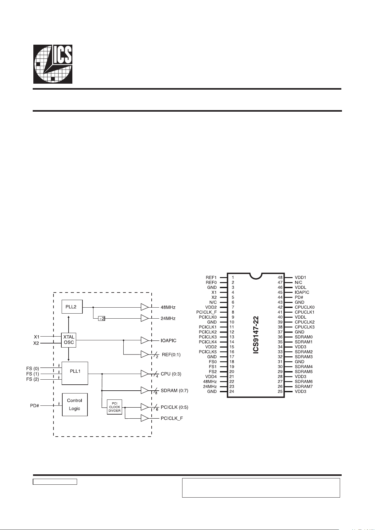
ICS9147-22
Block Diagram
Pentium/ProTM System and Cyrix Clock Chip
9147-22 Rev A 072597P
Pin Configuration
48-Pin SSOP
Pentium is a trademark on Intel Corporation.
Generates system clocks for CPU, IOAPIC, SDRAM,
PCI, plus 14.318 MHz (REF0:1), USB, Super I/O
Supports single or dual processor systems
Supports Intel 60, 66.8MHz, Cyrix 55, 75MHz plus 83.3
and 68MHz (Turbo of 66.6) speeds.
Synchronous clocks skew matched to 250ps window on
CPU, SDRAM and 500ps window on PCI clocks
CPU clocks to PCI clocks skew 1-4ns (CPU early)
Two fixed outputs, 48MHz and 24 MHz
Separate 2.5V and 3.3V supply pins
- 2.5V or 3.3V output: CPU, IOAPIC
- 3.3V outputs: SDRAM, PCI, REF, 48/24 MHz
No power supply sequence requirements
48 pin 300 mil SSOP
The ICS9147-22 is a Clock Synthesizer chip for Pentium
and PentiumPro plus Cyrix CPU based Desktop/Notebook
systems that will provide all necessary clock timing.
Features include four CPU, seven PCI and eight SDRAM
clocks. Two reference outputs are available equal to the
crystal frequency, plus the IOAPIC output powered by
VDDL. Additionally, the device meets the Pentium powerup stabilization, which requires that CPU and PCI clocks
be stable within 2ms after power-up.
High drive PCICLK and SDRAM outputs typically provide
greater than 1 V/ns slew rate into 30pF loads. CPUCLK
outputs typically provide better than 1V/ns slew rate into
20pF loads while maintaining 50 ±5% duty cycle. The REF
clock outputs typically provide better than 0.5V/ns slew
rates.
The ICS9147-22 accepts a 14.318MHz reference crystal
or clock as its input and runs on a 3.3V supply.
Power Groups
VDD1 = REF (0:1), X1, X2
VDD2 = PCICLK_F, PCICLK (0:5)
VDD3 = SDRAM (0:7),
VDD4 = 48MHz, 24MHz
VDDL = IOAPIC, CPUCLK (0:3)
ICS reserves the right to make changes in the device data identified in this
publication without further notice. ICS advises its customers to obtain the latest
version of all device data to verify that any information being relied upon by the
customer is current and accurate.
Page 2
2
ICS9147-22
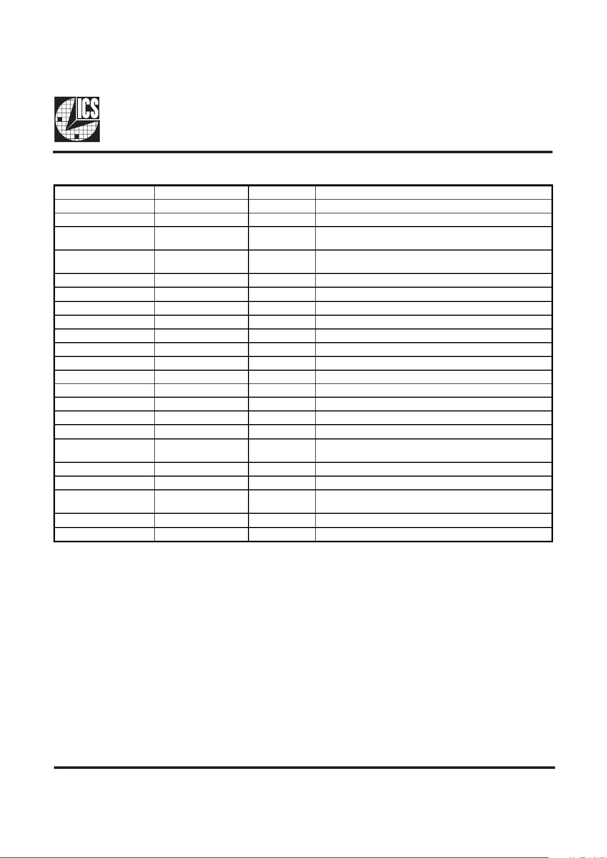
Pin Descriptions
PIN NUMBER PIN NAME TYPE DESCRIPTION
1 REF1 OUT Reference clock output
2 REF0 OUT Reference clock output
3, 10, 17, 24, 31,
31, 37, 43
GND PWR Ground (common)
4X1 IN
Crystal or refer ence input, no minally 14.3 18 MHz. Includes
internal load cap to GND an d feedback resistor from X2.
5 X2 OUT Crystal output, includes internal load cap to GND.
6, 47 N/C - Pins are not internally connected
7, 15 VDD2 PWR Supply for PCICLKF, and PCICLK (0:5)
8 PCICLK_F OUT Free running PCI clock
9, 11, 12, 13, 14, 16 PCICLK (0:5) OUT PCI clocks
18 FS0 IN Frequency sele ct 0 input
1
19 FS1 IN Frequency sele ct 1 input
1
20 FS2 IN Frequency sele ct 2 input
1
21 VDD4 PWR Supply for 48MHz and 24MHz clocks
22 48MHz OUT 48MHz driver output for USB clock
23 24MHz OUT 24MHz driver output for Super I/O clock
25, 28,34 VDD3 PWR Supply for SDRAM (0:7)
26, 27, 29, 30,
32, 33, 35, 36
SDRAM (0:7) OUT SDRAMs clock at CPU speed
38, 39, 41, 42 CPUCLK (0:3) OUT CPUCLK clock output, powered by VDDL
40, 46 VDDL PWR Supply for CPUCLK (0:3) + IOAPIC
44 PD# IN
Power down stops all clocks low and disab les oscillator and
internal VCO’s.
2
45 IOAPIC OUT IOAPIC clock output, powe red by VDDL at crystal frequency
48 VDD1 PWR Supply for REF (0:1), X1, X2
Note 1: Internal pull-up resistor of nomimally 100K to 120K at 3.3V on indicated inputs.
Note 2: The PD# input pin has a protection diode clamp to the VDDL power supply. If VDDL is not connected to VDD, (ie
VDDL=2.5V, VDD=3.3V) then this input must have a series resistor if the logic high is connected to VDD. This input
series resistor provides current limit for the clamp diode. For a pullup to VDD it should be 1Kohm or more from the PD#
pin to VDD. If the PD# pin is being driven by logic powered by 3.3V, then a 100Ω series resistor will be suffcient.
Page 3
3
ICS9147-22
Functionality
VDD = 3.3V ±5% V
DDL
= 2.5V ±5% or 3.3V ±5%, TA = 0 to 70°
Crystal (X1, X2) = 14.31818 MHz
Power Management Functionality
FS2 FS1 FS0
CPUCLK, SDRAM
(MHz)
PCICLK
(MHz)
0 0 0 8.33 1/2 CPU
0 0 1 75 30
0 1 0 83.3 33.3
0 1 1 68.5 1/2 CPU
1 0 0 55 1/2 CPU
1 0 1 75 1/2 CPU
1 1 0 60 1/2 CPU
1 1 1 66.8 1/2 CPU
PD#
CPUCLK
Outputs
PCICLK(0:5)
Outputs
PCICLK_ F,
REF,
24/48MHz
and SDRAM
Crystal
OSC
VCO
0 Stopped Low Stopped Low Stopped Low Off Off
1 Running Running Running Running Running
Page 4

4
ICS9147-22
Technical Pin Function Descriptions
VDD(1,2,3,4)
This is the power supply to the internal core logic of the
device as well as the clock output buffers for REF(0:1),
PCICLK, 48/24MHz and SDRAM(0:7).
This supply operates at 3.3 volts. Clocks from the listed
buffers that it supplies will have a voltage swing from Ground
to this level. For the actual guaranteed high and low voltage
levels for the Clocks, please consult the DC parameter table
in this data sheet.
VDDL
This is the power supply for the CPUCLK and IOAPIC output
buffers. The voltage level for these outputs may be 2.5 or 3.3
volts. Clocks from the buffers that each supplies will have a
voltage swing from Ground to this level. For the actual
guaranteed high and low voltage levels of these Clocks,
please consult the DC parameter table in this Data Sheet.
GND
This is the power supply ground (common or negative)
return pin for the internal core logic and all the output
buffers.
X1
This input pin serves one of two functions. When the
device is used with a Crystal, X1 acts as the input pin for
the reference signal that comes from the discrete crystal.
When the device is driven by an external clock signal, X1
is the device input pin for that reference clock. This pin
also implements an internal Crystal loading capacitor that
is connected to ground. See the data tables for the value
of this capacitor. Also includes feedback resistor from X2.
X2
This Output pin is used only when the device uses a
Crystal as the reference frequency source. In this mode of
operation, X2 is an output signal that drives (or excites)
the discrete Crystal. The X2 pin will also implement an
internal Crystal loading capacitor that is connected to
ground. See the Data Sheet for the value of this capacitor.
CPUCLK (0:3)
These Output pins are the Clock Outputs that drive
processor and other CPU related circuitry that requires
clocks which are in tight skew tolerance with the CPU
clock. The voltage swing of these Clocks is controlled by the
Voltage level applied to the VDDL2 pin of the device. See the
Functionality Table for a list of the specific frequencies that
are available for these Clocks and the selection codes to
produce them.
SDRAM(0:7)
These Output Clocks are use to drive Dynamic RAMs and
are low skew copies of the CPU Clocks. The voltage swing of
the SDRAMs output is controlled by the supply voltage
that is applied to VDD3 of the device, operating at 3.3 volts.
48MHz
This is a fixed frequency Clock output at 48MHz that is
typically used to drive USB devices.
24MHz
This pin is a fixed frequency clock output typically used
to drive Super I/O devices.
IOAPIC
This Output is a fixed frequency Output Clock that runs at
the Reference Input (typically 14.31818MHz) . Its voltage
level swing is controlled by VDDL and may operate at 2.5
or 3.3volts.
REF(0:1)
The REF Outputs are fixed frequency Clocks that run at
the same frequency as the Input Reference Clock X1 or the
Crystal (typically 14.31818MHz) attached across X1 and
X2.
PCICLK_F
This Output is equivalent to PCICLK(0:5) and is FREE
RUNNING.
PCICLK (0:5)
These Output Clocks generate all the PCI timing
requirements for a Pentium/Pro based system. They
conform to the current PCI specification. They run at 1/2
CPU frequency, or CPU/2.5; see frequency table.
FS0,1,2
These Input pins control the frequency of the Clocks at the
CPU, PCICLK and SDRAM output pins. See frequency
table.
PD#
This input pin stops all clocks in the low state and powers
down the oscillator and VCOs.
Page 5

5
ICS9147-22
Absolute Maximum Ratings
Electrical Characteristics at 3.3V
Supply Voltage . . . . . . . . . . . . . . . . . . . . . . . . . . . 7.0 V
Logic Inputs . . . . . . . . . . . . . . . . . . . . . . . . . . . . GND 0.5 V to VDD +0.5 V
Ambient Operating Temperature . . . . . . . . . . . . 0°C to +70°C
Storage Temperature . . . . . . . . . . . . . . . . . . . . . . 65°C to +150°C
VDD = 3.0 3.7 V, TA = 0 70° C unless otherwise stated
Note 1: Parameter is guaranteed by design and characterization. Not 100% tested in production.
Stresses above those listed under Absolute Maximum Ratings may cause permanent damage to the device. These ratings are
stress specifications only and functional operation of the device at these or any other conditions above those listed in the
operational sections of the specifications is not implied. Exposure to absolute maximum rating conditions for extended periods
may affect product reliability.
DC Characteristics
PARAMETER SYMBOL TEST CONDITIONS MIN TYP MAX UNITS
Input Low Voltage VIL Latched inputs and Fulltime inputs - - 0.2VDD V
Input High Voltage VIH Latched inputs and Fu lltime inputs 0.7V DD - - V
Input Low Current IIL VIN = 0V (Fulltime inputs) -28.0 -10.5 - µA
Input High Current IIH VIN=VDD (Fulltime inputs) -5.0 - 5.0 µA
Output Low Current
IOL1a
VOL = 0.8V; CPU, SDRAM, 48MHz;
VDDL = 3.3V
19.0 30.0 - mA
IOL1b VOL = 0.8V; CPU; VDDL = 2.5V 19.0 30.0 mA
Output High C urrent
IOH1a
VOH = 2.0V; CPU, SDRAM, 48MHz;
VDDL = 3.3V
--26.0-16.0 mA
IOH1b VOH = 2.0V; CPU; VDDL = 2.5V -12.5 -9.5 m A
Output Low Current
IOL2a
VOL = 0.8V; 24, PCI, REF, IOAPIC;
VDDL = 3.3V
16.0 25.0 - mA
IOL2b
VOL = 0.8V; IOAPIC;
VDDL = 2.5V
16.0 25.0 mA
Output High C urrent
IOH2a
VOH = 2.0V for REF, PCI, 24MHz &
IOAPIC at VDDL = 3.3V
--40.0-14.0mA
IOH2b VOH = 2.0V; IOAPIC; VDDL = 2.5V -13.0 -4.0 mA
Output Low Voltage
VOL1a
IOL = 10mA; CPU, SDRAM, 48MHz;
VDDL = 3.3V
-0.30.4V
VOL1b IOL = 10mA; CPU; VDDL=2.5V 0.3 0.4 V
Output High Voltage
VOH1a
IOH = -10mA; CPU, SDRAM, 48MHz;
VDDL = 3.3V
2.4 2.8 - V
VOH1b IOH = -10mA; CPU; VDDL=2.5V 1.95 2.1 V
Output Low Voltage
VOL2a
IOL = 10mA; for R EF, PCI, 24M Hz &
IOAPIC at VDDL = 3.3V
-0.30.4V
VOL2b
IOL = 10mA; IO APIC;
VDDL = 2.5V
0.3 0.4 V
Output High Voltage
VOH2a
IOH = -10mA; for REF, PCI, 24MHz &
IOAPIC at VDDL = 3.3V
2.4 2.8 - V
VOH2b IOH = -10mA; IOAPIC; VDDL = 2.5V 1.6 2.1 - V
Supply Current IDD @66.6 MHz; all outputs unload ed - 120 180 mA
Supply Current IDDPD Power Down 300 500 µ A
Page 6

6
ICS9147-22
Electrical Characteristics at 3.3V
VDD = 3.0 3.7 V, TA = 0 70° C unless otherwise stated
Note 1: Parameter is guaranteed by design and characterization. Not 100% tested in production.
Note 2: Includes VDDL = 2.5V
Note 3: VDD3 = 3.3V
AC Characteristics
PARAMETER SYMBOL TEST CONDITIONS MIN TYP MAX UNITS
Rise Time
1
Tr1a
20pF load, 0. 8 to 2.0V
CPU, 48MHz; VDD = 3.3V
-0.91.5ns
Rise Time
1
Tr1b
20pF load, 0. 8 to 2.0V
CPU; VDDL @ 2.5V
-1.52.0ns
Fall Time
1,3
Tf1 20pF load, 2.0 to 0.8V CPU, 48MHz; - 0.8 1.4 ns
Rise Time
1
Tr2 30pF load SDRAM 0.8 to 2.0V - 1.0 1.6 ns
Fall Time
1
Tf2 30pF load SDRAM 2.0 to 0.8V - 0.9 1.5 ns
Rise Time
1
Tr3 30pF load PCI 0.8 to 2.0V - 1.2 2.0 ns
Fall Time
1
Tf3 30pF load P CI 2.0 to 0.8V - 1.1 1. 9 ns
Rise Time
1,3
Tr4
20pF load, 0. 8 to 2.0V
24MHz, REF1 & IOAPIC
- 0.83 1.4 ns
Rise Time
1
Tr4a
20pF load, 0. 8 to 2.0V , IOAPI C with
VDDL = 2.5V
-2.22.6 ns
Fall Time
1,3
Tf4
20pF load, 2. 0 to 0.8V
24MHz, REF1 & IOAPIC
- 0.81 1.3 ns
Rise Time
1
Tr5
Load = 45pF 0.8 to 2.0V REF0
VDD = 3.3V
1.6 2.0 ns
Fall Time
1
Tf5
Load = 45pF 2.0 t o 0.8V, REF0
VDD = 3.3V
1.6 2.0 ns
Duty Cycle
1
Dt 20pF load @ VOUT=1.4 V 45 50 55 %
Jitter, Cycle to Cycle
1
Tjc-c CPU, VDDL = 3.0 to 3.7V 200 300 ps
Jitter, One Sigma
1
Tj1s1
CPU; Load=20pF,
SDRAM Load = 30pF
- 50 150 ps
Jitter, Absolute
1,
Tjab1
CPU; Load=20pF,
SDRAM Load = 30pF
-250 - 250 ps
Jitter, One Sigma
1
Tj1s1a CPU; Load=20pF VDDL=2.5V - 100 200 ps
Jitter, Absolute
1
Tjab1a CPU; Load=20pF VDDL=2.5V -500 - 500 ps
Jitter, One Sigma
1
Tj1s2 PCI; Load=30pF - 80 150 ps
Jitter, Absolute
1
Tjab2 PCI; Load=30pF -500 - 500 ps
Jitter, One Sigma
1
Tj1s3
REF1, 48/2 4MHz Load= 20pF,
REF0 CL = 45pF
- 1 3 %
Jitter, Absolute
1
Tjab3
REF1, 48/2 4MHz Load= 20pF,
REF0 CL = 45pF
-5 2 5 %
Input Frequency
1
Fi 12.0 14.318 16.0 MHz
Logic Input Capacitance
1
CIN Logic input pins - 5 - pF
Crystal Oscillator Capacitance
1
CINX X1, X2 pins - 18 - pF
Power-on Time
1
ton
From VDD=1.6V to 1st crossing of
66.6 MHz VDD supply ramp < 40ms
-2.54.5 ms
Clock Skew
1
Tsk1
CPU to CPU; Load=20pF; @1.4V
(Same VDD)
- 150 250 ps
Clock Skew
1
Tsk2
SDRAM to SDRAM;
Load=30pF @ 1.4V
- 150 250 ps
Clock Skew
1
Tsk3 PC I to PCI; Lo ad=30pF; @1 .4V - 300 500 ps
Clock Skew
1,2
Tsk4
CPU(20pF) to PCI (30pF); @1.4V
(CPU is early)
1 2.6 4 ns
Clock Skew
1
Tsk4
SDRAM (30pF @3.3V) to CPU
(20pF @2.5V) (2.5V CPU is late)
250 400 ps
Page 7

7
ICS9147-22
Ordering Information
ICS9147F-22
Pattern Number (2 or 3 digit number for parts with ROM code patterns)
Package Type
F=SSOP
Device Type (consists of 3 or 4 digit numbers)
Prefix
ICS, AV = Standard Device
Example:
ICS XXXX F - PPP
SSOP Package
SYMBOL CO MMON DIMENSIONS VARIATIONS D N
MIN. NOM. MAX. MIN. NOM. MAX.
A .095 .101 .110 AC .620 .625 .630 48
A1 .008 .012 .016 AD .720 .725 .730 56
A2 .088 .090 .092
B . 008 .010 .0135
C . 005 .006 .0085
D See Variations
E .292 .296 .299
e0.025 BSC
H .400 .406 .410
h .010 .013 .016
L .024 .032 .040
N See Variations
∝
0° 5° 8°
X .085 .093 .100
This table in inches
ICS reserves the right to make changes in the device data identified in this
publication without further notice. ICS advises its customers to obtain the latest
version of all device data to verify that any information being relied upon by the
customer is current and accurate.
 Loading...