

Page 1
9134-06 9134-07 RevC111695
Integrated
Circuit
Systems, Inc.
ICS913 4-0 6
ICS913 4-0 7
Advanc e Informa tion
32 kHz Motherboard Frequency Generator
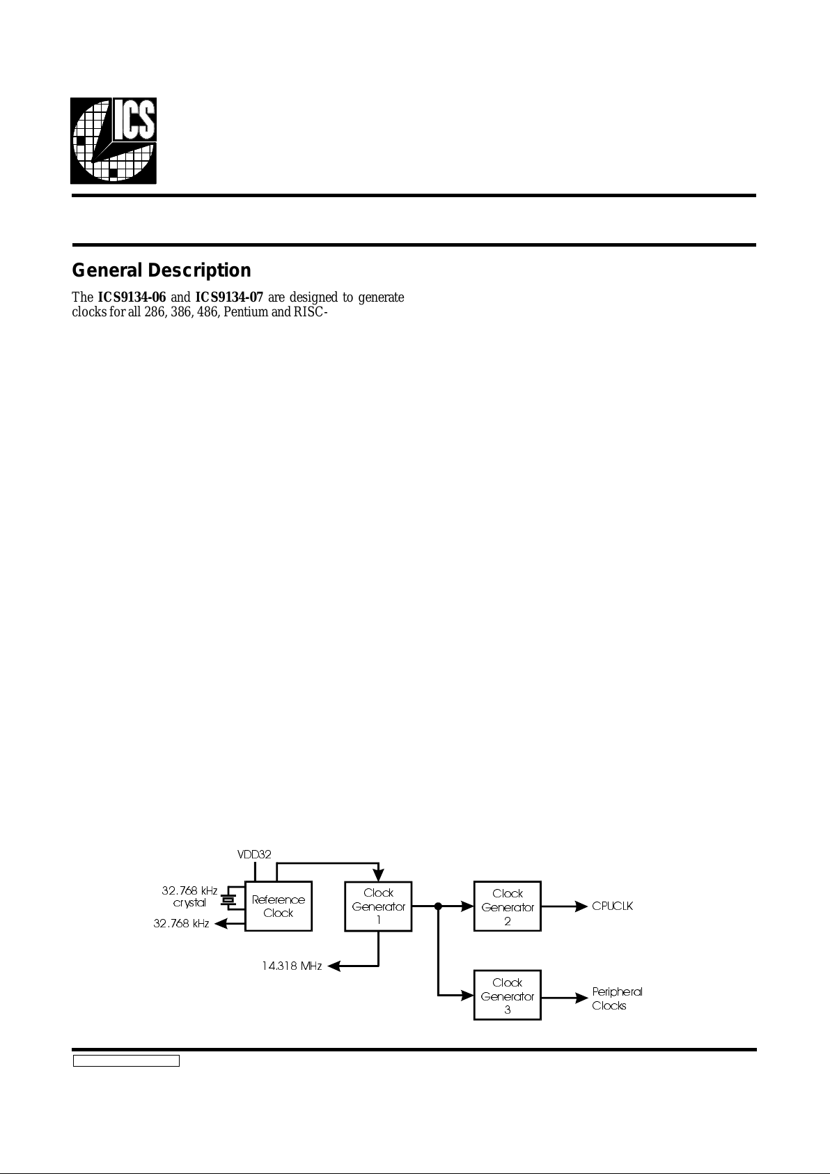
Block Diagram
VDD32
14.318 MHz
Peripheral
Clocks
CPUCLK
32.768 kHz
32.768 kHz
crystal
Reference
Clock
Clock
Generator
1
Clock
Generator
2
Clock
Generator
3
General Description
The ICS9134-06 and ICS9134-07 are designed to generate
clocks for al l 286, 386, 486, Penti um and RISC- based m other boards, including laptops and notebook computers. The only
external components required are a 32.768 kHz crystal and
decoupling capacitors. The device generates the 14.318 MHz
system clock, eliminating the need for a 14.318 MHz crystal.
High performance applications may require high speed clock
termi na ti on c om pone nt s. T he chip incl ude s three independent
clock generators plus the 32.768 kHz reference clock to produce all necessary frequencies, including real time
clock/DRAM refresh, master clock, CPU clock, keyboard
clock, floppy disk controller clock, serial communications
clock and bus c locks. Diff erent fre quencies fr om clocks # 2 can
be selected using the frequency select pins, but clock #1 will
be at 14.318 MHz for all standard versions.
VDD32 Supply
The ICS9134-06 an d ICS9 134-07 have a separate power su pply for the 32.768 kHz oscillator circuitry. This allows the
32 kHz clock to run from a battery or other source while the
main power to the chip is disconnected. The VDD32 supply is
guaranteed to operate down to +2.0V, with the clock consuming
less tha n 1 0µA at +3.3V with the main VD D at 0 V.
The frequencies and power-down options in the ICS9134-06
and ICS9134-07 are mask programmable. Customer specific
masks can b e made and p rototy pes de livere d wit hin 6- 8 week s
from receipt of order. Integrated Circuit Systems also offers
standard ver sions, such as that desc ri bed in this da ta sheet .
Applications
Notebook/Palmtop Computers: The ICS9134-06 and
ICS9134-07 work with +3.3V and +5V and a single
32.768 kHz crystal, making i t the ide al solut ion for gener atin g
clocks in portables with minimum board space. The user can
save power by using this single part instead of oscillators or
other frequ ency gene rator s. T he ICS9134-06 and ICS9134-07
further reduce the current consumption by having the ability to
completely shut down the individual clocks when not in use, while
still maintaining the separately powe red 32.768 kHz cloc k.
Features
•• IDD <10 µA when 32 kHz is running on VDD32
•• Single 32.768 kHz crystal generates all PC motherboard
cloc ks
•• 3 independent cloc k ge nerator s
•• Generates CPU clocks from 4.0 to 80 MHz
•• Up to 5 output clocks
•• Separate VDD for 32 kHz clock
•• Power-down opt io ns ava ila bl e
•• Operates from 3.3V or 5. 0V supp ly
•• Operate s up to 66 MHz at 3.3V
•• Supports OPTi 80C463 /5 and Fir chipsets
•• 16-pin, 300-mil, SOIC package
Fir is a trademark of Picopower Corporation.
Page 2
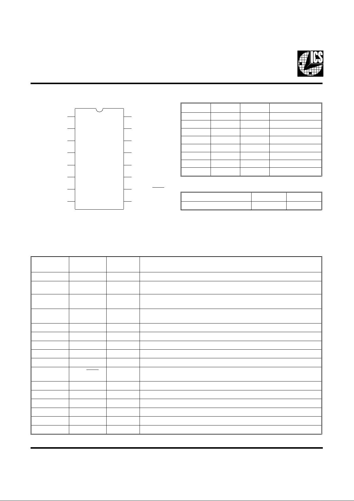
Pin Configuration
Pin Descriptions
PIN
NUMBER
PIN
NAME TYPE
DESCRIPTION
1
CPUS2
I
Select 2 for 2XCPU and CPU frequencies. See Table above.
2
X2
O Crystal conne ction. Connect to 32. 768 kHz crystal. Includes intern al
XTAL load capacitance.
3
X1
I
Crystal conne cti on. Conn ect to 32.76 8 kHz crysta l. This pi n i nc lud es
interna l XTAL load ca pa ci ta nc e an d fe ed ba ck bia s for a 32. 768 kHz crystal.
4
VDD32
P
Separate power supply c onnection for 32.768 kHz cl ock. Will operate down to
2.0V, independent of the rest of the circuit VDD.
5
VDD
P
Connect to +3.3V or +5V.
6
GND
P
Connect to ground.
7
24M
O
24 MHz floppy (or sup er I/O) clo ck outp ut.
8
32K
O
32.768 kHz square wave cloc k out put .
9
KBOUT
O
Keyboard clock outp ut, fixe d 16 MHz (-06) or 12 MHz (-07).
10
PD24+KBD
I
Power-down 24M+keyboard. Shuts off both clock outputs, pins 7 & 9 when
low.
11
14.3M
O
14.318 MHz system clock output.
12
GND
P
Connect to ground.
13
VDD
P
Connect to +3.3V or +5V.
14
CPUCLK
O
CPUCLK output . See Table above.
15
CPUS0
I
Select 0 for 2XCPU and CPU frequencies. See Table above.
16
CPUS1
I
Select 1 for 2XCPU and CPU frequencies. See Table above.
CPUS2 1 16 CPUS1
X2 2 15 CPUS0
X1 3 14 CPUCLK
VDD32 4 13 VDD
VDD 5 12 GND
GND 6 11 14.3M
24M 7 10 PD24+
KDB
32K 8 9 KBOUT
ICS9134-06
ICS9134-07
16-Pin SOIC
Decoding Table for CPU Clock
CPUS2 CPUS1 CPUS0 CPUCLK (MHz)
0 0 0 Off+14M of f
0 0 1 80.00
0 1 0 25.00
0 1 1 66.66
1 0 0 20.00
1 0 1 50.00
1 1 0 33.33
111 4.00
ICS9134 Option
KEYBOARD CLOCK -06 -07
KBOUT 16 MHz 12 MHz
ICS913 4-06
ICS913 4-07
2
Page 3

Absolute Maximum Ratings
VDD referenced to GND . . . . . . . . . . . . . . . . . . . . . . 7V
Operating t em pe ra t ure unde r bi as. . . . . . . . . . . . . . . . 0°C to 70°C
Storage temperature . . . . . . . . . . . . . . . . . . . . . . . . . . -40°C to +150°C
Voltage on I/O pins refere nc ed to GND. . . . . . . . . . . GND -0.5V to VDD +0.5V
Power dissipation . . . . . . . . . . . . . . . . . . . . . . . . . . . . 0.5 Watts
Stresses abov e those listed unde r Absol ute Ma ximum Rat ings m ay c ause p er mane nt da mag e to t he devi ce. Th is is a stre ss rat ing
only and functio na l ope ra ti on of the devi ce at these or a ny oth er cond itions above those indic a ted in th e opera t ion al sec tions of
the specifications is not implied. Exposure to absolute maximum rating conditions for extended periods may affect product
reliability.
Electrical Characteristics
VDD = +3.0 to 3.7V , TA=0°C to 70°C unless otherwise stated
DC Characteristic s
PARAMETER SYMBOL TEST CONDITIONS MIN TYP MAX UNITS
Input Low Voltage V
IL
--0.2VDDV
Input High Voltage V
IH
0.7V
DD
--V
Input Low Current I
IL
VIN=0V -15 -7 - µA
Input High Current I
IH
VIN=V
DD
-2 - 2 µA
Output Low Voltage
1
V
OL
IOL=6mA - - 0.1 V
Output High Voltage
1
V
OH
IOH=-4mA 0.85V
DD
0.9V
DD
-V
Output Low Current
1
I
OL
VOL=0.2V
DD
15 24 - mA
Output High Current
1
I
OH
VOH=0.7V
DD
- -13 -8 mA
Supply Current I
DD
No load @ 33 MHz - 9 17 mA
Supply Current I
DD
No load @ 66.6 M Hz - 12 24 mA
V
DD
32 Supply Current IDD32 No load, VDD32=3.7V - 4.6 12 µA
V
DD
32 Supply Voltage VDD32 VDD=0 to 3.7 V, 32 kHz
output operating
2.0 - - V
Pull-up Resistor Value
1
R
pu
370 530 650 k ohm
AC Characteristic s
Rise Time
1
t
r
15pF load, 0.8 to 2.0V - 1.5 2 ns
Fall Ti me
1
t
f
15pF load, 2.0 to 0.8V - 1.5 2 ns
Rise Time
1
t
r
15pF load, 20% to 80% 2 2.5 3.5 ns
Fall Ti me
1
t
f
15pF load, 80% to 20% 2 2.5 3.5 ns
Duty Cycle
1
d
t
15pF load 40 50 55 %
Jitter, One Sigma
1
t
jis
As compared with
clock pe riod.
-12%
Jitter, Absolute
1
t
jab
-25.5%
Input Frequenc y
1
f
i
25 32.768 40 kHz
Power-up T ime
1
t
pu
Off to 33.3 MHz - 4 8 ms
Transit io n Time
1
t
ft
4 to 66.6 MHz - - 4.8 ms
Note:
1. Parameter gu aran te ed by design and chara c teri z atio n. Not 100 % teste d in produc ti on.
ICS913 4- 06
ICS913 4- 07
3
Page 4

Electrical Characteristics
VDD = +5 V±10%, TA=0°C to 70°C unless otherwise stated
DC Characteristic s
PARAMETER SYMBOL TEST CONDITIONS MIN TYP MAX UNITS
Input Low Voltage V
IL
--0.8V
Input High Voltage V
IH
2--V
Input Low Current I
IL
VIN=0V -22 -10 - µA
Input High Current I
IH
VIN=V
DD
-2 - 2 µA
Output Low Voltage
1
V
OL
IOL=10mA - 0.15 0.4 V
Output High Voltage
1
V
OH
IOH=-30mA 2.4 3.7 - V
Output Low Current
1
I
OL
VOL=0.8V 25 45 - mA
Output High Current
1
I
OH
VOH=2.0V - -58 -35 mA
Supply Current I
DD
No load @ 33 MHz 15 28 mA
Supply Current I
DD
No load @ 80 MHz - 22 35 mA
V
DD
32 Supply Current IDD32 No load, VDD32=5.5V - 7.5 20 µA
V
DD
32 Supply Voltage VDD32 VDD=0 to 5.5 V, 32 kHz
output operating
2.0 - - V
Pull-up Resistor Value
1
R
pu
380 550 680 k ohm
AC Characteristic s
Rise Time
1
t
r
15pF lo a d, 0.8 to 2.0 V - 1 1.5 ns
Fall Ti me
1
t
f
15pF lo a d, 2.0 to 0.8 V - 1 1.5 ns
Rise Time
1
t
r
15pF load, 20% to 80% - 2 3 ns
Fall Ti me
1
t
f
15pF load, 80% to 20% - 2 3 ns
Duty Cycle
1
d
t
15pF load 48 52 58 %
Jitter, One Sigma
1
t
jis
As compared with
clock pe riod.
-12%
Jitter, Absolute
1
t
jab
-25%
Input Frequenc y
1
f
i
25 32.768 40 kHz
Power-up T ime
1
t
pu
Off to 80 MHz - 7 14 ms
Transit io n Time
1
t
ft
4 to 80 MHz - - 5 ms
Note:
1. Parameter gu aran te ed by design and chara c teri z atio n. Not 100 % teste d in produc ti on.
ICS913 4- 06
ICS913 4- 07
4
Page 5

Typical 32 kHz Supply Current
0.1µF
0.1µF
0.1µF
2.2µF
(Note 3)
VDD
VDD
ICS9134-06
ICS9134-07
Notes:
1) The externa l components shown should be
placed a s cl ose t o the de vi ce as po ssi ble .
2) Pins 5 and 13 should be connected together
externally. One decoupling capacitor may
suffi ce fo r bot h pin s.
3) May be part of system dec oupl in g.
32.768 kHz
crysta l
Recommended External Circuit
ICS913 4-06
ICS913 4-07
5
Page 6

LEAD COUNT 16L
DIMENSION L 0.404
Ordering Information
ICS9134-06M or ICS9134-07M
Example:
ICS XXXX-PPP M
Package Type
M=SOIC
Pattern Number (2 or 3 digit number for parts with ROM code patterns)
Device Type (consists of 3 or 4 digit numbe rs)
Prefix
ICS, A V=Standard Device
SOIC Pa ckage (wid e body)
ADVANCE INFORMATION documents contain information on new products in the sampling
or preproduction phase of development. Characteristic data and other specifications are
subject to change without notice.
ICS913 4-06
ICS913 4-07
6
 Loading...