

Page 1
Integrated
Circuit
Systems, Inc.
General Description Features
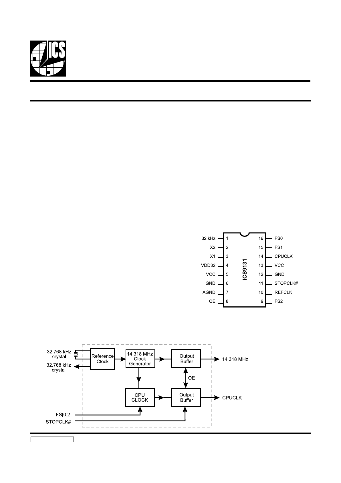
ICS9131
Block Diagram
32 KhZ Motherboard Frequency Generator
9131 Rev B 052897P
The ICS9131 offers a tiny footprint solution for generating
a selectable CPU clock from a 32.768 kHz crystal. The device
allows a variety of microprocessors to be clocked by changing
the state of address lines FS0, FS1, and FS2. The ICS9131 is
the ideal solution for replacing high speed oscillators and for
reducing clock speeds to save power in computers. The
device provides smooth, glitch-free frequency transitions so
that the CPU can continue to operate during slow down or
speed up. The rate of frequency change makes the ICS9131
compatible with all 386DX, 386SX, 486DX, 486DXZ, 486SX
and Pentium™ microprocessors.
The ICS9131 is driven from a single 32.768 kHz crystal. The
only external components required are the crystal and a 10M
ohm resistor. The device generates the 14.318 MHz system
clock, eliminating the need for a 14.318 MHz crystal. HighPerformance applications may require high speed clock
termination components.
• Single 32.768 kHz crystal generates system clock and
selectable CPU clock
• Generates CPU clocks from 8 MHz to 100 MHz.
• Operates from 3.3V or 5.0V supply
• Operates up to 66 MHz at 3.3V
• Separate VDD for 32 kHz clock enables it to run from
battery
• STOPCLK feature allows for a glitch-free turn-on and
Pen-turn-off of the CPU clock to static processors
• Output enable tristates outputs
• 16-pin PDIP or SOIC package
• Frequency selects allow for a smooth transition of
the CPUCLK
VDD32 Supply
The ICS9131 has a separate power supply for the 32.768 kHz
oscillator circuitry. This allows the 32 kHz clock to run from
a battery or other source while the main power to the chip is
disconnected. The VDD32 supply is guaranteed to operate
down to +2.0V, with the clock consuming less than 10µA at
+3.3V and the main VDD at 0V.
The frequencies and power-down options in the ICS9131 are
mask programmable. Customer specific masks can be made
and prototypes delivered within 6-8 weeks from receipt of
order. ICS also offers standard versions, such as those described in this data sheet.
Pentium is a trademark of Intel.
Pin Configuration
16-Pin DIP or SOIC
Page 2
2
ICS9131
Pin Descriptions
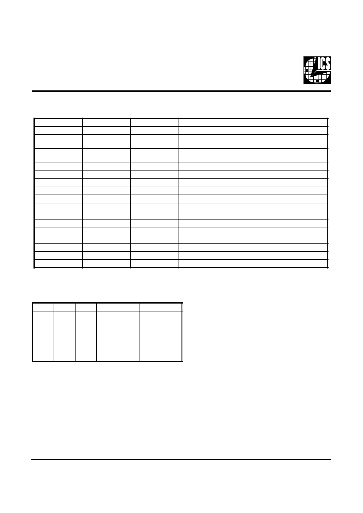
Functionality
FS2 FS1 FS0 CPUCLK ACTUALS
0
0
0
0
1
1
1
1
0
0
1
1
0
0
1
1
0
1
0
1
0
1
0
1
16
25
33.3
40
50
60
66.6
80
16.004
25.059
33.412
40.095
50.119
60.142
66.484
80.190
PIN NUMBER PIN NAME TYPE DESCRIPTION
1 32 kHz Output 32.768 kHz output.
2 X2 Output
Connect 32 kHz crystal, this input includes internal load
capacitor for crystal.
3 X1 Input
Connect 32 kHz crystal, this input includes internal load
capacitor for crystal.
4 VDD32 -- Power Supply for 32 kHz oscillator.
5 VCC -- Power Supply.
6 VSS -- Ground.
7 AGND -- Analog Ground.
8 OE Input OE tristates outputs when low.
9 FS2 Input CPU clock frequency select 2.
10 REFCLK Output 14.318 M Hz output.
11 STOPCLK# Input Stops CPU clock when low.
12 VSS -- Ground.
13 VCC -- Power supply.
14 CPUCLK Output CPU clock output (see Decoding table).
15 FS1 Input CPU clock frequency select 1.
16 FS0 Input CPU clock frequency select 0.
Page 3
3
ICS9131
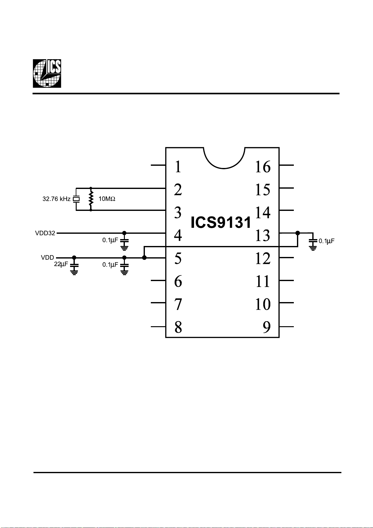
Recommended External Circuit
Notes:
1) The external components shown should be placed as close to the device as possible.
2) Pins 5 and 13 should be connected together externally. One decoupling capacitor may suffice for both pins.
Page 4

4
ICS9131
Electrical Characteristics at 5V
Absolute Maximum Ratings
VDD referenced to GND . . . . . . . . . . . . . . . . . . . . . . 7V
Operating temperature under bias. . . . . . . . . . . . . . . . 0°C to +70°C
Storage temperature . . . . . . . . . . . . . . . . . . . . . . . . . . -40°C to +150°C
Voltage on I/O pins referenced to GND. . . . . . . . . . . GND -0.5V to VDD +0.5V
Power dissipation . . . . . . . . . . . . . . . . . . . . . . . . . . . . 0.5 Watts
Stresses above those listed under Absolute Maximum Ratings may cause permanent damage to the device. This is a stress rating
only and functional operation of the device at these or any other conditions above those indicated in the operational sections
of the specifications is not implied. Exposure to absolute maximum rating conditions for extended periods may affect product
reliability.
Operating VDD = +4.5V to +5.5V; TA =0°C to 70°C unless otherwise stated
Note 1: Parameter is guaranteed by design and characterization. Not 100% tested in production.
Note 2: With the STOPCLK pin low (active).
Note 3: Absolute Jitter measured as the shortest and longest period difference to the mean period of the sample set.
DC Characteristics
PARAMETER SYMBOL TEST CONDITIONS MIN TYP MAX UNITS
Input Low Voltage V
IL
--0.8V
Input High Voltage V
IH
2.0 - - V
Input Low Current I
IL
VIN=0V -15.0 -6.0 µA
Input High Current I
IH
VIN=V
DD
-2.0 - 2.0 µA
Pull-up Resistor, Note 1 R
pu
VIN=VDD-1V - 400 700 k ohms
Output Low Current, Note 1 I
OL
V
OUT
=0. 8V 25 45 - mA
Output High Current, Note 1 I
OH
V
OUT
=2.0V - -53 -35 mA
Output Low Voltage V
OL
IOL=10mA - 0.15 0.4 V
Output High Voltage, Note 1 V
OH
IOH=-30mA 2.4 3.7 - V
Supply Current I
DD
No load, at 50 MHz - 18 35 mA
Output Frequency Change over
Supply and Temperature, Note 1
F
d
With respect to typical
frequency
- 0.002 0.05 %
Standby Supply Current, Note 2 I
DDSTDBY
Unloaded - 12 25 mA
Page 5

5
ICS9131
Electrical Characteristics at 5V
Operating VDD = +4.5V to +5.5V; TA =0°C to 70°C unless otherwise stated
Note 1: Parameter is guaranteed by design and characterization. Not 100% tested in production.
Note 2: With the STOPCLK pin low (active).
Note 3: Absolute Jitter measured as the shortest and longest period difference to the mean period of the sample set.
AC Characteristics
PARAM ETER SYMBOL TEST CONDITIONS MIN TYP MAX UNITS
Output Frequency, Note 1 f
o
Clock1 12.0 - 100 MHz
Input Frequency, Note 1 f
i
2.0 32 38 kHz
Output Rise time, Note 1 t
r
15pF load, 0.8 to 2.0V - 0.60 1.4 ns
Rise time, Note 1 t
r
15pF load, 20% to 80% V
DD
- 1.6 3. 0 ns
Output Fall time, Note 1 t
f
15pF load, 2.0 to 0.8V - 0.50 1.2 ns
Fall time, Note 1 t
f
15pF load, 80% to 20% V
DD
- 0.9 2. 5 ns
Duty cycle, Note 1 d
t
15pF load @1.4V 45 50 55 %
Jitter, 1 sigma from 33-80 MHz,
Note 1
T
jis
10,000 samples - 50 150 ps
Jitter, Absolute from 33-80 MHz,
Notes 1, 3
T
jabs
10,000 samples -250 - 250 ps
Jitter, 1 sigma from 16-25 MHz,
Note 1
T
jis
10,000 samples 60 150 ps
Jitter, Absolute from 16-25 MHz,
Note 1, 3
T
jabs
10,000 samples -600 - 600 ps
Jitter, 1 sigma from 14 to below,
Note 1
T
jis
10,000 samples - 1 3 %
Jitter, Absolute from 14 to below,
Note 1, 3
T
jabs
10,000 samples - 2 5 %
Frequency Transition time, Note 1 t
ft
2.0 5. 0 10. 0 ms
Power-up time, Note 1 t
pu
3.0 7. 5 15 ms
Page 6

6
ICS9131
Electrical Characteristics at 3.3V
Operating VDD = +3.3V to +3.7V; TA =0°C to 70°C unless otherwise stated
Note 1: Parameter is guaranteed by design and characterization. Not 100% tested in production.
Note 2: With the STOPCLK pin low (active).
Note 3: Absolute Jitter measured as the shortest and longest period difference to the mean period of the sample set.
DC Characteristics
PARAMETER SYMBOL TEST CONDITIONS MIN TYP MAX UNITS
Input Low Voltage V
IL
- - 0.2 V
DD
V
Input High Voltage V
IH
0.7 V
DD
--V
Input Low Current I
IL
VIN=0V -7.0 -2.5 µA
Input High Current I
IH
VIN=V
DD
-2.0 - 2.0 µA
Pull-up Resistor, Note 1 R
pu
VIN=VDD-1V - 600 900 k ohms
Output Low Current, Note 1 I
OL
V
OUT
=0.2V 15 2 4 - mA
Output High Current, Note 1 I
OH
V
OUT
=0.7V - -13 -8 mA
Output Low Voltage, Note 1 V
OL
IOL=60mA - 0.05 V
DD
0.1 V
DD
V
Output High Voltage, Note 1 V
OH
IOH=-4.0mA 6.85 V
DD
0.94 V
DD
-V
Supply Current I
DD
No load, at 50 MHz - 13 25 mA
Output Frequency Change over
Supply and Temperature, Note 1
F
d
With respect to typical
frequency
- 0.002 0.05 %
Standby Supply Current, Note 2 I
DDSTDBY
No load - 8 15 mA
AC Characteristics
Output Frequency, Note 1 f
o
Clock1 12.0 - 100 MHz
Input Frequency, Note 1 f
i
2.0 32 38 kHz
Rise time, Note 1 t
r
15pF load, 20% to 80% V
DD
- 2.2 3.5 ns
Fall time, Note 1 t
f
15pF load, 80% to 20% V
DD
- 1.2 2.5 ns
Duty cycle, Note 1 d
t
15pF load @50% V
DD
43 - 53 %
Jitter, 1 sigma , Note 1 T
jis
10,000 samples - 50 150 ps
Jitter, Absolute, Note 1, 3 T
jabs
10,000 samples -250 250 ps
Jitter, 1 sigma from 16-25 MHz T
jis
10,000 samples - 60 150 ps
Jitter, Absolute from 16-25 MHz T
jabs
10,000 samples -600 - 600 ps
Jitter, 1 sigma from 14 to below T
jis
10,000 samples - 1 3 %
Jitter, Absolute from 14 to below T
jabs
10,000 samples - 2 5 %
Frequency Transition time, Note 1 t
ft
6.7 14.0 ms
Power-up time, Note 1 t
pu
- 8.55 17.0 ms
Page 7

7
ICS9131
Stop Clock Feature
The ICS9131 incorporates a unique stop clock feature
compat-ible with static logic processors. When the stop
clock pin goes low, the CPUCLK will go low after the next
occuring falling edge. When STOPCLK again goes high,
CPUCLK resumes on the next rising edge of the internal
clock. This feature enables fast, glitch-free starts and stops
of the CPUCLK and is useful in Energy Star motherboard
applications.
32 kHz Supply Current
ADVANCE INFORMATION documents contain information on new products in the
sampling or preproduction phase of development. Characteristic data and other
specifications are subject to change without notice.
Page 8

8
ICS9131
Ordering Information
ICS9131-01CN16 or ICS9131-01CS16
Example:
ICS XXXX M X#W
16-Pin SOIC P acka ge
Lead Count & Package Width
Lead Count=1, 2 or 3 digits
W=.3” SOIC or .6” DIP; None=Standard Width
Package Type
N=DIP (Plastic)
S=SOIC
Device Type (consists of 3 or 4 digit numbers)
Prefix
ICS, A V=Standard Device
16-Pin DIP Pac kage
 Loading...