

Page 1
Integrated
Circuit
Systems, Inc.
General Description
Features
ICS9120-45
Low-Cost 8-Pin Frequency Generator
9120-45 Rev B 05/23/97
This data sheet (ICS9120-45) is an addedum to the existing ICS9120-08/09
data sheet. All information in this data sheet supersedes the data found in the
orginal ICS9120-08/09 data sheet.
The ICS9120-45 is a high performance frequency generator
designed to support the clock requirements of communication
and audio interfaces.
High accuracy, low-jitter PLLs meet the -96dB signal-tonoise ratios required by 16-bit audio systems. Fast output
clock edge rates minimize board induced jitter.
The on-chip XT AL oscillator accuracy is better than ±100ppm
for an AT cut, 18pF load crystal with initial accuracy of ppm
plus TC, aging and load variation of ±20ppm each assuming
33pF ±5% external load capacitors.
• Generates 32MHz, 40MHz and 48MHz
• Single 10 MHz crystal reference
• 49.92 MHz accuracy tracks 40.32 MHz reference
• 80ps one sigma jitter maintains 16-bit performance
• Output rise/fall times less than 1.5ns
• On-chip loop filter components
• 3.0-5.5V supply range
• 8-pin, 150-mil SOIC package
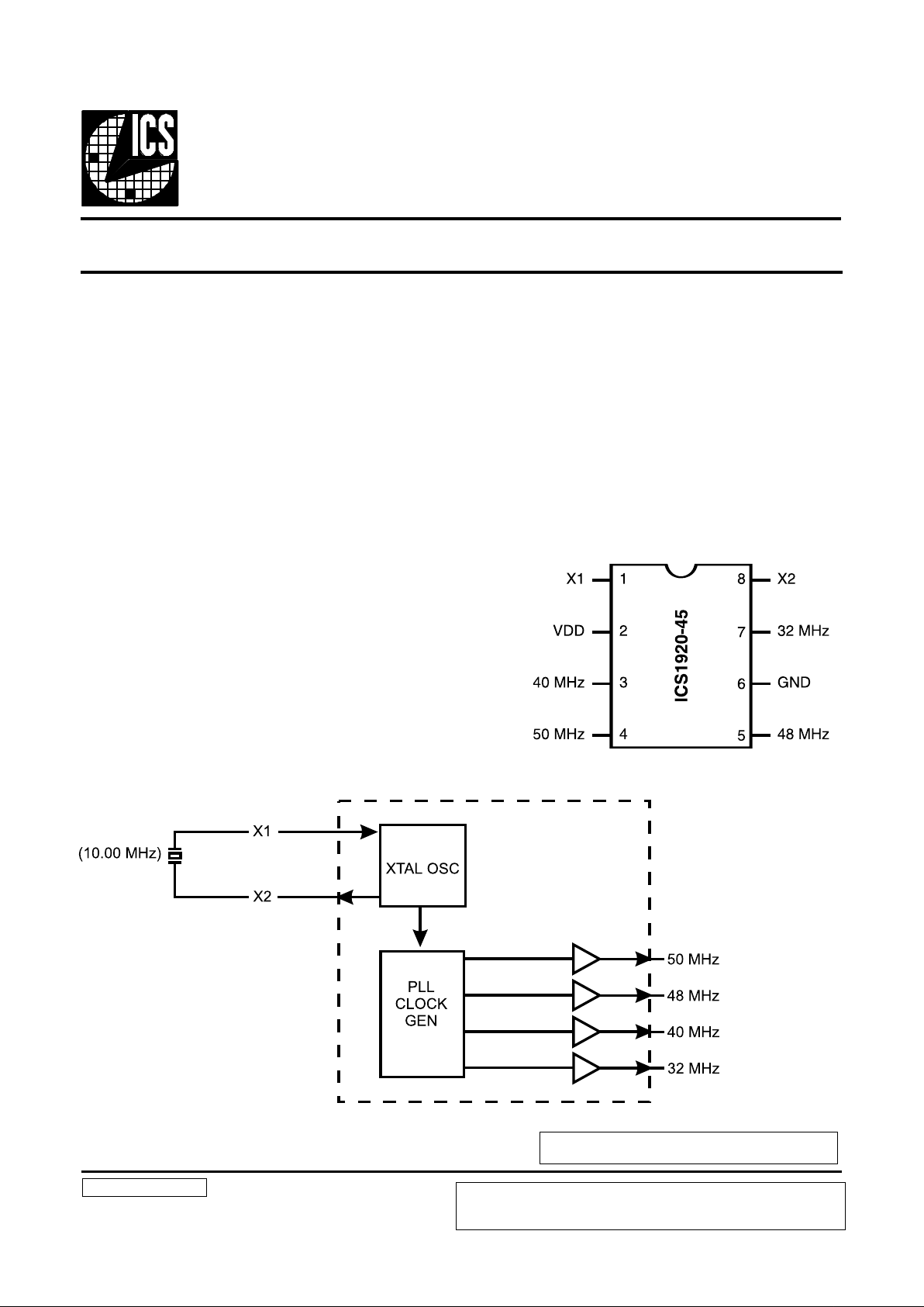
Pin Configuration
8 Pin SOIC
Block Diagram
ICS reserves the right to make changes in the device data identified in this
publication without further notice. ICS advises its customers to obtain the latest
version of all device data to verify that any information being relied upon by the
customer is current and accurate.
Page 2
2
ICS9120-45
Pin Descriptions
Note: The 10.00 MHz crystal that is connected to pin 1 and 8 is a parallel resonant component
that is designed to operate into a 8pF capacitive load. This device is a 5V power supply device.
PIN
NUMBER
PIN NAME TYPE DESCRIPTION
1 X1 Input 10.00 MHz input from crystal.
2 VDD Power +Power supply input.
3 40.00 MHz Output 40 MHz clock output.
4 50.00 MHz Output 50 MHz clock output.
5 48.00 MHz Output 48 MHz clock output.
6 GND Power Ground return for Pin 2.
7 32.00 MHz Output 32 MHz clock output.
8 X2 Output 10.00 MHz output.
Page 3

3
ICS9120-45
Absolute Maximum Ratings
Electrical Characteristics at 5 V
* Parameter is guaranteed by design and characterization. Not 100% tested in production.
Stresses above those listed under Absolute Maximum Ratings may cause permanent damage to the device. This is a stress
rating only and functional operation of the device at these or any other conditions above those indicated in the operational
sections of the specifications is not implied. Exposure to absolute maximum rating conditions for extended periods may
affect product reliability.
A V DD,VDD referenced to GND . . . . . . . . . . . . . . . . 7V
Operating temperature under bias. . . . . . . . . . . . . . . . 0°C to +70°C
Storage temperature . . . . . . . . . . . . . . . . . . . . . . . . . . -65°C to +150°C
Voltage on I/O pins referenced to GND. . . . . . . . . . . GND -0.5V to VDD +0.5V
Power dissipation . . . . . . . . . . . . . . . . . . . . . . . . . . . . 0.5 Watts
VDD = +4.5 to +5.5 V, TA = 0-70oC unless otherwise stated
DC Characteristics
PARAMETER SYMBOL TEST CONDITIONS MIN TYP MAX UNITS
Input Low Voltage
V
IL
--0.8V
Input High Voltage
V
IH
2.0 - - V
Input Low Current
I
IL
VIN=0V (For -09 only) - -8.3 -18.0 µ A
Input High Current
I
IH
VIN=VDD (For -09 only) - - 5. 0 µA
Output Low Voltage
V
OL
*
IOL=+10mA - 0.15 0.4 V
Output High Voltage
V
OH
*
IOH=-30mA 2.4 3. 7 - V
Output Low Current
I
OL
*
VOL=0.8V 25.0 45.0 - mA
Output High Current
I
OH
*
VOH=2.4V - -53.0 -35.0 mA
Supply Current
I
CC
Unloaded - 22.0 50.0 mA
Supply Current
I
CC
Unloaded (For -09 only) - 180.0 500.0 µ A
Pull-up Resistor Value
R
pu
*
(For -09 only) - 400.0 800.0 k ohm
AC Characteristics
Rise Time 0.8 to 2.0V
T
r
*
15pF load - 0. 9 2. 0 ns
Fall Time 2.0 to 0.8V
T
f
*
15pF load - 0. 7 1. 5 ns
Rise Time 20% to 80%
T
r
*
15pF load - 1. 8 3. 25 ns
Fall Time 80% to 20%
T
f
*
15pF load - 1. 4 2. 5 ns
Duty Cycle
D
t
* 15pF load @ 50% of VDD;
Except REFCLK
45.0 50.0 55. 0 %
Duty Cycle
D
t
* 15pf load @ 50% of VDD;
REFCLK only
40.0 50.0 60. 0 %
Jitter, One Sigma
T
jis
* For all frequencies except
REFCLK
- 85. 0 - ps
Jitter, Absolute
T
jab
For all frequencies except
REFCLK
-700.0 380.0 700.0 ps
Jitter, One Sigma
T
jis
*
REFCLK only - 266.0 600.0 ps
Jitter, Absolute
T
jab
REFCLK only -1.5 380.0 1.5 ns
Input Frequency
F
i
*
11.0 14.0 17. 0 MHz
Output Frequency
F
o
*
11.0 - 42.0 MHz
Power-up Time
T
pu
*
0 to 33.8 MHz - 5. 5 12. 0 ms
Crystal Input Capacitance
C
inx
*
X1 (Pin 1)# X2 (Pin 8; -08 only) - 5 - pF
Page 4

4
ICS9120-45
Electrical Characteristics at 3.3 V
* Parameter is guaranteed by design and characterization. Not 100% tested in production.
DC Characteristics
PARAMETER SYMBOL TEST CONDITIONS MIN TYP MAX UNITS
Input Low Voltage
V
IL
- - 0.2VDD V
Input High Voltage V
IH
0.7VDD - - V
Input Low Current I
IL
VIN=0V (For -09 only) - -3.6 -8.0 µ A
Input High Current I
IH
VIN=VDD (For -09 only) - - 5.0 µA
Output Low Voltage V
OL
* IOL=6mA - 0.05VDD 0.1 V
Output High Voltage V
OH
* IOH=-4.0mA 0.85VDD 0.94VDD - V
Output Low Current I
OL
* VOL=0. 2VDD 15.0 24.0 - mA
Output High Current I
OH
* VOH=0. 7VDD - -13.0 -8.0 mA
Supply Current I
CC
Unloaded - 13.0 32.0 mA
Supply Current I
CC
(PD) Unloaded (For -09 only) - 50.0 110.0 µ A
Pull-up Resistor Value R
pu
* (For -09 only) - 620.0 900.0 k ohm
AC Characteristics
Rise Time 0.8 to 2.0V Tr* 15pF load - 1.5 4.0 ns
Fall Time 2.0 to 0.8V T
f
* 15pF load - 1.0 3.0 ns
Rise Time 20% to 80% T
r
* 15pF load - 2.2 4.0 ns
Fall Time 80% to 20% T
f
* 15pF load - 1.5 3.0 ns
Duty Cycle D
t
*
15pF load @ 50% of VDD;
Except REFCLK
45.0 50.0 55.0 %
Duty Cycle D
t
*
15pF load @ 50% of VDD;
REFCLK only
40.0 45.0 60.0 %
Jitter, One Sigma T
jis
*
For all frequencies except
REFCLK
- 100.0 - ps
Jitter, Absolute T
jab
For all frequencies except
REFCLK
-900.0 380.0 900.0 ps
Jitter, One Sigma T
jis
* REFCLK only - 266.0 600.0 ps
Jitter, Absolute T
jab
REFCLK only -1.5 380.0 1.5 ns
Input Frequency F
i
* 11.0 14.3 15.0 MHz
Output Frequency F
o
* 11.0 - 38.0 MHz
Power-up Time T
pu
* 0 to 33.8 MHz - 5.5 12.0 ms
Crystal Input Capacitance C
inx
* X1 (Pin 1)# X2 (Pin 8; -08 only) - 5 - pF
Page 5

5
ICS9120-45
Ordering Information
ICS9120M-45
0.194
0.031
0.024
0.016
0.050
0.006
± 0.004
0.238
0.154
0.015
0.063
0.025
0.008
8-Pin SOIC Package
Example:
ICS XXXX M-PPP
Package Type
M =SOIC
Device Type (consists of 3 or 4-digit numbers)
Prefix
ICS, AV=Standard Device
Pattern Number (2 or 3-digit number for parts with ROM code pattern)
ICS reserves the right to make changes in the device data identified in this
publication without further notice. ICS advises its customers to obtain the latest
version of all device data to verify that any information being relied upon by the
customer is current and accurate.
 Loading...