

Page 1
Integrated
Circuit
Systems, Inc.
General Description
Features
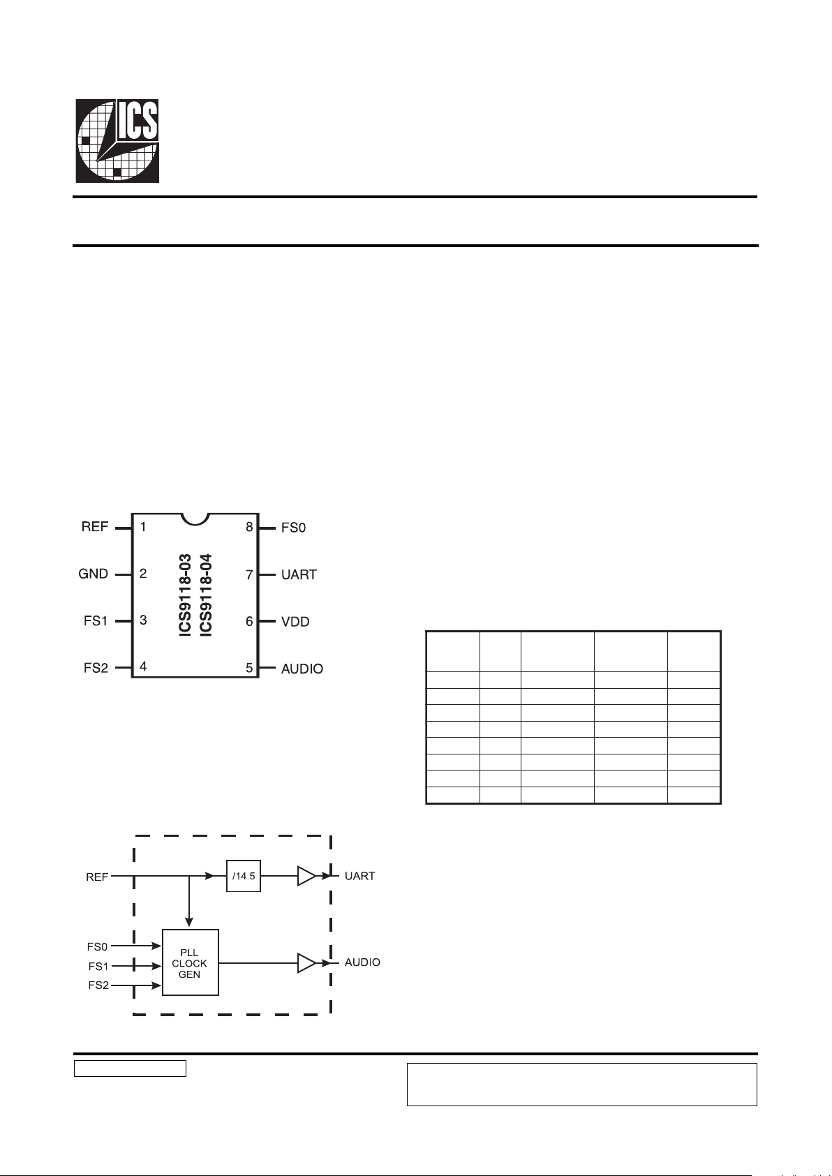
ICS9118-03
ICS9118-04
Frequency Generator for Digital Video Systems
9118-03 9118-04 RevB 7/28/99
Block Diagram
The ICS9118-03 and ICS9118-04 are low-cost, highperform-ance clock generators designed to support digital
video systems. 1.8MHz UART and AUDIO clocks are
generated from the recovered 27MHz reference signal.
The -03 supports 256x audio oversampling, and the -04
supports 384x audio oversampling.
The audio clock is synthesized from 27 MHz using a high
accuracy, low jitter PLL to meet the synchronization and
-96dB signal-to-noise ratios required by 16-bit DSP systems.
Fast output clock edge rates minimize board-induced jitter.
• Genreates AUDIO codec and UART clocks
synchronized to the 27MHz recovered video clock
• Selectable AUDIO clock supports 256x and 384x
over-sampling of 16.00, 22.05, 24.00, 32.00, 44.10
and 48.00 kHz
• 80ps one sigma jitter maintains 16 bit performance
• Output rise/fall times less than 1.5nS
• On chip loop filter components
• 3.0V - 5.5V supply range
• 8-pin, 150-mil SOIC package
Applications
• Specifically designed to support the high
performance clocking requirements of digital video
set-top and multi-media systems
Pin Configuration
8-Pin SOIC
Functionality
VDD=3.0-5.5V, TEMP=0-70°
FER
)zHM(
SF
]0:2[
OIDUA
30
)zHM(
OIDUA
40
)zHM(
TRAU
)zHM(
00.72000etatsirTetatsirTetatsirT
00.7210000.61*65200.61*4830268.1
00.7201050.22*65250.22*4830268.1
00.7211000.42*65200.42*4830268.1
00.7200100.23*65200.23*4830268.1
00.7210101.44*65201.44*4830268.1
00.7201100.84*65200.84*4830268.1
00.72111woLwoLwoL
ICS reserves the right to make changes in the device data identified in this
publication without further notice. ICS advises its customers to obtain the latest
version of all device data to verify that any information being relied upon by the
customer is current and accurate.
Obsolete
ICS9118-04 Obsolete
Page 2
2
ICS9118-03
ICS9118-04
Obsolete
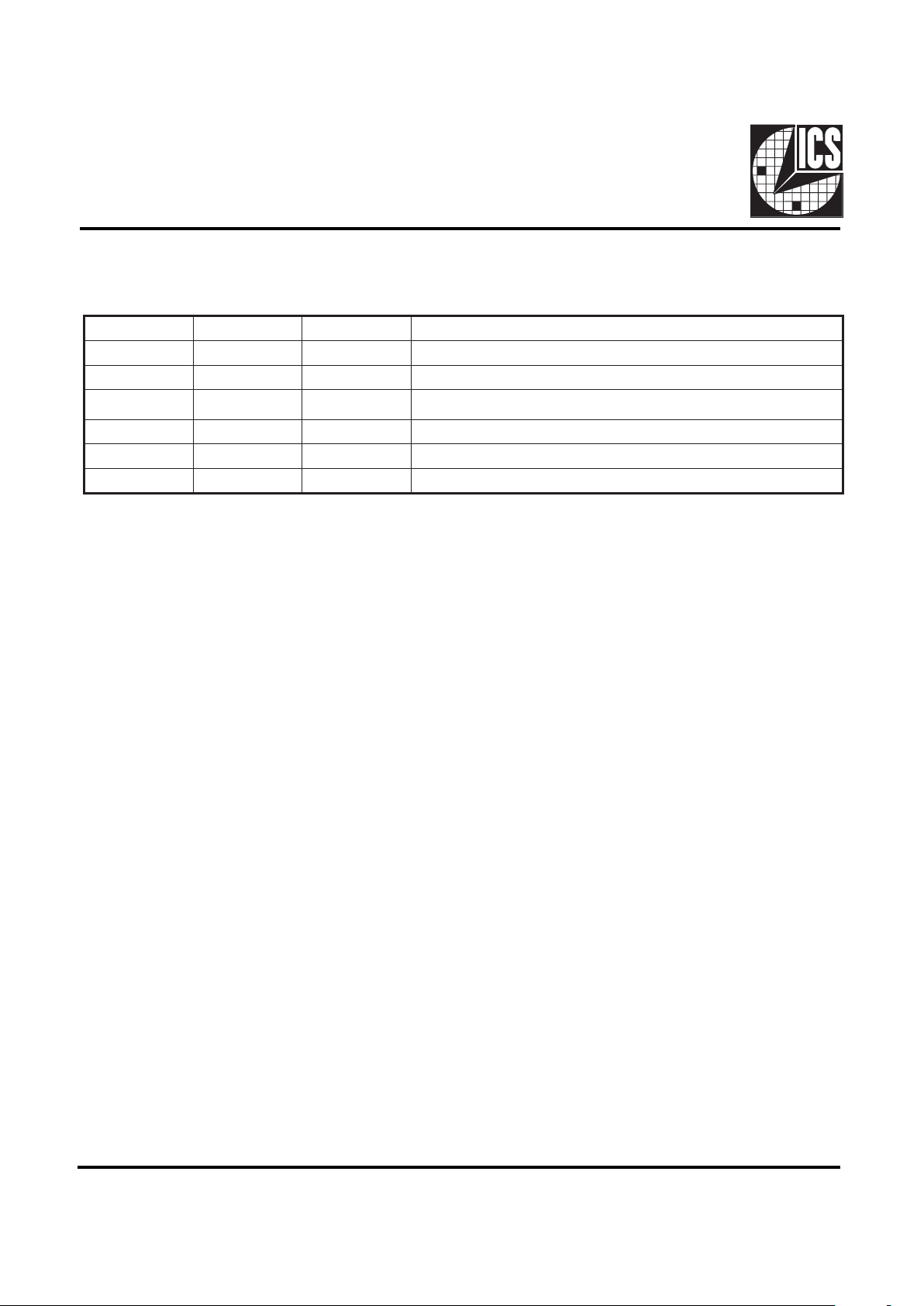
Pin Descriptions for ICS9118-01/02
REBMUNNIPEMANNIPEPYTNOITPIRCSED
1FERNIkcolctupniecnerefeRzHM0.72
2DNGRWPsreffubtuptuo,cigolrofdnorG
8,4,3)2:0(SFNI
evahstupniesehT.elbatytilanoitcnuFeeS.sniptcelesrelpitlumycneuqerF
.secivedpulluplanretni
5OIDUATUO.elbatytilanoitcnuFeeS.tuptuokcolcoiduA
6DDVRWP.sreffubtuptuoycneuqerfdexifdnaKLCP,cigolrofrewoP
7TRAUTUO.zHM0268.1tuodexiftuptuokcolcTRAU
Page 3

3
ICS9118-03
ICS9118-04
Obsolete
Absolute Maximum Ratings
Electrical Characteristics at 5V
Operation VDD = +4.5 to +5.5 V, TA = 0 to 70oC unless otherwise stated
*Parameter is guaranteed by design and characterization. Not 100% tested in production.
A VDD, VDD referenced to GND ...........................................................................7V
Operating temperature under bias...................................................... 0oC to +70oC
Storage temperature ....................................................................... -65oC to +150oC
Voltage on I/O pins referenced to GND ......................... GND -0.5V to VDD +0.5V
Power dissipation ......................................................................................0.5 Watts
Stresses above those listed under Absolute Maximum Ratings may cause permanent damage to the device. This is a stress
rating only and functional operation of the device at these or any other conditions above those indicated in the operational
sections of the specifications is not implied. Exposure to absolute maximum rating conditions for extended periods may affect
product reliability .
scitsiretcarahCCD
RETEMARAPLOBMYSSNOITIDNOCTSETNIMPYTXAMSTINU
egatloVwoLtupnIV
LI --8.0V
egatloVhgiHtupnIV
HI 0.2--V
tnerruCwoLtupnII
LI V NI V0=-3.80.81-Aµ
tnerruChgiHtupnII
HI V NI V= DD --0.5Aµ
egatloVwoLtuptuOV
LO *Am01+=LOI-51.04.0V
egatloVhgiHtuptuOV
HO *Am03-=HOI7.21.4-V
tnerruCwoLtuptuOI
LO *VLO V8.0=0.520.54-Am
tnerruChgiHtuptuOI
HO *VHO V4.2=-0.35-0.53-Am
tnerruCylppuSI
DD *dedaolnU-0.220.03Am
eulaVrotsiseRpu-lluP*upR-0.0040.008mhok
scitsiretcarahCCA
emiTesiR*rTV0.2ot8.0daolFp510.15.1sn
emiTllaFT
f*V8.0ot0.2daolFp510.15.1sn
emiTkcoLT
L*%08ot%02,daolFp510.01sm
elcyCytuDD
t*
fo%05@daolFp51
TRAUtpecxE;DDV
0.540.050.55%
elcyCytuDD
t*
fo%05@daolFp51
ylnoTRAU;DDV
0.040.540.05%
amgiSenO,rettiJT
sij *oiduA0.050.08sp
etulosbA,rettiJT
baj *oiduA003-003+sp
rettiJ, amgiSenOT
sij *TRAU,KLCFER0.10.3sp
etulosbArettiJT
baj *TRAU,KLCFER0.5-0.5+sn
emiTpu-rewoPT
up *zHM8.33ot0-5.28.4sm
ecnaticapaCtupnIlatsyrCC
xni *
)1niP(1X,
)8niP(2X
-81-Fp
Page 4

4
ICS9118-03
ICS9118-04
Obsolete
Electrical Characteristics at 3.3V
Operation VDD = +3.0 to +3.7 V, TA = 0 to 70oC unless otherwise stated
*Parameter is guaranteed by design and characterization. Not 100% tested in production.
scitsiretcarahCCD
RETEMARAPLOBMYSSNOITIDNOCTSETNIMPYTXAMSTINU
egatloVwoLtupnIV
LI
--8.0V
egatloVhgiHtupnIV
HI
0.2--V
tnerruCwoLtupnII
LI
VNIV0=-3.80.81-Aµ
tnerruChgiHtupnII
HI
VNIV=
DD
--0.5Aµ
egatloVwoLtuptuOV
LO
*Am01+=LOI-51.04.0V
egatloVhgiHtuptuOV
HO
*Am01-=HOI7.20.3-V
tnerruCwoLtuptuOI
LO
*VLOV8.0=0.520.54-Am
tnerruChgiHtuptuOI
HO
*VHOV4.2=-0.35-0.01-Am
tnerruCylppuSI
DD
*dedaolnU-0.410.52Am
eulaVrotsiseRpu-lluP*upR-0.0040.008mhok
scitsiretcarahCCA
emiTesiR*rTV0.2ot8.0daolFp510.15.1sn
emiTllaFT
f
*V8.0ot0.2daolFp510.15.1sn
emiTkcoLT
L
*%08ot%02,daolFp510.01sm
elcyCytuDD
t
*
fo%05@daolFp51
TRAUtpecxE;DDV
0.540.050.55%
elcyCytuDD
t
*
fo%05@daolFp51
ylnoTRAU;DDV
0.040.540.05%
amgiSenO,rettiJT
sij
*oiduA0.050.08sp
etulosbA,rettiJT
baj
*oiduA003-003+sp
rettiJ, amgiSenOT
sij
*TRAU,KLCFER0.10.3sp
etulosbArettiJT
baj
*TRAU,KLCFER0.5-0.5+%
emiTpu-rewoPT
up
*zHM8.33ot0-5.25.4%
ecnaticapaCtupnIlatsyrCC
xni
*
)1niP(1X,
)8niP(2X
-81-Fp
Page 5

5
ICS9118-03
ICS9118-04
Obsolete
Ordering Information
ICS9118M-03
Example:
ICS XXXX M-PPP
Package Type
M =SOIC
Device Type (consists of 3 or 4-digit numbers)
Prefix
ICS, AV=Standard Device
Pattern Number (2 or 3-digit number for parts with ROM code pattern)
8 Pin SOIC Package
ADVANCE INFORMATION documents contain information on
new products in the sampling or preproduction phase of development. Characteristic data and other specifications are subject to
change without notice.
 Loading...