

Page 1
Integrated
Circuit
Systems, Inc.
General Description
Features
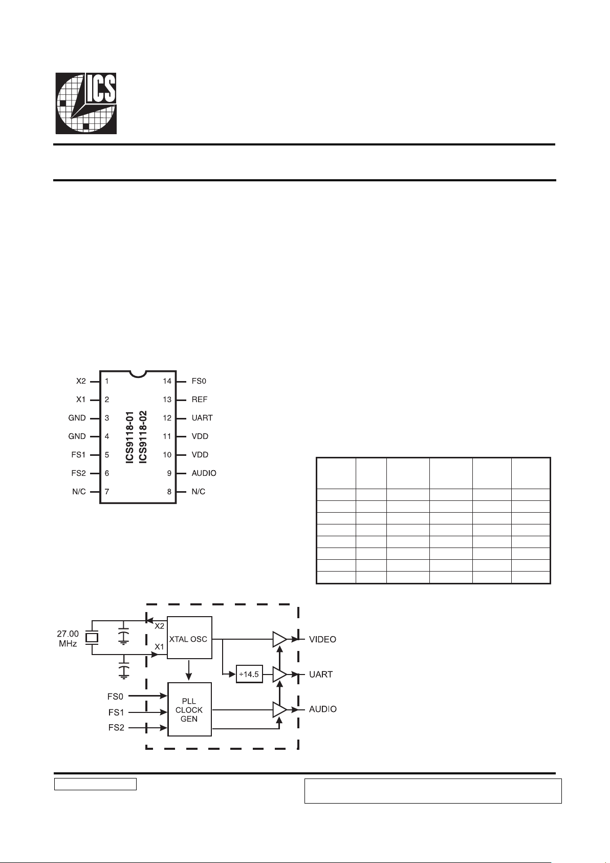
ICS9118-01
ICS9118-02
Frequency Generator for Digital Video Systems
9118-01 9118-02 RevB 7/27/99
Block Diagram
The ICS9118-01 and ICS9118-02 are low-cost, highperform-ance clock generators designed to support digital
video sys-tems. 27 MHz VIDEO, 1.8 MHz UART and
AUDIO clocks are generated from the recovered 27 MHz
signal. The on-chip crystal oscillator can be used in
conjunction with an exter-nal D/A conversation circuit to
provide ±130 ppm clock recovery using a standard 27
MHz crystal (contact ICS for application details).
The audio clock is synthesized from 27 MHz using a high
accuracy, low jitter PLL to meet the synchronization and
-96dB signal-to-noise ratios required by 16-bit DSP systems.
Fast output clock edge rates minimize board-induced jitter.
• Generates 27 MHz VIDEO, 1.8 MHz UAR T and
synchronous AUDIO codec clocks
• Selectable AUDIO clock supports 256x and 384x
over-sampling of 16.00, 22.05, 24.00, 32.00, 44.10
and 48.00 kHz
• On-chip crystal oscillator enables 27 MHz
clock recovery
• 80ps one sigma jitter maintains 16-bit performance
• 3.0V - 5.5V supply range
• 14-pin, 150-mil SOIC package
Applications
• Specifically designed to support the high
performance clocking requirements of digital video
set-top and multi-media systems
Pin Configuration
14-Pin SOIC
2X,1X
)zHM(
SF
]0:2[
OIDUA
10
)zHM(
OIDUA
20
)zHM(
FER
)zHM(
TRAU
)zHM(
00.72000etatsirTetatsirTetatsirTetatsirT
00.72100690.4441.600.720268.1
00.72010446.52.764.800.720268.1
00.72110441.6612.900.720268.1
00.72001291.8882.2100.720268.1
00.72101982.112.439.6100.70268.1
00.72011882.21234.8100.720268.1
00.72111woLwoLwoLwoL
Functionality
VDD=3.0-5.5V, TEMP=0-70°
PRODUCT PREVIEW documents contain information on products in the formative or
design phase development. Charactersitic data and other specifications are design
goals. ICS reserves the right to change or discontinue these procucts without notice.
Obsolete
ICS9118-02 Obsolete
Page 2
2
ICS9118-01
ICS9118-02
Obsolete
Pin Descriptions for ICS9118-01
REBMUNNIPEMANNIPEPYTNOITPIRCSED
12XTUO.ecnaticapacdaolLATXsedulcnihcihwtuptuoLATX
21XNI
LATXsedulcnitupnisihT.tupniycneuqerfecnereferlanretxeroLATX
zHM0.72yllanimronsaibkcabdeefdnaecnaticapacdaol
4,3SSVRWP.sreffubtuptuoycneuqerfdexifdnaKLCP,cigolrofdnuorG
41,6,5)2:0(SFNI
evahstupniesehT.elbatytilanoitcnuFeeS.sniptcelesreilpitlumycneuqerF
.secivedpulluplanretni
7C/N- .detcennocyllanretnitoN
8C/N- .detcennocyllanretnitoN
9OIDUATUO.elbatytilanoitcnuFeeS.tuptuokcolcoiduA
11,01DDVRWP.sreffubtuptuoycneuqerfdexifdnaKLCP,cigolrofrewoP
21TRAUTUO.zHM0268.1tuodexiftuptuokcolcTRAU
31FERTUO.zHM00.72tuodexiftuptuokcolcoediV
Page 3

3
ICS9118-01
ICS9118-02
Obsolete
Absolute Maximum Ratings
*Parameter is guaranteed by design and characterization. Not 100% tested in production.
AVDD, VDD referenced to GND ...................................................................... 7V
Operating temperature under bias................................................ 0oC to +70oC
Storage temperature..................................................................-65oC to +150oC
Voltage on I/O pins referenced to GND ............... GND -0.5V to VDD +0.5V
Power dissipation ................................................................................... 0.5 Watts
Stresses above those listed under Absolute Maximum Ratings may cause permanent damage to the device. This is a stress
rating only and functional operation of the device at these or any other conditions above those indicated in the operational
sections of the specifications is not implied. Exposure to absolute maximum rating conditions for extended periods may
affect product reliability.
scitsiretcarahCCD
RETEMARAPLOBMYSSNOITIDNOCTSETNIMPYTXAMSTINU
egatloVwoLtupnIV
LI
-- 8.0V
egatloVhgiHtupnIV
HI
0.2--V
tnerruCwoLtupnII
LI
VNIV0=-0.01-81-
m
A
tnerruChgiHtupnII
HI
VNIV=
DD
-- 0.5
m
A
egatloVwoLtuptuOV
LO
*ILOAm01+=-51.04.0V
egatloVhgiHtuptuOV
HO
*IHOAm01-=4.20.3-V
tnerruCwoLtuptuOI
LO
*V8.0=V0.020.53-Am
tnerruChgiHtuptuOI
HO
*V4.2=V-0.02-0.01-Am
tnerruCylppuSI
CC
%01±V3.3=DDV-0.410.52Am
eulaVrotsiseRpu-lluPR
up
*-0.0040.008mhok
scitsiretcarahCCA
emiTesiRT
r
*V0.2ot8.0daolFp51-0.15.1sn
emiTllaFT
f
*V8.0ot0.2,daolFp51-0.15.1sn
emiTkcoLT
L
*%08ot%02,daolFp510.01sm
elcyCytuDD
t
*
;DDVfo%05@daolFp51
TRAUtpecxE
0.540.050.55%
elcyCytuDD
t
*
;DDVfo%05@daolFp51
TRAUtpecxE
0.040.540.05%
aemgiSenO,rettiJT
s1j
*oiduA0.050.08sp
etulosbA,rettiJT
baj
*oiduA0.003-0.003+sp
amgiSenO,rettiJT
s1j
*TRAU,KLCFER0.10.3%
etulosbA,rettiJT
baj
*TRAU,KLCFER0.5+%
ycneuqerFnaeMtuptuO
tegraT.svycaruccA
F
ao
*tupnizHM0.72htiW0.08-0.08+mpp
emiTpu-rewoPT
up
*
fognissorcts1otV6.1=DDVmorF
.tceleSoiduA
.sm04<pmaRylppusDDV
5.25.4sm
ecnaticapaCtupnIlatsyrCC
xni
*
)1niP(1X
)8niP(2X
0.81Fp
Electrical Characteristics at 3.3V
Operating VDD = +3.0 V to +3.7V ; TA = 0 ºC to 70oC unless otherwise stated
Page 4

4
ICS9118-01
ICS9118-02
Obsolete
Electrical Characteristics at 5 V
VDD = +4.5 to +5.5 V, TA = 0 to 70oC unless otherwise stated
scitsiretcarahCCD
RETEMARAPLOBMYSSNOITIDNOCTSETNIMPYTXAM
STINU
egatloVwoLtupnIV
LI
--8.0V
egatloVhgiHtupnIV
HI
0.2--V
tnerruCwoLtupnII
LI
VNIV0=-3.80.81-Aµ
tnerruChgiHtupnII
HI
VNIV=
DD
--0.5Aµ
egatloVwoLtuptuOV
LO
*ILOAm01+=-51.04.0V
egatloVhgiHtuptuOV
HO
*IHOAm03-=7.21.4-V
tnerruCwoLtuptuOI
LO
*VLOV8.0=0.520.54-Am
tnerruChgiHtuptuOI
HO
*VHOV4.2=-0.35-0.53-Am
tnerruCylppuSI
DD
*dedaolnU-0.2203Am
eulaVrotsiseRpu-lluP*upR-0.0040.008mhok
scitsiretcarahCCA
emiTesiR*rTV0.2ot8.0daolFp510.15.1sn
emiTllaFT
f
*V8.0ot0.2daolFp510.15.1sn
emiTkcoLT
L
*%08ot%02,daolFp510.01sm
elcyCytuDD
t
*
fo%05@daolFp51
V
DD
TRAUtpecxE;
0.540.050.55%
elcyCytuDD
t
*
fo%05@daolFp51
V
DD
ylnoTRAU;
0.040.540.05%
amgiSenO,rettiJT
s1j
*oiduA0.050.08sp
etulosbA,rettiJT
baj
*oiduA003-003+sp
rettiJ, amgiSenOT
s1j
*TRAU,KLCFER0.13%
etulosbArettiJT
baj
*TRAU,KLCFER0.5-5+%
ycneuqerFnaeMtuptuO
tegraT.svycaruccA
F
ao
*tupnizHM813.41htiW0.08-0.08+mpp
emiTpu-rewoPT
up
*
.gnissorcts1otV6.1=DDVmorF
.sm04<pmaRylppusDDV
5.25.4sm
ecnaticapaCtupnIlatsyrCC
xni
*
)1niP(1X,
)8niP(2X
81Fp
Page 5

5
ICS9118-01
ICS9118-02
Obsolete
Ordering Information
ICS9118M-01
Example:
ICS XXXX M-PPP
Package Type
M =SOIC
Device Type (consists of 3 or 4-digit numbers)
Prefix
ICS, AV=Standard Device
Pattern Number (2 or 3-digit number for parts with ROM code pattern)
14 Pin SOIC Package
PRODUCT PREVIEW documents contain information on products in the formative or
design phase development. Charactersitic data and other specifications are design
goals. ICS reserves the right to change or discontinue these procucts without notice.
 Loading...