

Page 1
Integrated
Circuit
Systems, Inc.
General Description
Features
XTAL
OSC
PCLK
UCLK
MCLK
PLL
CLOCK
GEN
÷8
X2
14.7456
MHz
X1
PD
•
Generates the 14.7456 MHz microcontroller, 40.320
MHz datadump and 1.84320 UART clocks
• Less than ±80 ppm frequency variation including
temperature, voltage, load and aging tolerances
• Single crystal reference minimizes crystal reliability
and inventory issues
• 80 ps one sigma jitter maintains 16-bit performance
• Output rise/fall times less than 1.5 ns
• On-chip loop filter components
• 3.0 V - 5.5 V supply range
• 8-pin, 150-mil SOIC package
Applications
• Specifically designed to support the high performance
of fax/data modems
9117-01 RevA 052297P
Pentium is a trademark of Intel Corporation
PowerPC is a trademark of Motorola Corporation
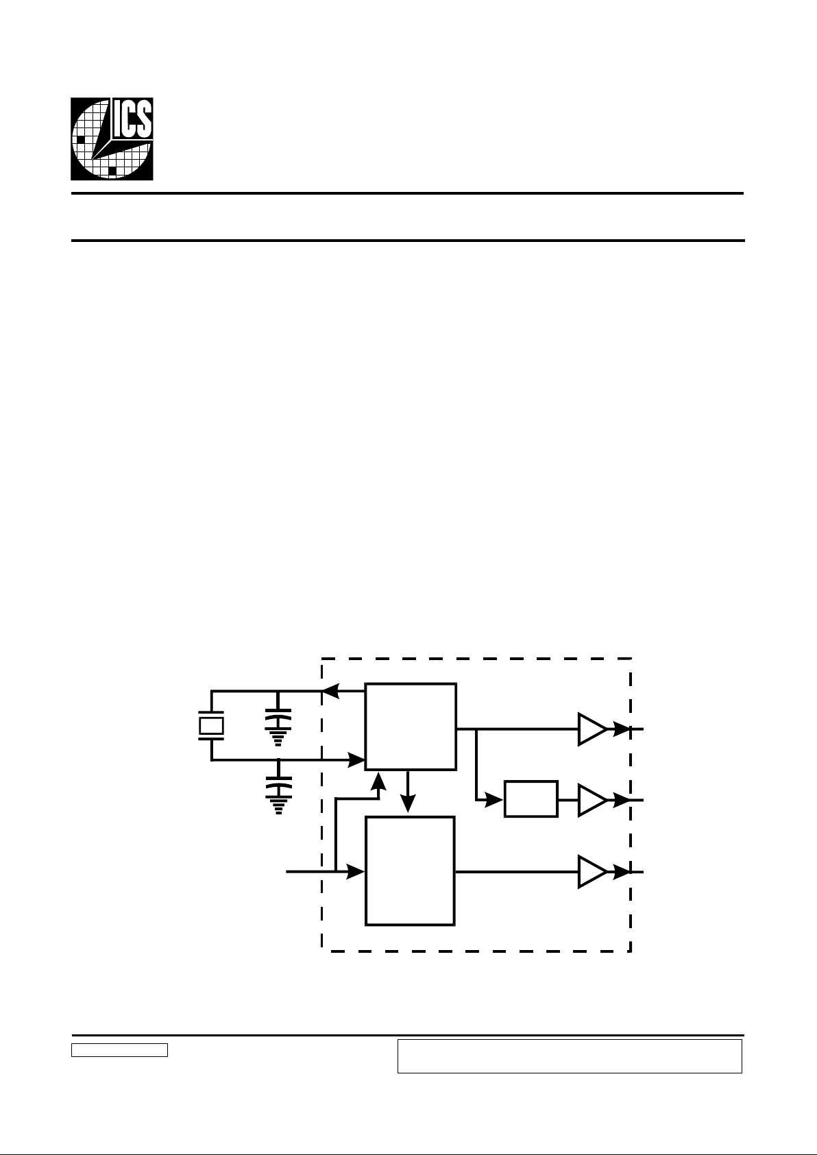
Frequency Generator for Modem Systems
ICS9117-01
The ICS9117-01 is a low-cost, high-performance frequency
generator designed to support fax/data modem systems.
Datapump and UART clocks are synthesized from a
microcontroller crystal using high-accuracy, low-jitter PLLs,
meeting the frequency tolerance and -96dB signal-to-noise
ratios required by 16-bit DSP modem systems. Fast output
clock edge rates minimize boar d induced jitter.
Exact frequency multiplying ratios ensure better than ±80
ppm frequency accuracy using a standard AT crystal with
external load capacitors (typically 33pF ±5% for an 18pF
series load crystal). Achieving ±80ppm over four years
requires the crystal to have 20 ppm initial accuracy , ±20 ppm
temperature and ±5 ppm/year aging coefficients.
Block Diagram
PRODUCT PREVIEW documents contain information on products in the formative or
design phase development. Charactersitic data and other specifications are design
goals. ICS reserves the right to change or discontinue these procucts without notice.
Page 2
2
ICS9117-01
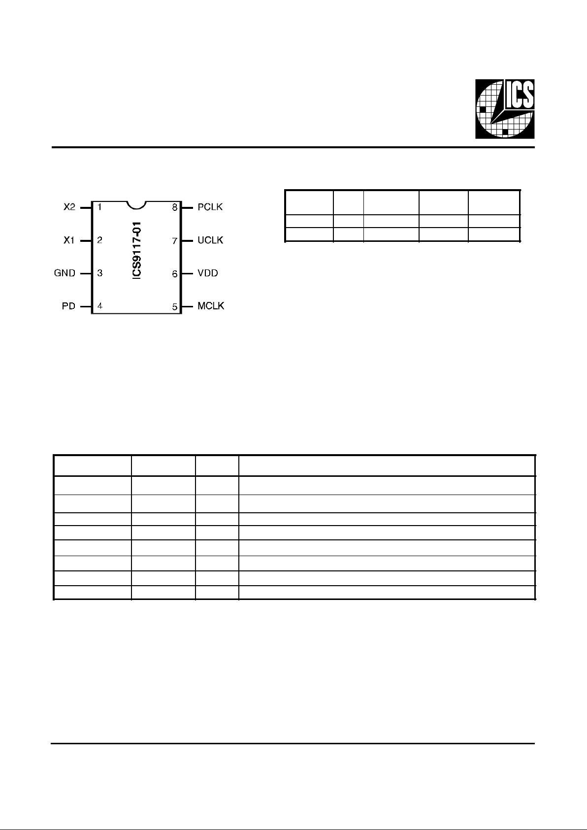
Pin Configuration
Pin Descriptions
Functionality
X1, X2
(MHz)
PD PCLK
(MHz)
MCL K
(MHz)
UCLK
(MHz)
14.7456 0 14.7456 40.320 1.8432
14. 7 45 6 1 L ow Low Low
PIN NU MBE R PIN NA ME TYP E DES CRI PT ION
1 X2 OUT Drive to crystal.
2 X1 IN Crystal or clock input.
3 GND PWR P ower s upp ly gr ound .
4 PD IN Power-down signal. Power-down all loops and oscilla tors.
5 MCLK OUT Dat ap ump 40 .32 MHz cl ock outp ut.
6 VDD PWR + 5V powe rs upp ly
7 UCLK OUT UART 1.84 MHz data cloc k output.
8 PCLK OUT Microcontroller 14.7 MHz clock output.
8-PIN SOIC
Page 3

3
ICS9117-01
Absolute Maximum Ratings
Electrical Characteristics at 3.3V
Stresses above those listed under Absolute Maximum Ratings may cause permanent damage to the device. This is a
stress rating only and functional operation of the device at these or any other conditions above those indicated in the
operational sections of the specifications is not implied. Exposure to absolute maximum rating conditions for
extended periods may affect product r eliability.
AVDD, VDD referenced to GND ----------------------------------------- 7V
Operating temperature under bias------------------------------------- 0 ºC to +70 ºC
Storage temperature------------------------------------------------------ -65 ºC to +150 ºC
Voltage on I/O pins referenced to GND ------------------------------ GND - 0.5 V to VDD + 0.5 V
Power dissipation --------------------------------------------------------- 0.5 Watts
Operating VDD = +3.0 V to +3.7V; TA = 0 ºC to 70oC unless otherwise stated
* Parameter is guaranteed by design and characterization. Not 100% tested in production.
DC Ch ar ac ter ist i cs
PARA M E TE R SYM B O L TE S T C O N DITI O NS MI N TYP MA X UNI T S
Input Low Voltage V
IL
--0.8V
Input High Voltage V
IH
2.0 - - V
Input Low Current I
IL
VIN=0V - -10.0 -25.0
µA
Input High Current I
IH
VIN=V
DD
- - 5.0
µA
Output Low Voltage VOL*IOL=+10mA - 0.15 0.4 V
Output High Voltage VOH*IOH=-10mA 2.4 3.7 - V
Output Low Current IOL* V=0.8V 20.0 35.0 - mA
Output High Current IOH* V=2.4V - -20.0 -10.0 mA
Supply Current I
CC
Unloaded - 16.0 30.0 mA
Pull- u p Re s istor V al ue Rpu* - 400.0 800.0 k ohm
AC Ch ar ac ter ist i cs
Rise Time Tr* 15o/f kiadm 0.8 to 2.0V - 0.9 1.5 ns
Fall T ime Tf* 15pF load, 2.0 to 0.8V - 1.2 3.0 ns
Lock Time TL* 15pFl oad, 20%to 80% 10.0 ms
Duty Cycle Dt*
15pFl oad @50% of VDD;
ExceptREFCLK
45.0 50.0 55.0 %
Duty Cycle Dt*
15pF load@50% of VDD;
Except REFCLK only
45.0 50.0 55.0 %
Jitte r, One Sigmea T
j1s
*
For all fr eque ncie s exce pt
REFCLK
70.0 100.0 ps
Jitte r, Absolute T
jab
*
Forall frequencies except
REFCLK
-300.0 +300.0 ps
Jitte r, One Sigma T
j1s
* REFCLK only 250.0 300.0 ps
Jitte r, Absolute T
jab
* REFCLK only -500.0 +500.0 ps
Input FrequencyRange Fi* 4.0 28.0 MHz
Output Fr equency Range Fo* 11. 7 74. 0 MHz
OutputMean Fre quency
Accur acy vs.Target
Foa* With 14.318 MHzinput -80.0 +80.0 ppm
Power-up Time Tpu* 0 to 33.8 MHz 2.5 4.5 ms
Crystal In put Capacita nce C
inx
*
X1 (Pin 1)
X2 (Pin 8)
18.0 pF
Page 4

4
ICS9117-01
Absolute Maximum Ratings
Electrical Characteristics at 5.0V
Stresses above those listed under Absolute Maximum Ratings may cause permanent damage to the device. This is a
stress rating only and functional operation of the device at these or any other conditions above those indicated in the
operational sections of the specifications is not implied. Exposure to absolute maximum rating conditions for
extended periods may affect product r eliability.
Operating VDD = +4.5 V to +5.5V; TA = 0 ºC to 70oC unless otherwise stated
AVDD, VDD referenced to GND ----------------------------------------- 7V
Operating temperature under bias------------------------------------- 0 ºC to +70 ºC
Storage temperature------------------------------------------------------ -65 ºC to +150 ºC
Voltage on I/O pins referenced to GND ------------------------------GND - 0.5 V to VDD + 0.5 V
Power dissipation --------------------------------------------------------- 0.5 Wa tts
DC Ch ar ac ter ist i cs
PARA M E TE R SYM B O L TE S T C O N DITI O NS MI N TYP MA X UNI T S
Input Low Voltage V
IL
--0.8V
Input High Voltage V
IH
2.0 - - V
Input Low Current I
IL
VIN=0V - -7.0 -25.0
µA
Input High Current I
IH
VIN=V
DD
- - 5.0
µA
Output Low Voltage VOL*IOL=+10mA - 0.15 0.4 V
Output High Voltage VOH*IOH=-10mA 4.0 4.2 - V
Output Low Current IOL* V=0.8V 20.0 40.0 - mA
Output High Current IOH* V=2.4V - -85.0 -65.0 mA
Supply Current I
CC
Unloaded - 22.0 -35.0 mA
Pull- u p Re s istor V al ue Rpu* - 400.0 800.0 k ohm
AC Ch ar ac ter ist i cs
Rise Time Tr* 15o/f kiadm 0.8 to 2.0V - 0/8 1.5 ns
Fall T ime Tf* 15pF load, 2.0 to 0.8V - 1.2 3.0 ns
Lock Time TL* 15pFl oad, 20%to 80% 10.0 ms
Duty Cycle Dt*
15pFl oad @50% of VDD;
Except REFCLK
45.0 50.0 55.0 %
Duty Cycle Dt*
15pF load@50% of VDD;
REFCLK only
45.0 50.0 55.0 %
Jitte r, One Sigmea T
j1s
*
For all fr eque ncie s exce pt
REFCLK
80.0 120.0 ps
Jitte r, Absolute T
jab
*
Forall frequencies except
REFCLK
-310.0 +300.0 ps
Jitte r, One Sigma T
j1s
* REFCLK only 200.0 250.0 ps
Jitte r, Absolute T
jab
* REFCLK only -500.0 +500.0 ps
Input FrequencyRange Fi* 5.0 43.0 MHz
Output Fr equency Range Fo* 14.0 114.0 MHz
OutputMean Fre quency
Accur acy vs.Target
Foa* With 14.318 MHzinput -80.0 +80.0 ppm
Power-up Time Tpu* 0 to 33.8 MHz 2.5 4.5 ms
Crystal In put Capacita nce C
inx
*
X1 (Pin 1),
X2 (Pin 8)
18.0 pF
* Parameter is guaranteed by design and characterization. Not 100% tested in production.
Page 5

5
ICS9117-01
Ordering Information
ICS9117M-01
0.194
0.031
0.024
0.016
0.050
0.006
± 0.004
0.238
0.154
0.015
0.063
0.025
0.008
8-Pin SOIC
Example:
ICS XXXX M-PPP
Package Type
M =SOIC
Device Type (consists of 3 or 4-digit numbers)
Prefix
ICS, AV=Standard Device
Pattern Number (2 or 3-digit number for parts with ROM code pattern)
PRODUCT PREVIEW documents contain information on products in the formative or
design phase development. Charactersitic data and other specifications are design
goals. ICS reserves the right to change or discontinue these procucts without notice.
 Loading...