

Page 1
Integrated
Circuit
Systems, Inc.
General Description Features
ICS9112-27
Preliminary Product Preview
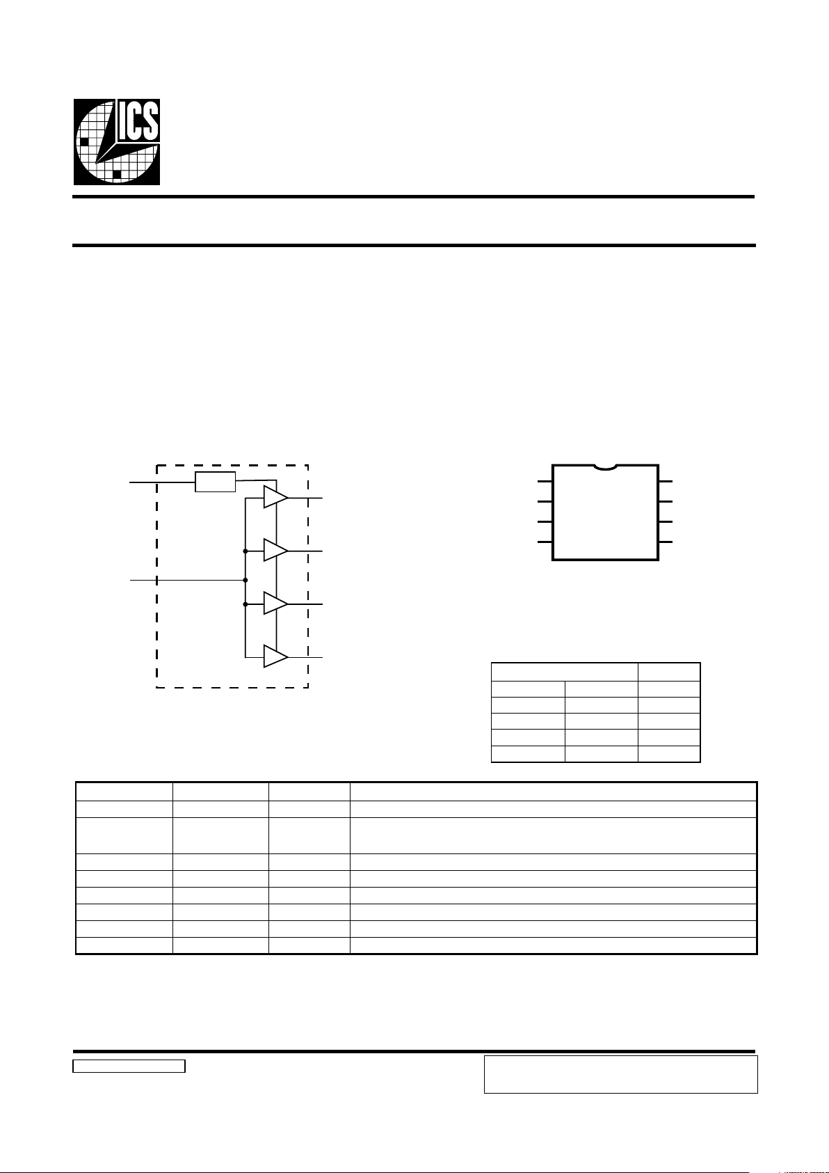
Block Diagram
Low Skew PCI / PCI-X Buffer
9112-27 Rev B 02/27/01
Pin Configuration
• Frequency range 0 - 140 MHz (3.3V)
• Less than 200 ps Jitter between outputs
• Skew controlled outputs < 100 ps
• Distribute one clock input to one bank of four
outputs
• 3.3V ±10% operation
• Available in 8 pin TSSOP, and SOIC packages.
The ICS9112-27 is a high performance, low skew, low jitter
PCI / PCI-X clock driver. It is designed to distribute high
speed signals in PCI / PCI-X applications operating at speeds
from 0 to 140 MHz.
The ICS9112-27 is characterized for operation from -40°C to
85°C for automotive and industrial applications.
8 pin TSSOP & SOIC
CLK_IN
OE
CLK0
GND
CLK3
CLK2
VDD
CLK1
ICS9112-27
1
2
3
4
8
7
6
5
CLK_IN
CLK0
CLK1
CLK2
CLK3
LOGIC
CONTROL
OE
Pin Descriptions
REBMUNNIPEMANNIPEPYTNOITPIRCSED
1NI_KLCNI.ycneuqerfecnerefertupnI
2EONI
kcolcehtsetatsirtti,wolsiEOnehw).pu_lluplanretnisah(elbanetuptuO
stuptuo
30KLCTUOtuptuokcolcdereffuB
4DNGRWPdnuorG
51KLCTUOtuptuokcolcdereffuB
6DDVRWPV3.3rofylppusrewoP
72KLCTUOtuptuokcolcdereffuB
83KLCTUOtuptuokcolcdereffuB
STUPNISTUPTUO
NI_KLCEO)0:3(KLC
000
010
100
111
Functionality Table
PRODUCT PREVIEW documents contain information on new
products in the sampling or preproduction phase of development.
Characteristic data and other specifications are subject to change
without notice.
Page 2
2
ICS9112-27
Preliminary Product Preview
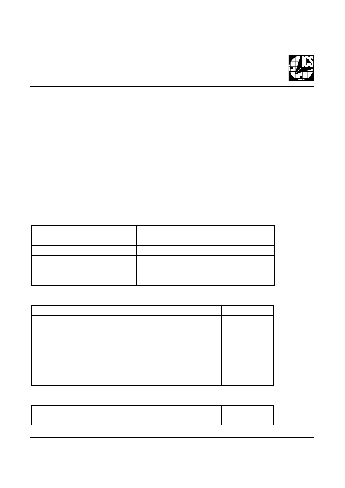
Absolute Maximum Ratings
Supply voltage range V
DD
. . . . . . . . . . . . . . . . . . . . . . . . . . . . . . . . . . . .
-0.5V to 4.3 V
Input voltage rangeV
I
(see notes 1 & 2) . . . . . . . . . . . . -0.5V to VDD + 0.5V
Output voltage range V
O
(see notes 1 & 2) . . . . . . . . . -0.5V to VDD + 0.5V
Input clamp current I
IK (VI
< 0 or VI >VDD) . . . . . . . . . . . . . . . . . . . ±50 mA
Output clamp current I
OK
(VO< 0 or VO) . . . . . . . . . . . . . . . . . . . . . . ±50 mA
Continuous total output current, I
O (VO
= 0 to VDD) . . . . . . . . . . . ±50 mA
Package thermal impedance Ø
JA
(see note 3): PW package . . . 230.5°C/W
Storage temperature rante, T
stg
. . . . . . . . . . . . . . . . . . . . . . . . . . . . . .
-65°C to 150°C
Stresses above those listed under Absolute Maximum Ratings may cause permanent damage to the device. These ratings are
stress specifications only and functional operation of the device at these or any other conditions above those listed in the
operational sections of the specifications is not implied. Exposure to absolute maximum rating conditions for extended
periods may affect product reliability.
Notes:
1. The input and output negative-voltage ratings may be exceeded if the input and output clamp-current ratings are
observed.
2. This value is limited to 4.6 V maximum.
3. The package thermal impedance is calculated in accordance with JESD 51.
snoitcnuFlanimreT
lanimreToNO/InoitpircseD
)0-3(KLC3,5,7,8O skcolctuptuodereffuB
NIKLC1IycneuqerfecnerefertupnI
DNG4RWPdnuorG
EO2IlortnocelbanestuptuO
V
DD
V3.36RWPylppusV3.3
snoitidnoCgnitarepOdednemmoceR
niMmoNxaMtinU
V,egatlovylppuS
DD
33.36.3V
V,egatlovtupnilevel-hgiH
HI
7.0XV
DD
V
V,egatlovtupnilevel-woL
LI
3.0XV
DD
V
V,egatlovtupnI
I
0V
DD
V
I,tnerructuptuolevel-hgiH
HO
42-Am
I,tnerructuptuolevel-woL
LO
42Am
T,erutarepmetria-eerfgnitarepO
A
04-58C°
erutarepmetria-eerfgnitarepodnaegatlovylppusfosegnardednemmocerrevostnemeriuqergnimiT
niMmoNxaMtinU
fycneuqerfkcolC
KLC
0041zHM
Page 3
3
ICS9112-27
Preliminary Product Preview
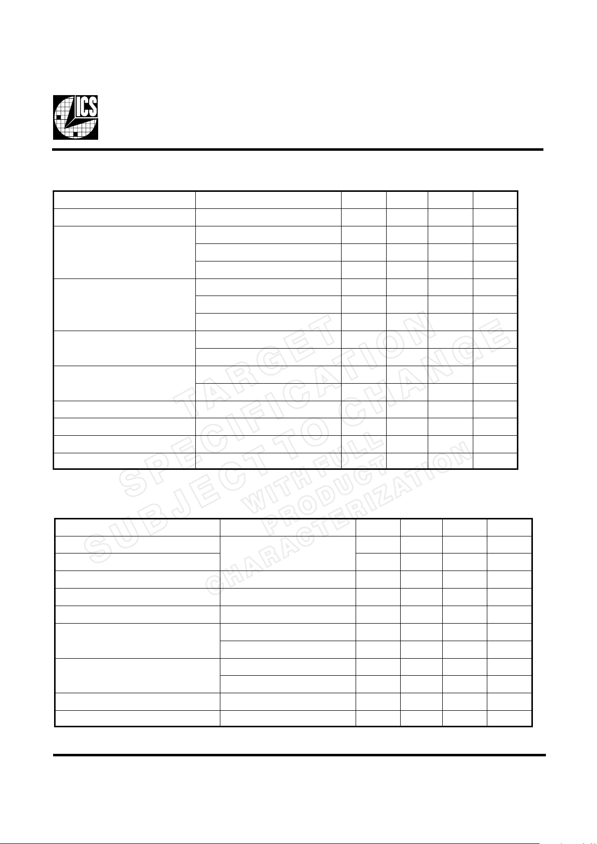
)detonesiwrehtosselnu(egnarerutarepmetria-eerfgnitarepodednemmocerrevoscitsiretcarahclacirtcelE
retemaraPsnoitidnoCtseTniMmoNxaMtinU
VegatlovtupnI
KI
V
DD
I,V3.3=
I
Am81=2.1-V
Vegatlovtuptuolevel-hgiH
HO
V
DD
I,xamotnim=
HO
Am1-=V
DD
2.0-V
V
DD
IV3=
HO
Am42=2 V
V
DD
IV3=
HO
Am21=4.2V
Vegatlovtuptuolevel-woL
LO
V
DD
I,xamotnim=
LO
Am1-=2.0V
V
DD
IV3=
LO
Am42=8.0V
V
DD
IV3=
LO
Am21=55.0V
Itnerructuptuolevel-hgiH
HO
V
DD
VV3=
O
V1=05-Am
V
DD
VV3.3=
O
V56.1=55-Am
Itnerructuptuolevel-woL
LO
V
DD
VV3=
O
V2=06Am
V
DD
VV3.3=
O
V56.1=07Am
ItnerructupnI
I
VIV=
O
Vro
DD
5±Aµ
I5erugifees,tnerruCcimanyD
DD
zHM76=f73Am
CecnaticapactupnI
i
V
DD
VV3.3=
I
VroV0=
DD
3Fp
CecnaticapactuptuO
o
V
DD
VV3.3=
I
VroV0=
DD
2.3Fp
,erutarepmetria-eerfgnitarepodnaegatlovylppusfosegnardednemmocerrevoscitsiretcarahcgnihctiwS
)2dna1serugifdna6etonees(V3.3=DDV,Fp52=LC
retemaraPsnoitidnoCtseTniMmoNxaMtinU
tyalednoitagaporpwol-ot-hgiH
HLP
2dna1serugifeeS
8.15.23sn
tyalednoitagaporphgih-ot-woL
LHP
8.14.23sn
T)4etonees(wekstuptuO
O(KS
)001sp
tweksesluP
)P(KS
V
HI
V=
DD
V,
LI
V0=051sp
TweksssecorP
)RP(KS
sn
T4erugifees,emithgihKLC
hgih
zHM666sn
zHM0413
T4erugifees,emitwolKLC
wol
zHM666sn
zHM0413
T‡etarwelsesirtuptuO
r
V2.0
DD
V6.0ot
DD
5.17.24 sn/V
T‡etarwelsllaftuptuO
f
V6.0
DD
V2.0ot
DD
5.17.24 sn/V
Page 4

4
ICS9112-27
Preliminary Product Preview
V
DD
0.6 V
DD
0.6 V
DD
50% V
DD
50% V
DD
50% V
DD
50% V
DD
0.2 V
DD
0.2 V
DD
V
OH
V
OL
CLK0-CLK3
Any CLK
Any CLK
50% V
DD
0V
t
PLH
t
R
t
f
T
sk(0)
T
PHL
CLKIN
CLK
n
V
DD
140W
10 pF
140W
Figure 1. Test Load Circuit
Figure 2. Voltage Thresholds for Propagation Delay (t ) Measurements
pd
Parameter Measurement Information
Figure 3. Output Skew
Figure 4. Clock Waveform
t
cyc
t
high
V
IH(Min)
V
test
V
IL(Max)
t
low
0.6 V
DD
0.2 V
DD
0.4 V
DD
Peak to Peak (Minimum)
Paramameter Value Unit
V
IH(Min)
0.5 V
DD
V
V
IL(Max)
0.35 V
DD
V
V
test
0.4 V
DD
V
Note: All parameters in Figure 4 are according to PCI-X 1.0 specifications.
Page 5

5
ICS9112-27
Preliminary Product Preview
High Level Output Voltage
vs
High-Level Output Current
I -High-Level Output Current-mA
Figure 6
OH
0
0.5
1.0
1.5
2.0
2.5
3.0
3.5
-100 -90 -80 -70 -60 -50 -40 -30 -20 -10 0
V - High-Level Output Voltage - V
OH
VDD = 3.3 V
TA = 25°C
Parameter Measurement Information
20
40
50
60
0 20 40 60 80 100 120 140 160
VDD = 3.6 V
TA = 85°C
Supply Current
vs
Frequency
F - Frequency - Mhz
Figure 5
I - Supply Current - mA
CC
Page 6

6
ICS9112-27
Preliminary Product Preview
VDD = 3.3 V
TA = 25°C
0
0.5
1.0
1.5
2.0
2.5
3.0
3.5
-20 0 20 40 60 80 100 120
Low Level Output Voltage
vs
Low-Level Output Current
I -Low-Level Output Current-mA
Figure 7
OL
Parameter Measurement Information
Page 7

7
ICS9112-27
Preliminary Product Preview
4.40 mm. Body, 0.65 mm. pitch TSSOP
(173 mil)
(0.0256 mil)
Ordering Information
ICS9112yG-27-T
Designation for tape and reel packaging
Pattern Number (2 or 3 digit number for parts with ROM code patterns)
Package Type
G=TSSOP
Revision Designator (will not correlate with datasheet revision)
Device Type (consists of 3 or 4 digit numbers)
Prefix
ICS, AV = Standard Device
Example:
ICS XXXX y G - PPP - T
MIN MAX MIN MAX
A - 1.20 - .047
A1 0.05 0.15 .002 .006
A2 0.80 1.05 .032 .041
b 0.19 0.30 .007 .012
c 0.09 0.20 .0035 .008
D
E
E1 4.30 4.50 .169 .177
e 0.65 BASIC 0.0256 BASIC
L 0.45 0.75 .018 .030
N
α
0° 8° 0° 8°
aaa - 0.10 - .004
VARIATIONS
MIN MAX MIN MAX
82.90
3.10
.114 .122
MO-153 JEDEC
Doc.# 10-0038
7/6/00 Rev B
N
D mm.
D (inch)
SEE VARIATIONS
SYMBOL
SEE VARIATIONS
SEE VARIATIONS
In Millimeters
COMMON DIMENSIONS
In Inches
COMMON DIMENSIONS
SEE VARIATIONS
6.40 BASIC 0.252 BASIC
PRODUCT PREVIEW documents contain information on new
products in the sampling or preproduction phase of development.
Characteristic data and other specifications are subject to change
without notice.
Page 8

8
ICS9112-27
Preliminary Product Preview
ICS XXXX y M - PPP - T
Ordering Information
ICS9112yM-27-T
Designation for tape and reel packaging
Pattern Number (2 or 3 digit number for parts with ROM code patterns)
Package Type
M=SOIC
Revision Designator (will not correlate with datasheet revision)
Device Type (consists of 3 or 4 digit numbers)
Prefix
ICS, AV = Standard Device
Example:
150 mil (Narrow Body) SOIC
MIN MAX MIN MAX
A 1.35 1.75 .0532 .0688
A1 0.10 0.25 .0040 .0098
B 0.33 0.51 .013 .020
C 0.19 0.25 .0075 .0098
D
E 3.80 4.00 .1497 .1574
e
H 5.80 6.20 .2284 .2440
h 0.25 0.50 .010 .020
L 0.40 1.27 .016 .050
N
α
0° 8° 0° 8°
VARIATIONS
MIN MAX MIN MAX
84.80
5.00
.1890 .1968
D mm.
D (inch)
SEE VARIATIONS
10-0030 Rev A - MS-012
SYMBOL
SEE VARIATIONS
SEE VARIATIONS
In Millimeters
COMMON DIMENSIONS
In Inches
COMMON DIMENSIONS
SEE VARIATIONS
1.27 BASIC 0.050 BASIC
N
PRODUCT PREVIEW documents contain information on new
products in the sampling or preproduction phase of development.
Characteristic data and other specifications are subject to change
without notice.
 Loading...